EP0121647A2 - PLA reprogrammable par des données dynamiques - Google Patents
PLA reprogrammable par des données dynamiques Download PDFInfo
- Publication number
- EP0121647A2 EP0121647A2 EP84100236A EP84100236A EP0121647A2 EP 0121647 A2 EP0121647 A2 EP 0121647A2 EP 84100236 A EP84100236 A EP 84100236A EP 84100236 A EP84100236 A EP 84100236A EP 0121647 A2 EP0121647 A2 EP 0121647A2
- Authority
- EP
- European Patent Office
- Prior art keywords
- coupled
- array
- input terminal
- control element
- multiplexor
- Prior art date
- Legal status (The legal status is an assumption and is not a legal conclusion. Google has not performed a legal analysis and makes no representation as to the accuracy of the status listed.)
- Granted
Links
Images

Classifications
-
- H—ELECTRICITY
- H03—ELECTRONIC CIRCUITRY
- H03K—PULSE TECHNIQUE
- H03K19/00—Logic circuits, i.e. having at least two inputs acting on one output; Inverting circuits
- H03K19/02—Logic circuits, i.e. having at least two inputs acting on one output; Inverting circuits using specified components
- H03K19/173—Logic circuits, i.e. having at least two inputs acting on one output; Inverting circuits using specified components using elementary logic circuits as components
- H03K19/177—Logic circuits, i.e. having at least two inputs acting on one output; Inverting circuits using specified components using elementary logic circuits as components arranged in matrix form
- H03K19/17704—Logic circuits, i.e. having at least two inputs acting on one output; Inverting circuits using specified components using elementary logic circuits as components arranged in matrix form the logic functions being realised by the interconnection of rows and columns
- H03K19/17708—Logic circuits, i.e. having at least two inputs acting on one output; Inverting circuits using specified components using elementary logic circuits as components arranged in matrix form the logic functions being realised by the interconnection of rows and columns using an AND matrix followed by an OR matrix, i.e. programmable logic arrays
- H03K19/17712—Logic circuits, i.e. having at least two inputs acting on one output; Inverting circuits using specified components using elementary logic circuits as components arranged in matrix form the logic functions being realised by the interconnection of rows and columns using an AND matrix followed by an OR matrix, i.e. programmable logic arrays one of the matrices at least being reprogrammable
Definitions
- This invention relates to programmable logic arrays (PLA's), and more particularly, to PLA's which are readily re-programmable.
- a PLA is a logic circuit which receives a plurality of digital input signals and generates a plurality of digital output signals wherein each of the digital output signals is a programmable sum-of-product combination of the input signals.
- one circuit is provided for generating a plurality of terms which are the logical AND of selected input signals; and another circuit is provided to generate the output signals by selectively ORing the AND terms.
- a typical PLA may have a total of n input signals, generate a total of m AND terms from the input signals, and generate a total of k output signals by selectively ORing the m AND terms.
- the general design of a PLA includes an AND array feeding into an OR array. These data lines feed an array of terms m deep. Each term is the AND combination of data, data complement and don't care for each input (don't care is formed by ignoring data and data complement for a given input), hence a typical program may appear as:
- PLA's are typically designed for use in systems requiring permanent or semipermanent nonvolatile logic arrays.
- PROM's programmable read only memories
- EPROM's erasable PROM's, can be changed by the use of an ultraviolet light, which erasure requires several hours to complete. Also, another problem with EPROM's is that they are expensive.
- An advantage of the present invention resides in the provision of a unique design that is readily adaptable to standard MOS (metal oxide semiconductor) fabrication techniques.
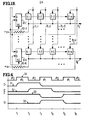
- An address line A l is coupled to first input terminals of each of the first-row elements 12-1, 12-2, 12-3...12-m.
- address line A 2 is coupled to first input terminals of the second-row elements 13-1, 13-2, 13-3...13-m; and, address line An is coupled to the nth row of program elements.
- the PLA program is loaded into the array by supplying serialized bits of the program on a "SERIAL IN" input terminal 15 while at the same time applying a high-level signal on a LOAD input terminal 16.
- the input terminal 15 is coupled to the first (A) input terminal of the multiplexor 14-1, and the input terminal 16 is coupled to the select (SEL) input terminals of the multiplexors 14-1, 14-2...14-n.
- All of the program elements of both the AND and the OR arrays are driven by the same clock.
- a high-level LOAD signal is applied on the terminal 16
- the A input terminal of each of the multiplexors is selected.
- a serial stream of data supplied on the SERIAL IN input terminal 15 will be shifted in a serpentine fashion through each of the rows of both the AND and the OR arrays.
- the multiplexor 18-1 is coupled to the first row of program elements 20-1, 20-2, 20-3...20-m of the OR array.
- a multiplexor 18-2 is coupled to the second row of elements 21-1, 21-2, 21-3...21-m; and, multiplexor 18-k is coupled to the last row of elements k-1, k-2, k-3...k-m.
- the select (SEL) input terminals of the multiplexors 18-1, 18-2...18-k are coupled to the LOAD input terminal 16. It should be noted that the program elements of the OR array are different from those of the AND array as will be described further hereinbelow.
- the second row elements are coupled to an output line 0 2 and the last row elements are coupled to an output line O k .
- the output lines O 1 , O 2 ...O k are biased at a high-level voltage (e.g., five volts) by means of resistors RO-1, RO-2...RO-k respectively, which are tied to a +V supply voltage.
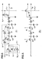
- the "CK" clock signal is supplied on a terminal 32, which is coupled to the input of an inverter 34 within the clock circuit 30.
- the output of the inverter 34 is the ⁇ 2 clock signal, and this output is coupled to the gate terminal of the transistor Q12 and to the input of an inverter 35.
- the output of the inverter 35 is the ⁇ 1 clock signal, and this output is coupled to the gate terminal of a transistor Q13.
- the ⁇ 1 and 0 2 clock signals are 180° out of phase (i.e., ⁇ 2 is the complement of 0 1 ).
- the drain terminal of the transistor Q12 is coupled to the input terminal of an inverter 36 at a node E and the output terminal of this inverter is coupled to the source terminal of Q13 at a node E.
- the drain terminal of Q13 is coupled to the input of an inverter 37 at a node F having an output terminal coupled to the gate terminal of a transistor Q14 and to the output of the element 12-1 on a line 38.
- a parasitic capacitance exists between the drain terminals of Q12 and Q13 and ground potential, which capacitors are referred to herein as C12 and C13.
- the line 38 is connected to the source terminal of a transistor within the next adjacent element 12-2 that corresponds to the source terminal of the transistor Q12.
- a high-level signal present at the circuit node D will be transferred to the circuit node E during the ⁇ 2 clock cycle. This signal level is retained by a charge on the capacitor C12. Simultaneously, the opposite logic level of E (i.e., E) will be present at the output of the inverter 36. During the ⁇ 1 clock cycle, the output of the inverter 36 (i.e., E) will be transferred to circuit node F whereupon it will appear inverted at the circuit node Q (line 38) as a result of the action of the inverter 37. The signal level at node F is retained by a charge on the capacitor C13.
- the address line A l is coupled to the gate terminal of a transistor Q15 having a source terminal coupled to the term line TL-1.
- the drain terminal of Q15 is coupled to the source terminal of Q14 and the drain terminal of Q14 is coupled to ground potential.
- FIG. 3 Before describing the operation of the circuit shown in FIG. 2, reference is briefly made to FIG. 3 wherein the program element 20-1 of the OR array is shown for comparison purposes. Like reference numerals are used in FIG. 3 with the addition of a prime.
- the major difference between an AND array element and an OR array element is the manner in which Q15 9 is connected. Note in FIG. 2 that the gate to Ql5 is controlled by an address line (e.g., A l ) and the source terminal is coupled to the term line TL-1.
- the gate terminal of Q15' is coupled to the term line and the drain terminal is coupled to an output line (e.g., 0 1 ).
- Waveform 50 represents the ⁇ 1 clock signal and the ⁇ 2 clock signal is the complement of ⁇ 1 , as noted in the drawing.
- Waveform 51 illustrates a data bit (high-level signal) appearing at the input of the program element 12-1 (node D) by means of either Q10 or Qll (input A or B, respectively) of the multiplexor 14-1.
- Waveform 52 illustrates the signal at the input of the inverter 36 (node E), and waveform 53 represents the signal at the input of the inverter 37 (node F).
- Waveform 54 represents the inverse of waveform 53 as inverted by the inverter 37 (node Q).
- the high-level signal at the output of the inverter 37 (node Q), as represented by the waveform 54 between times t 3 and t 5 will turn on the transistor Q14. If a high-level signal is present on the address line A 1 at the same time, the term line TL-1 will be pulled down to ground potential. In a similar manner, a high-level signal at the output of the inverter 37 1 (FIG. 3) will turn on the transistor Q14'. If the term line TL-1 has not been pulled down to ground potential as in the previous example, Q15' will turn on (remember that the term line TL-1 is biased to +V through resistor R-1), which will cause the output line O 1 to drop to ground potential. On the other hand, if as in the previous example the term line TL-1 has been pulled down to ground potential, 015' will be turned off and the state of the line 38 1 would be irrelevant.
- the LOAD signal is removed (i.e., drops to a low level) from the terminal 16.
- the transistor Q10 is turned off and the transistor Qll is turned on. This occurs at the same time in all of the multiplexors 14-1, 14-2...14-n, 18-1, 18-2...18-k.
- the clock (CK) signals are continuously supplied to the program elements so that the program will circulate within each row. That is, the data stored in the element 12-1 will be shifted to the element 12-2, etc., and the data stored in the element 12-m will be shifted back to the element 12-1. It is this continuous circulation of the programmed data in each row that obviates refresh logic.
- a static program element is larger in area (requires more silicon real estate) than are dynamic program elements.
- the data stored in a dynamic program element will decay with time and must be refreshed periodically.
- One approach for refreshing the program element is to use refresh logic as is typically employed in dynamic RAM's.
- Another approach that requires even less real estate is to continuously shift the data through amplifiers as is disclosed and claimed in this application.
- the inverters 36 and 37 are also amplifiers that amplify the charge present on either capacitor C12 or C13. Stated otherwise, the charge on the capacitors will decay over time. However, the frequency of the clock is typically set sufficiently fast so as to restore the charge prior to it decaying below the threshold level of the inverters. Since the discharge time is approximately two milliseconds, the minimum clock frequency is 500 hertz. In one embodiment, however, the clock is set at a substantially higher frequency within the range of approximately one to four megahertz.
Landscapes
- Physics & Mathematics (AREA)
- Mathematical Physics (AREA)
- Engineering & Computer Science (AREA)
- Computer Hardware Design (AREA)
- Computing Systems (AREA)
- General Engineering & Computer Science (AREA)
- Logic Circuits (AREA)
Applications Claiming Priority (2)
| Application Number | Priority Date | Filing Date | Title |
|---|---|---|---|
| US06/457,177 US4524430A (en) | 1983-01-11 | 1983-01-11 | Dynamic data re-programmable PLA |
| US457177 | 1983-01-11 |
Publications (3)
| Publication Number | Publication Date |
|---|---|
| EP0121647A2 true EP0121647A2 (fr) | 1984-10-17 |
| EP0121647A3 EP0121647A3 (en) | 1986-05-07 |
| EP0121647B1 EP0121647B1 (fr) | 1989-05-31 |
Family
ID=23815742
Family Applications (1)
| Application Number | Title | Priority Date | Filing Date |
|---|---|---|---|
| EP84100236A Expired EP0121647B1 (fr) | 1983-01-11 | 1984-01-11 | PLA reprogrammable par des données dynamiques |
Country Status (4)
| Country | Link |
|---|---|
| US (1) | US4524430A (fr) |
| EP (1) | EP0121647B1 (fr) |
| JP (2) | JPS59161130A (fr) |
| DE (1) | DE3478551D1 (fr) |
Cited By (4)
| Publication number | Priority date | Publication date | Assignee | Title |
|---|---|---|---|---|
| GB2184878A (en) * | 1985-02-14 | 1987-07-01 | Intel Corp | Software programmable logic array |
| GB2212958A (en) * | 1985-02-14 | 1989-08-02 | Intel Corp | Software programmable logic array |
| EP0585119A1 (fr) * | 1992-08-27 | 1994-03-02 | AT&T GLOBAL INFORMATION SOLUTIONS INTERNATIONAL INC. | Dispositif logique programmable |
| US5594698A (en) * | 1993-03-17 | 1997-01-14 | Zycad Corporation | Random access memory (RAM) based configurable arrays |
Families Citing this family (14)
| Publication number | Priority date | Publication date | Assignee | Title |
|---|---|---|---|---|
| JPH0638318B2 (ja) * | 1985-02-15 | 1994-05-18 | 株式会社リコー | Epromの書込み方法 |
| US4791603A (en) * | 1986-07-18 | 1988-12-13 | Honeywell Inc. | Dynamically reconfigurable array logic |
| US4730130A (en) * | 1987-01-05 | 1988-03-08 | Motorola, Inc. | Writable array logic |
| JPH0611113B2 (ja) * | 1988-01-14 | 1994-02-09 | 川崎製鉄株式会社 | プログラマブル論理素子 |
| US4930107A (en) * | 1988-08-08 | 1990-05-29 | Altera Corporation | Method and apparatus for programming and verifying programmable elements in programmable devices |
| US5132570A (en) * | 1988-08-31 | 1992-07-21 | Fujitsu Limited | Extended logical scale structure of a programmable logic array |
| US5023838A (en) * | 1988-12-02 | 1991-06-11 | Ncr Corporation | Random access memory device with integral logic capability |
| US4940909A (en) * | 1989-05-12 | 1990-07-10 | Plus Logic, Inc. | Configuration control circuit for programmable logic devices |
| US5099150A (en) * | 1989-09-29 | 1992-03-24 | Sgs-Thomson Microelectronics, Inc. | Circuit block for programmable logic devices, configurable as a user-writable memory or a logic circuit |
| US4975601A (en) * | 1989-09-29 | 1990-12-04 | Sgs-Thomson Microelectronics, Inc. | User-writable random access memory logic block for programmable logic devices |
| US5128559A (en) * | 1989-09-29 | 1992-07-07 | Sgs-Thomson Microelectronics, Inc. | Logic block for programmable logic devices |
| US5084636A (en) * | 1989-12-27 | 1992-01-28 | Kawasaki Steel | Master-slave programmable logic devices |
| US5555214A (en) * | 1995-11-08 | 1996-09-10 | Altera Corporation | Apparatus for serial reading and writing of random access memory arrays |
| US7183801B2 (en) * | 2004-09-08 | 2007-02-27 | Atmel Corporation | Programmable logic auto write-back |
Family Cites Families (4)
| Publication number | Priority date | Publication date | Assignee | Title |
|---|---|---|---|---|
| JPS525742A (en) * | 1975-07-01 | 1977-01-17 | Toray Eng Co Ltd | Process for dechlorination of pcb |
| DE3015992A1 (de) * | 1980-04-25 | 1981-11-05 | Ibm Deutschland Gmbh, 7000 Stuttgart | Programmierbare logische anordnung |
| JPS57117168A (en) * | 1981-01-08 | 1982-07-21 | Nec Corp | Memory circuit |
| JPS57129537A (en) * | 1981-02-05 | 1982-08-11 | Toshiba Corp | Programmable array circuit |
-
1983
- 1983-01-11 US US06/457,177 patent/US4524430A/en not_active Expired - Lifetime
-
1984
- 1984-01-10 JP JP59003346A patent/JPS59161130A/ja active Pending
- 1984-01-11 DE DE8484100236T patent/DE3478551D1/de not_active Expired
- 1984-01-11 EP EP84100236A patent/EP0121647B1/fr not_active Expired
-
1990
- 1990-10-23 JP JP2286919A patent/JPH03187521A/ja active Granted
Cited By (8)
| Publication number | Priority date | Publication date | Assignee | Title |
|---|---|---|---|---|
| GB2184878A (en) * | 1985-02-14 | 1987-07-01 | Intel Corp | Software programmable logic array |
| GB2212958A (en) * | 1985-02-14 | 1989-08-02 | Intel Corp | Software programmable logic array |
| GB2184878B (en) * | 1985-02-14 | 1989-11-01 | Intel Corp | Software programmable logic array |
| GB2171231B (en) * | 1985-02-14 | 1989-11-01 | Intel Corp | Software programmable logic array |
| GB2212958B (en) * | 1985-02-14 | 1989-11-22 | Intel Corp | Software programmable logic array |
| EP0585119A1 (fr) * | 1992-08-27 | 1994-03-02 | AT&T GLOBAL INFORMATION SOLUTIONS INTERNATIONAL INC. | Dispositif logique programmable |
| US5432388A (en) * | 1992-08-27 | 1995-07-11 | At&T Global Information Solutions Company | Repeatedly programmable logic array using dynamic access memory |
| US5594698A (en) * | 1993-03-17 | 1997-01-14 | Zycad Corporation | Random access memory (RAM) based configurable arrays |
Also Published As
| Publication number | Publication date |
|---|---|
| US4524430A (en) | 1985-06-18 |
| EP0121647A3 (en) | 1986-05-07 |
| JPH03187521A (ja) | 1991-08-15 |
| JPS59161130A (ja) | 1984-09-11 |
| EP0121647B1 (fr) | 1989-05-31 |
| DE3478551D1 (de) | 1989-07-06 |
| JPH057899B2 (fr) | 1993-01-29 |
Similar Documents
| Publication | Publication Date | Title |
|---|---|---|
| US4524430A (en) | Dynamic data re-programmable PLA | |
| US4546273A (en) | Dynamic re-programmable PLA | |
| US4037089A (en) | Integrated programmable logic array | |
| US4706216A (en) | Configurable logic element | |
| EP0122363B1 (fr) | PLA reprogrammable | |
| US4445204A (en) | Memory device | |
| JPH0369095A (ja) | 2導体のデータカラムを有する記憶論理アレイに使用する記憶セル | |
| CA2154802A1 (fr) | Memoire a circuit integre | |
| EP0137135A2 (fr) | Mémoire semi-conductrice | |
| US3851313A (en) | Memory cell for sequentially addressed memory array | |
| US3609391A (en) | Timing pulse generator | |
| EP0383387B1 (fr) | Circuit intégré | |
| US3644907A (en) | Complementary mosfet memory cell | |
| EP0244142A2 (fr) | Registre de données en technologie CMOS | |
| US4691302A (en) | Circuit arrangement comprising a matrix-shaped memory arrangement for variably adjustable delay of digital signals | |
| EP0115140B1 (fr) | Circuit décodeur | |
| US5692164A (en) | Method and apparatus for generating four phase non-over lapping clock pulses for a charge pump | |
| US3636376A (en) | Logic network with a low-power shift register | |
| EP0051157B1 (fr) | Cellule exécutant une combinaison logique pour utilisation dans des structures du type PLA | |
| US4984215A (en) | Semiconductor memory device | |
| EP0138406A2 (fr) | Registre à décalage | |
| US4757218A (en) | Semiconductor IC device with word lines shielded from voltage changes in adjacent lines | |
| EP0144635B1 (fr) | Agencement de circuits logiques | |
| KR950004742B1 (ko) | 반도체 메모리용 시리얼 선택회로 및 그 작동방법 | |
| US3704454A (en) | Accessing system for and in integrated circuit type memories |
Legal Events
| Date | Code | Title | Description |
|---|---|---|---|
| PUAI | Public reference made under article 153(3) epc to a published international application that has entered the european phase |
Free format text: ORIGINAL CODE: 0009012 |
|
| AK | Designated contracting states |
Designated state(s): BE DE FR GB NL SE |
|
| PUAL | Search report despatched |
Free format text: ORIGINAL CODE: 0009013 |
|
| AK | Designated contracting states |
Kind code of ref document: A3 Designated state(s): BE DE FR GB NL SE |
|
| 17P | Request for examination filed |
Effective date: 19860909 |
|
| RAP1 | Party data changed (applicant data changed or rights of an application transferred) |
Owner name: BURROUGHS CORPORATION (A DELAWARE CORPORATION) |
|
| 17Q | First examination report despatched |
Effective date: 19870924 |
|
| GRAA | (expected) grant |
Free format text: ORIGINAL CODE: 0009210 |
|
| RAP1 | Party data changed (applicant data changed or rights of an application transferred) |
Owner name: UNISYS CORPORATION (A DELAWARE CORP.) |
|
| AK | Designated contracting states |
Kind code of ref document: B1 Designated state(s): BE DE FR GB NL SE |
|
| RAP2 | Party data changed (patent owner data changed or rights of a patent transferred) |
Owner name: UNISYS CORPORATION |
|
| REF | Corresponds to: |
Ref document number: 3478551 Country of ref document: DE Date of ref document: 19890706 |
|
| ET | Fr: translation filed | ||
| BECN | Be: change of holder's name |
Effective date: 19890531 |
|
| PLBE | No opposition filed within time limit |
Free format text: ORIGINAL CODE: 0009261 |
|
| STAA | Information on the status of an ep patent application or granted ep patent |
Free format text: STATUS: NO OPPOSITION FILED WITHIN TIME LIMIT |
|
| 26N | No opposition filed | ||
| PGFP | Annual fee paid to national office [announced via postgrant information from national office to epo] |
Ref country code: DE Payment date: 19910130 Year of fee payment: 8 |
|
| REG | Reference to a national code |
Ref country code: GB Ref legal event code: 732 |
|
| REG | Reference to a national code |
Ref country code: FR Ref legal event code: TP |
|
| NLS | Nl: assignments of ep-patents |
Owner name: HYUNDAI ELECTRONICS INDUSTRIES LTD. TE SEOUL, ZUID |
|
| PG25 | Lapsed in a contracting state [announced via postgrant information from national office to epo] |
Ref country code: DE Effective date: 19921001 |
|
| EAL | Se: european patent in force in sweden |
Ref document number: 84100236.3 |
|
| PGFP | Annual fee paid to national office [announced via postgrant information from national office to epo] |
Ref country code: GB Payment date: 20000105 Year of fee payment: 17 |
|
| PGFP | Annual fee paid to national office [announced via postgrant information from national office to epo] |
Ref country code: SE Payment date: 20000107 Year of fee payment: 17 |
|
| PGFP | Annual fee paid to national office [announced via postgrant information from national office to epo] |
Ref country code: FR Payment date: 20000112 Year of fee payment: 17 |
|
| PGFP | Annual fee paid to national office [announced via postgrant information from national office to epo] |
Ref country code: NL Payment date: 20000131 Year of fee payment: 17 |
|
| PGFP | Annual fee paid to national office [announced via postgrant information from national office to epo] |
Ref country code: BE Payment date: 20000315 Year of fee payment: 17 |
|
| PG25 | Lapsed in a contracting state [announced via postgrant information from national office to epo] |
Ref country code: GB Free format text: LAPSE BECAUSE OF NON-PAYMENT OF DUE FEES Effective date: 20010111 |
|
| PG25 | Lapsed in a contracting state [announced via postgrant information from national office to epo] |
Ref country code: SE Free format text: LAPSE BECAUSE OF NON-PAYMENT OF DUE FEES Effective date: 20010112 |
|
| PG25 | Lapsed in a contracting state [announced via postgrant information from national office to epo] |
Ref country code: BE Free format text: LAPSE BECAUSE OF NON-PAYMENT OF DUE FEES Effective date: 20010131 |
|
| BERE | Be: lapsed |
Owner name: HYUNDAI ELECTRONICS INDUSTIRES LTD Effective date: 20010131 |
|
| PG25 | Lapsed in a contracting state [announced via postgrant information from national office to epo] |
Ref country code: NL Free format text: LAPSE BECAUSE OF NON-PAYMENT OF DUE FEES Effective date: 20010801 |
|
| GBPC | Gb: european patent ceased through non-payment of renewal fee |
Effective date: 20010111 |
|
| EUG | Se: european patent has lapsed |
Ref document number: 84100236.3 |
|
| PG25 | Lapsed in a contracting state [announced via postgrant information from national office to epo] |
Ref country code: FR Free format text: LAPSE BECAUSE OF NON-PAYMENT OF DUE FEES Effective date: 20010928 |
|
| NLV4 | Nl: lapsed or anulled due to non-payment of the annual fee |
Effective date: 20010801 |
|
| REG | Reference to a national code |
Ref country code: FR Ref legal event code: ST |