EP0124265A2 - Bilderzeugungsverfahren mit negativen Schutzschichten - Google Patents
Bilderzeugungsverfahren mit negativen Schutzschichten Download PDFInfo
- Publication number
- EP0124265A2 EP0124265A2 EP84302145A EP84302145A EP0124265A2 EP 0124265 A2 EP0124265 A2 EP 0124265A2 EP 84302145 A EP84302145 A EP 84302145A EP 84302145 A EP84302145 A EP 84302145A EP 0124265 A2 EP0124265 A2 EP 0124265A2
- Authority
- EP
- European Patent Office
- Prior art keywords
- resist
- patterns
- ultraviolet rays
- film
- substrate
- Prior art date
- Legal status (The legal status is an assumption and is not a legal conclusion. Google has not performed a legal analysis and makes no representation as to the accuracy of the status listed.)
- Granted
Links
Images
Classifications
-
- G—PHYSICS
- G03—PHOTOGRAPHY; CINEMATOGRAPHY; ANALOGOUS TECHNIQUES USING WAVES OTHER THAN OPTICAL WAVES; ELECTROGRAPHY; HOLOGRAPHY
- G03F—PHOTOMECHANICAL PRODUCTION OF TEXTURED OR PATTERNED SURFACES, e.g. FOR PRINTING, FOR PROCESSING OF SEMICONDUCTOR DEVICES; MATERIALS THEREFOR; ORIGINALS THEREFOR; APPARATUS SPECIALLY ADAPTED THEREFOR
- G03F7/00—Photomechanical, e.g. photolithographic, production of textured or patterned surfaces, e.g. printing surfaces; Materials therefor, e.g. comprising photoresists; Apparatus specially adapted therefor
- G03F7/004—Photosensitive materials
- G03F7/022—Quinonediazides
Definitions
- This invention relates to a process for forming fine patterns with a negative resist suitable for fabrication of semiconductors, magnetic bubble elements, light applied components and the like.
- the lithographic technique wherein such far ultraviolet rays as mentioned above are utilized is not only an extension technique of conventional photolithography, but also a technique wherein submicron transfer becomes easily possible.
- such lithographic technique may be much expected for future fine workings. These fine workings may be classified into an etching method and a lift-off method.
- the aforesaid objects of the present invention are attained by the steps of exposing a resist film by means of far ultraviolet rays, developing the resist film thus exposed to form resist patterns, and thereafter subjecting the whole surface of a substrate involving the aforesaid resist patterns to blanket irradiation with ultraviolet rays prior to application of a layer to be patterned.
- naphthoquinone-1,2-diazide-5-sulfonic ester (hereinafter referred to simply as "LMR") of novolak resin having a polymerization degree of 10 or less is suitably used as a resist material as described in the under-mentioned examples.
- LMR naphthoquinone-1,2-diazide-5-sulfonic ester
- benzoquinone diazide, naphthoquinone diazide and the like are known as quinone diazide groups and any of them may be employed in the present invention to obtain the same effects with each other.
- the aforesaid LMR has 10 times or higher sensitivity than that of PMMA with respect to far ultraviolet rays so that submicron transfer is possible, and the resist patterns obtained therefrom are excellent in dry etching resistance. Further, no sags are observed on such patterns even at a baking temperature of about 200°C. In addition, overhung form in patterns can be obtained by the use of the resist material of LMR with only developing treatment.
- the aforesaid LMR may suitably be utilized as both a resist for dry etching and a resist for lift-off method in accordance with far ultraviolet lithography.
- Mechanism for favorably forming negative resist patterns by means of far ultraviolet rays according to the present invention as described above may be considered as follows.
- reaction due to far ultraviolet rays quite differs from the reaction by means of ordinary ultraviolet irradiation.
- the resist of a part irradiated with far ultraviolet rays in the present invention is subjected to structural change so that such part becomes insoluble in acetic ester or the like to obtain patterns. More specifically, although the resist is a negative resist, formation of patterns thereof is not conducted in accordance with crosslinking reaction so that there is no swelling of patterns and as a result, the resultant patterns exhibit significantly high resolving power.
- LMR is a kind of oligomer, and low molecular weight thereof will also contribute to such high resolving power of the patterns.
- LMR is a compound in which quinone diazide is combined with novolak by means of sulfonic acid, and it may be considered from, for example, Comparative Example 4 that the structural change is not effected by reaction of novolak, but is effected by that of quinone diazide group with the irradiation of far ultraviolet rays.
- the polymer which can be utilized in the present invention is required to involve quinone diazide group, and further to be soluble in acetic ester, alkyl ketone, cyclohexanone or the like.
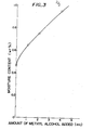
- Example 12 For instance, a developer described in the under- mentioned Example 12 exhibits low solubility of water so that saturation content of water is 0.46% in the developer. Such content of water will be described in more detail hereinbelow.
- Figure 3 is a graphic representation indicating characteristic curve wherein moisture content in a developer is plotted as ordinate in wt% with respect to amount (ml) of methyl alcohol added plotted as abscissa in the case where 2 ml of water is added to 100 ml of the developer consisting of 10 isoamyl acetate and 2 cyclohexane in volume ratio, and methyl alcohol is further added to the resultant mixture.
- methanol when methanol is added to the developer, moisture content in the developer increases. More specifically, when 4 ml of methanol is added to 100 ml of the developer, moisture content reaches 0.97% by weight.
- Such high sensitivity of the resist patterns due to heating is supposed to be based on such fact that the reaction does not proceed up to obtaining 100% final product (insoluble in isoamyl acetate) by only irradiation with far ultraviolet rays, but the product remains in a state of an intermediate (insoluble in amyl acetate), and such intermediate does not shift to the final product until the former is heated.
- the lower limit of temperature conditions for such heating as described above is about 50°C, whilst patterns cannot be obtained at, for example, 130°C exceeding the upper limit. This is because there arises thermal crosslinking due to decomposition of quinone diazide group at a temperature of 130°C or more in the LMR so that such LMR becomes insoluble in the solvent.
- the heating after exposure is carried out at a temperature of 50 - 120°C as described above, and particularly 80 - 110°C is preferable.
- the exposure is conducted in such a manner that first, a resist film is subjected to blanket exposure by means of ultraviolet rays having a longer wavelength than 300 nm and then, the resist film thus blanket-exposed to ultraviolet rays is subjected to selective exposure again by means of far ultraviolet rays of 300 nm or less with the utilization of a mask for forming patterns, and thereafter the resist film thus exposed twice is developed.
- Amount of exposure by far ultraviolet rays in the present invention is about three times or higher than that where no ultraviolet irradiation is carried out, but the throughput and the like are not substantially affected adversely by such an extent of exposure amount.
- the object of the present invention is further attained by subjecting a region to be left as the above-mentioned resist patterns to selective exposure with far ultraviolet rays at a wavelength of 200 - 300 nm, whilst subjecting a region to be removed to exposure by means of ultraviolet rays having a wavelength longer than 300 nm.
- the process for forming patterns according to the present invention utilizes such phenomena that the resist is made to be insoluble (negative) in the developer by means of selective irradiation with far ultraviolet rays, rate of dissolution of the resist is accelerated by means of ultraviolet irradiation, light absorption of the resist is noticeable in wavelength region of far ultraviolet rays so that light permeates only such an area extending immediately under the surface layer of the resist, and light reaches the surface of the substrate in wavelength region of ultraviolet rays, even if the resist film is thick. Therefore it is apparent that the process according to the present invention may be applied to any resist material which exhibits such phenomena as enumerated above, and the same excellent advantages with those mentioned above can also be attained by such pertinent resist materials.
- LMR was dissolved in methyl cellosolve acetate, and the resulting solution was applied to a silicon substrate with a thickness of 0.5 ⁇ m in accordance with spin coating method.
- the substrate thus applied was baked at 60°C for 30 minutes, and subjected to contact exposure for 10 seconds by means of 500 W Xe-Hg lamp. After the exposure, the so-treated substrate was developed for 20 seconds by using isoamyl acetate to obtain negative resist patterns of 0.5 ⁇ m line-and-space.
- Example 1 The resist patterns obtained in Example 1 were heated at 200°C for 30 minutes, and observed by means of SEM. As a result, no deformation such as sags or the like was observed on the resist patterns which were equivalent to those prior to the heating.
- a film was formed on a substrate from LMR in accordance with the same manner as that of Example 1, and dry etching resistance thereof was examined in case of using oxygen plasma wherein a parallel plate type etching device was used to carry out etching for 15 minutes at 0.08 W/cm 2 output density, 20 SccM 0 2 gas flow rate, and 50 pa gas pressure. As a result, etching amount was 50 nm, and for the comparison, another etching was carried out under the same conditions except that PMMA was employed, the etching amount of which was 200 nm.
- Example 2 LMR was exposed in accordance with the same manner as that of Example 1, and developed by utilizing AZ-1350J exclusive developer for 60 seconds. As a result, no patterns were formed.
- PMMA was applied on a silicon substrate with a thickness of 0.5 ⁇ m, and prebaked at 180°C for 30 minutes. Thereafter the substrate thus prebaked was exposed by utilizing the same device as that of Example 1 for 60 seconds and 120 seconds, respectively, and the substrates thus exposed were developed by the use of MIBK. As a result, patterns were obtained in case of 120 seconds exposure, whilst no patterns were obtained in 60 seconds exposure.
- Example 2 LMR formed by the same manner as that of Example 1 was exposed by utilizing a mask aligner provided with 250 W mercury-arc lamp for 30 seconds, and developed by means of AZ-1350J developer to obtain positive type patterns. On the other hand, as a result of the development by the use of isoamyl acetate, the whole surface of the film was dissolved therein to obtain no patterns.
- Novolak resin was dissolved in methyl cellosolve acetate, the resulting solution was applied to a substrate with a thickness of 0.5 ⁇ m, and prebaked at 100°C for 30 minutes. Exposure was carried out in accordance with the same manner as that of Example 1, and thereafter the so-treated substrate was developed by the use of isoamyl acetate. However, no patterns were formed on the substrate.
- LMR was dissolved in methyl cellosolve acetate, the resulting solution was filtered with a filter of 0.2 ⁇ m, and then applied on a silicon substrate with a thickness of 0.6 ⁇ m to form a film, i.e., resist film. Thereafter the substrate provided with the resist film was subjected to heat-treatment (prebaking) at a temperature of 60°C for 30 minutes, and then the resulting resist film was exposed by means of principally far ultraviolet rays of 180 - 300 nm derived from 500 W Xe-Hg lamp through a mask contacted closely to the resist film for 5, 8 and 10 seconds, respectively.
- prebaking heat-treatment
- Example 8 exposure was conducted in the same manner as that of Example 8 except that a thickness of LMR resist film was 1.2 ⁇ m and an exposure time was 10 seconds. After the exposure, the substrate with the resist film was heated at 100°C for 30 minutes, and then developed with a mixed solution prepared by adding 0.002 water to 1:1 admixture of cyclohexanone and cyclohexane in volume ratio for 15 seconds to form patterns. As a result, 0.5 ⁇ m space patterns were obtained. In addition, it was confirmed that no cracks were produced in the resist film with the resulting resist patterns.
- a resist film was formed, heated and exposed in accordance with the same manner as that of Example 8, then heated at 100°C for 30 minutes, and thereafter developed with a mixed solution prepared by adding 4 isopropyl alcohol to 2 cyclohexanone for 20 seconds to form patterns. As a result, 0.5 ⁇ m line-and-space resist patterns were obtained.
- the developing temperature was 23°C.
- LMR having a polymerization degree of 10 or less was dissolved in methyl cellosolve acetate, and the resulting solution was applied on a silicon substrate in accordance with spin coating method to form a resist film having a thickness of 2 ⁇ m. Then, the substrate provided with the resist film was subjected to heat treatment (prebaking) in nitrogen atmosphere at a temperature of 60°C for 30 minutes, and thereafter exposed by means of principally far ultraviolet rays of 180 - 300 nm derived from 500 W Xe-Hg lamp for 10 seconds in accordance with contact method in which a mask is closely contacted with the resist film.
- prebaking heat treatment
- the resulting sample was then subjected to heat treatment in nitrogen atmosphere at a temperature of 100°C for 30 minutes, and thereafter the resist film was developed by the use of a well agitated solution which had been obtained by adding 2 ml of water and 2 ml of methyl alcohol to 100 ml of a developer (mixed solvent) prepared by adding 2 cyclohexane to 10 isoamyl acetate in volume ratio.
- a temperature of the solution was 23°C and a period of development was 15 seconds.
- a resist film was exposed in the same manner as that of Example 12, and then heated in nitrogen atmosphere at a temperature of 100°C for 30 minutes. Then a solution obtained by adding 2 ml of water and 3 ml of methyl alcohol to 100 ml of a developer prepared by adding 3 cyclohexane to 2 cyclohexanone in volume ratio (in this case, a temperature of the solution being 23°C) was well agitated, and the resist film heated as described above was developed with the aforesaid solution to form patterns. As a result, 0.5 space patterns were obtained. Further it was confirmed that a profile of the resist film provided with the resulting resist patterns exhibited an overhung form, and no cracks were observed in the resist film. In this case also, the resist film had more favorable thermal resistance, solubility, and adhesive properties than those of a conventional resist film.
- Such a resist film obtained by conducting exposure in accordance with the same manner as that of Example 12 and then being subjected to heat-treatment in nitrogen atmosphere at a temperature of 100°C for 30 minutes was utilized as a sample.
- a solution was obtained by adding 2 ml of water only to 100 ml of a developer prepared by adding 2 cyclohexane to 10 isoamyl acetate in volume ratio (in this case also, a temperature of the solution being 23°C), the resulting solution was sufficiently stirred, and the aforesaid sample was developed by means of this solution.
- 0.75 ⁇ m patterns were obtained. In this case, however, it was confirmed that some cracks were produced on peripheral portions of the patterns.
- LMR was dissolved in methyl cellosolve acetate, filtered with 0.2 ⁇ m filter, and applied on a Si substrate with a thickness of 0.6 ⁇ m.
- the substrate with the resulting film was baked at 60°C for 30 minutes, and exposed by means of 500 W Xe-Hg lamp in accordance with contact method for 3, 5 and 10 seconds, respectively.
- Example 14 The same exposure was carried out as in Example 14, and immediately after the exposure, development was conducted by means of the same developer as that of Example 14. As a result, patterns could be formed in case of 10 second exposure while no patterns could be obtained in cases of 3 second and 5 second exposures.
- Example 14 The same exposure was carried out as in Example 14, the samples were heated at 50°C and 130°C for 30 minutes, and the same development was conducted in accordance with the same manner as that of Example 14.
- the sample in case of 50°C heating could be resolved at 5 second and 10 second exposures whilst resolution was insufficient at 3 second exposure.
- all the patterns did not dissolve in the developer so that no patterns could be obtained.
- LMR was dissolved in methyl cellosolve acetate, and the resulting solution was applied on a silicon substrate with a thickness of 1 ⁇ m to form a resist film.
- the substrate provided with the resist film was subjected to heat treatment (prebaking) at a temperature of 60°C for 30 minutes, and thereafter an initial exposing step was conducted.
- the resulting resist film was subjected to blanket irradiation with ultraviolet rays of only more than 300 nm, preferably 350 - 450 nm which were obtained by cutting out the light having wavelengthes of 300 nm and shorter ones in the light derived from 250 W Hg lamp for 60 seconds.
- the resist film exposed initially was subjected to selective exposure in such a manner that only the portions to be left as resist patterns were irradiated with far ultraviolet rays of 200 - 300 nm from 500 W Xe-Hg lamp through a mask according to contact method for 30 seconds.
- the resulting resist film was developed by means of a solution prepared by saturating a mixture of 10 isoamyl acetate and 5 cyclohexane in volume ratio with water for 30 seconds, and in this case, a temperature of the development was 23°C.
- a layer to be applied e.g., an Al layer was evaporated with a thickness of 1 pm on the substrate on which the resist patterns had been formed in accordance with vacuum deposition method.
- an organic solvent e.g., acetone solution
- lift-off was completely performed and 0.5 ⁇ m line-and-space Al patterns could be obtained.
- LMR was dissolved in methyl cellosolve acetate, and the resulting solution was applied on a silicon substrate with a thickness of 2 pm to form a resist film. Then, the substrate with the resist film was heat-treated (prebaked) at a temperature of 60°C for 30 minutes, and thereafter the resist film thus heat-treated was selectively exposed through a mask by means of far ultraviolet rays of 200 - 300 nm derived from 500 W Xe-Hg lamp for 5 seconds thereby to form a region irradiated with far ultraviolet rays.
- a reverse mask to the former was applied, through which selective exposure was conducted by the use of ultraviolet rays having a longer wavelength than 300 nm derived from an extra-high pressure Hg lamp for 60 seconds thereby to form a region irradiated with ultraviolet rays.
- solubility in the region irradiated with ultraviolet rays was improved with respect to a developer used, and such irradiation effect with ultraviolet rays appeared after the irradiation for several seconds and reached saturation for about 60 seconds.
- the resulting sample was heat-treated at a temperature of 100°C for 30 minutes, and thereafter the resist film thus heat-treated was developed by utilizing a solution prepared by saturating a mixture of 10 isoamyl acetate and 5 cyclohexane in volume ratio with water at a temperature of the solution of 23°C for 60 seconds.
- Al was evaporated with a thickness of 1.5 ⁇ m on the surface of the substrate involving such resist patterns as mentioned above in accordance with vacuum deposition method.
- the resulting sample was then immersed in an organic solvent, e.g., acetone solution to effect lift-off.
- an organic solvent e.g., acetone solution
- Example 17 The same resist film as that of Example 17 was selectively exposed through a mask by means of far ultraviolet rays of 200 - 300 nm derived from 500 W Xe-Hg lamp for 5 seconds without accompanying irradiation with ultraviolet rays derived from such an extra-high pressure Hg lamp as in Example 17. Then followed by heat treatment of the resulting sample at a temperature of 100°C for 30 minutes, thereafter development was conducted by using a solution prepared by saturating a mixture of 10 isoamyl acetate and 2 cyclohexane in volume ratio with water.
- LMR was dissolved in methyl cellosolve acetate, and the resulting solution was applied on a silicon substrate with a thickness of 0.7 ⁇ m to form a film, i.e., a resist film. Thereafter the substrate provided with the resist film was heat-treated (prebaked) at a temperature of 60°C for 30 minutes, and the resist film thus heat-treated was exposed with the use of a mask by means of far ultraviolet rays of principally 200 - 300 nm from 500 W Xe-Hg lamp for 10 seconds. Then the resulting resist film was developed by utilizing isoamyl acetate solution (containing 1 isoamyl acetate : 0.2 cyclohexane : 0.001 water in volume ratio) for 30 seconds.
- isoamyl acetate solution containing 1 isoamyl acetate : 0.2 cyclohexane : 0.001 water in volume ratio
- the resulting sample was subjected to blanket irradiation with ultraviolet rays of principally 350 - 450 nm derived from 250 W extra-high pressure Hg lamp for 2 minutes, and in this case, output of 300 nm or less was cut out by means of a lens system. No deformation of patterns due to the irradiation was observed.
- the substrate was heated at a temperature of 150°C to perform heat treatment, on which a material to be applied, for example, Ni which is a metal hard to be evaporated was evaporated with a thickness of 0.3 Vm. Thereafter lift-off was carried out by the use of dimethylformamide, and as a result, 0.5 ⁇ m width Ni patterns could be obtained.
- a material to be applied for example, Ni which is a metal hard to be evaporated was evaporated with a thickness of 0.3 Vm.
- lift-off was carried out by the use of dimethylformamide, and as a result, 0.5 ⁇ m width Ni patterns could be obtained.
- Pattern formation of a resist film was conducted in accordance with the same manner as that of Example 18, and the substrate was heated as in the same manner as that of Example 18 without carrying out ultraviolet irradiation by means of an Hg lamp thereby performing Ni vapor deposition. Then followed by immersion of the resulting sample obtained by the same manner as that of Example 18 into dimethylformamide, the resist did not dissolve, and therefore no Ni patterns were obtained.
- Pattern formation of a resist film was conducted in accordance with the same manner as that of Example 18, and this time Ni was evaporated to perform lift-off without carrying out both ultraviolet irradiation and heating of the substrate. As a result, it was confirmed that there was exfoliation in the resist by microscopic observation.
- LMR has high resolution with respect to ultraviolet rays and can form an overhung form. Furthermore, since such LMR has quinone diazide group, crosslinking reaction arises when the LMR is heated at a temperature of 130°C or more. In the present invention, however, since the resist is irradiated with ultraviolet rays of 350 - 450 nm after the formation of the resist patterns, quinone diazide group causes photochemical decomposition due to such ultraviolet irradiation so that no crosslinking reaction is caused any more, even if such resist is heated further. Thus the resist is dissolved in dimethylformamide to easily perform lift-off, even though heat treatment has been completed at 150°C.
- a high resolution of patterns being excellent in dry etching resistance and thermal resistance can be transferred with high sensitivity by utilizing far ultraviolet rays, and further resist patterns having an overhung profile can be formed by development so that the invention is applicable for fabrication of highly compacted semiconductor components and magnetic bubble elements, and therefore industrial value of the present invention is extremely high.
Landscapes
- Physics & Mathematics (AREA)
- General Physics & Mathematics (AREA)
- Photosensitive Polymer And Photoresist Processing (AREA)
- Exposure And Positioning Against Photoresist Photosensitive Materials (AREA)
Applications Claiming Priority (14)
| Application Number | Priority Date | Filing Date | Title |
|---|---|---|---|
| JP53673/83 | 1983-03-31 | ||
| JP58053673A JPS59181535A (ja) | 1983-03-31 | 1983-03-31 | ネガレジストのパタ−ン形成方法 |
| JP58076203A JPS59202462A (ja) | 1983-05-02 | 1983-05-02 | ネガ型レジストのパタ−ン形成方法 |
| JP76203/83 | 1983-05-02 | ||
| JP58153818A JPS6045242A (ja) | 1983-08-23 | 1983-08-23 | パターン形成方法 |
| JP58153819A JPS6045244A (ja) | 1983-08-23 | 1983-08-23 | レジストパタ−ンの形成方法 |
| JP153818/83 | 1983-08-23 | ||
| JP153819/83 | 1983-08-23 | ||
| JP58163871A JPS6055630A (ja) | 1983-09-06 | 1983-09-06 | レジストパタ−ンの形成方法 |
| JP163871/83 | 1983-09-06 | ||
| JP58239296A JPS60130829A (ja) | 1983-12-19 | 1983-12-19 | レジストパタ−ンの形成方法 |
| JP239295/83 | 1983-12-19 | ||
| JP239296/83 | 1983-12-19 | ||
| JP58239295A JPS60130828A (ja) | 1983-12-19 | 1983-12-19 | レジストパタ−ンの形成方法 |
Publications (3)
| Publication Number | Publication Date |
|---|---|
| EP0124265A2 true EP0124265A2 (de) | 1984-11-07 |
| EP0124265A3 EP0124265A3 (en) | 1985-01-23 |
| EP0124265B1 EP0124265B1 (de) | 1987-10-07 |
Family
ID=27564833
Family Applications (1)
| Application Number | Title | Priority Date | Filing Date |
|---|---|---|---|
| EP84302145A Expired EP0124265B1 (de) | 1983-03-31 | 1984-03-29 | Bilderzeugungsverfahren mit negativen Schutzschichten |
Country Status (4)
| Country | Link |
|---|---|
| US (1) | US4609615A (de) |
| EP (1) | EP0124265B1 (de) |
| CA (1) | CA1214679A (de) |
| DE (1) | DE3466741D1 (de) |
Families Citing this family (22)
| Publication number | Priority date | Publication date | Assignee | Title |
|---|---|---|---|---|
| DE3685766T2 (de) * | 1985-04-18 | 1993-02-11 | Fuji Chem Ind Co Ltd | Photolackbildherstellungsverfahren. |
| JPH08152716A (ja) * | 1994-11-28 | 1996-06-11 | Mitsubishi Electric Corp | ネガ型レジスト及びレジストパターンの形成方法 |
| WO1997039894A1 (en) | 1996-04-23 | 1997-10-30 | Horsell Graphic Industries Limited | Heat-sensitive composition and method of making a lithographic printing form with it |
| WO1997043696A1 (en) * | 1996-05-16 | 1997-11-20 | Napp Systems, Inc. | Methods to increase the exposure sensitivity of photopolymerizable matrices and apparatus useful therefor |
| US6117610A (en) * | 1997-08-08 | 2000-09-12 | Kodak Polychrome Graphics Llc | Infrared-sensitive diazonaphthoquinone imaging composition and element containing non-basic IR absorbing material and methods of use |
| US5705322A (en) * | 1996-09-30 | 1998-01-06 | Eastman Kodak Company | Method of providing an image using a negative-working infrared photosensitive element |
| US5858626A (en) | 1996-09-30 | 1999-01-12 | Kodak Polychrome Graphics | Method of forming a positive image through infrared exposure utilizing diazonaphthoquinone imaging composition |
| US5705308A (en) * | 1996-09-30 | 1998-01-06 | Eastman Kodak Company | Infrared-sensitive, negative-working diazonaphthoquinone imaging composition and element |
| US6063544A (en) * | 1997-03-21 | 2000-05-16 | Kodak Polychrome Graphics Llc | Positive-working printing plate and method of providing a positive image therefrom using laser imaging |
| US6090532A (en) * | 1997-03-21 | 2000-07-18 | Kodak Polychrome Graphics Llc | Positive-working infrared radiation sensitive composition and printing plate and imaging method |
| AU8229498A (en) | 1997-07-05 | 1999-01-25 | Kodak Polychrome Graphics Llc | Pattern-forming methods |
| US6060217A (en) * | 1997-09-02 | 2000-05-09 | Kodak Polychrome Graphics Llc | Thermal lithographic printing plates |
| JP2000292938A (ja) * | 1999-04-09 | 2000-10-20 | Fujitsu Ltd | レジストパターン現像液及び形成方法、並びにそれらを使用して製造されたフォトマスク |
| DE10153496B4 (de) * | 2001-10-31 | 2007-01-04 | Infineon Technologies Ag | Verfahren zur Aromatisierung und Cycloaliphatisierung von Fotoresists im UV-Bereich |
| JP5618625B2 (ja) | 2010-05-25 | 2014-11-05 | 富士フイルム株式会社 | パターン形成方法及び感活性光線性又は感放射線性樹脂組成物 |
| TWI575566B (zh) | 2014-02-24 | 2017-03-21 | 東京威力科創股份有限公司 | 與光敏化化學放大光阻化學品及程序一起使用的方法及技術 |
| KR102402422B1 (ko) * | 2014-02-25 | 2022-05-25 | 도쿄엘렉트론가부시키가이샤 | 현상 가능한 하부 반사 방지 코팅 및 염색된 주입물 레지스트를 위한 화학 증폭 방법 및 기술 |
| US10429745B2 (en) | 2016-02-19 | 2019-10-01 | Osaka University | Photo-sensitized chemically amplified resist (PS-CAR) simulation |
| US10048594B2 (en) | 2016-02-19 | 2018-08-14 | Tokyo Electron Limited | Photo-sensitized chemically amplified resist (PS-CAR) model calibration |
| WO2017197288A1 (en) | 2016-05-13 | 2017-11-16 | Tokyo Electron Limited | Critical dimension control by use of a photo agent |
| KR102475021B1 (ko) | 2016-05-13 | 2022-12-06 | 도쿄엘렉트론가부시키가이샤 | 감광 화학물질 또는 감광 화학 증폭형 레지스트의 사용에 의한 임계 치수 제어 |
| WO2021034567A1 (en) | 2019-08-16 | 2021-02-25 | Tokyo Electron Limited | Method and process for stochastic driven defectivity healing |
Family Cites Families (9)
| Publication number | Priority date | Publication date | Assignee | Title |
|---|---|---|---|---|
| BE506677A (de) * | 1950-10-31 | |||
| GB1136544A (en) * | 1966-02-28 | 1968-12-11 | Agfa Gevaert Nv | Photochemical cross-linking of polymers |
| US3837860A (en) * | 1969-06-16 | 1974-09-24 | L Roos | PHOTOSENSITIVE MATERIALS COMPRISING POLYMERS HAVING RECURRING PENDENT o-QUINONE DIAZIDE GROUPS |
| GB1494640A (en) * | 1974-12-24 | 1977-12-07 | Fuji Photo Film Co Ltd | Image-forming on light-sensitive element containing a quinone diazide |
| SU595694A1 (ru) * | 1975-10-06 | 1978-02-28 | Предприятие П/Я Х-5476 | Негативный фоторезист |
| US4211834A (en) * | 1977-12-30 | 1980-07-08 | International Business Machines Corporation | Method of using a o-quinone diazide sensitized phenol-formaldehyde resist as a deep ultraviolet light exposure mask |
| JPS5730829A (en) * | 1980-08-01 | 1982-02-19 | Hitachi Ltd | Micropattern formation method |
| DE3036615A1 (de) * | 1980-09-29 | 1982-05-13 | Siemens AG, 1000 Berlin und 8000 München | Verfahren zur herstellung von resiststrukturen |
| NL8203521A (nl) * | 1982-09-10 | 1984-04-02 | Philips Nv | Werkwijze voor het vervaardigen van een inrichting. |
-
1984
- 1984-03-27 US US06/594,481 patent/US4609615A/en not_active Expired - Lifetime
- 1984-03-29 DE DE8484302145T patent/DE3466741D1/de not_active Expired
- 1984-03-29 EP EP84302145A patent/EP0124265B1/de not_active Expired
- 1984-03-30 CA CA000450963A patent/CA1214679A/en not_active Expired
Also Published As
| Publication number | Publication date |
|---|---|
| EP0124265B1 (de) | 1987-10-07 |
| US4609615A (en) | 1986-09-02 |
| EP0124265A3 (en) | 1985-01-23 |
| DE3466741D1 (en) | 1987-11-12 |
| CA1214679A (en) | 1986-12-02 |
Similar Documents
| Publication | Publication Date | Title |
|---|---|---|
| US4609615A (en) | Process for forming pattern with negative resist using quinone diazide compound | |
| EP0045639B1 (de) | Verfahren zum Herstellen eines mikroskopischen Musters | |
| US4808511A (en) | Vapor phase photoresist silylation process | |
| US5580700A (en) | Metal ion reduction in bottom anti-reflective coatings for use in semiconductor device formation | |
| EP0005775B1 (de) | Artikel mit einem Schichtträger und einer darauf aufgetragenen Schicht aus einem gegen aktinische Strahlung empfindlichen Material und Verfahren zur Herstellung dieses Artikels | |
| JP4065746B2 (ja) | ノボラック樹脂中の金属イオンの低減 | |
| US3987215A (en) | Resist mask formation process | |
| KR100581450B1 (ko) | 심자외선포토리소그래피프로세스 | |
| WO1985005470A1 (en) | Bilevel resist | |
| JP3895776B2 (ja) | 金属イオン濃度が低い4,4’−[1−[4−[1−(4−ヒドロキシフェニル)−1−メチルエチル]フェニル]エチリデン]ビスフェノール及びそれから得られるフォトレジスト組成物 | |
| JP2001066767A (ja) | レジスト組成物およびその使用 | |
| EP0040535B1 (de) | Verfahren zum Formen eines mikroskopischen Musters, sowie ein Photolack | |
| US4791046A (en) | Process for forming mask patterns of positive type resist material with trimethylsilynitrile | |
| US6420271B2 (en) | Method of forming a pattern | |
| JPS62270952A (ja) | 二層フオトレジストの現像 | |
| TWI416252B (zh) | 光阻組成物及其圖案化方法 | |
| US6106995A (en) | Antireflective coating material for photoresists | |
| GB2079481A (en) | Method for the formation of surface relief patterns using deep ultraviolet radiation exposure of resist composition | |
| EP0285025A2 (de) | Silylierte Phenolharze | |
| US4801518A (en) | Method of forming a photoresist pattern | |
| JPS6037548A (ja) | 照射線反応ネガレジストの形成方法 | |
| US5702862A (en) | Positive photoresist coating solution comprising a mixed solvent of propylene glycol monopropyl ether and 2-heptanone | |
| US4600684A (en) | Process for forming a negative resist using high energy beam | |
| JPH07239558A (ja) | 現像液及びパターン形成方法 | |
| US5238773A (en) | Alkaline developable photoresist composition containing radiation sensitive organosilicon compound with quinone diazide terminal groups |
Legal Events
| Date | Code | Title | Description |
|---|---|---|---|
| PUAI | Public reference made under article 153(3) epc to a published international application that has entered the european phase |
Free format text: ORIGINAL CODE: 0009012 |
|
| AK | Designated contracting states |
Designated state(s): DE FR GB |
|
| PUAL | Search report despatched |
Free format text: ORIGINAL CODE: 0009013 |
|
| AK | Designated contracting states |
Designated state(s): DE FR GB |
|
| 17P | Request for examination filed |
Effective date: 19841123 |
|
| 17Q | First examination report despatched |
Effective date: 19860425 |
|
| GRAA | (expected) grant |
Free format text: ORIGINAL CODE: 0009210 |
|
| AK | Designated contracting states |
Kind code of ref document: B1 Designated state(s): DE FR GB |
|
| ET | Fr: translation filed | ||
| REF | Corresponds to: |
Ref document number: 3466741 Country of ref document: DE Date of ref document: 19871112 |
|
| PLBE | No opposition filed within time limit |
Free format text: ORIGINAL CODE: 0009261 |
|
| STAA | Information on the status of an ep patent application or granted ep patent |
Free format text: STATUS: NO OPPOSITION FILED WITHIN TIME LIMIT |
|
| 26N | No opposition filed | ||
| PGFP | Annual fee paid to national office [announced via postgrant information from national office to epo] |
Ref country code: FR Payment date: 19920310 Year of fee payment: 9 |
|
| PG25 | Lapsed in a contracting state [announced via postgrant information from national office to epo] |
Ref country code: FR Effective date: 19931130 |
|
| REG | Reference to a national code |
Ref country code: FR Ref legal event code: ST |
|
| PGFP | Annual fee paid to national office [announced via postgrant information from national office to epo] |
Ref country code: GB Payment date: 19960320 Year of fee payment: 13 |
|
| PGFP | Annual fee paid to national office [announced via postgrant information from national office to epo] |
Ref country code: DE Payment date: 19960328 Year of fee payment: 13 |
|
| PG25 | Lapsed in a contracting state [announced via postgrant information from national office to epo] |
Ref country code: GB Effective date: 19970329 |
|
| GBPC | Gb: european patent ceased through non-payment of renewal fee |
Effective date: 19970329 |
|
| PG25 | Lapsed in a contracting state [announced via postgrant information from national office to epo] |
Ref country code: DE Effective date: 19971202 |