EP0126292B1 - Dispositif semi-conducteur avec une couche d'isolement entre les éléments et procédé de fabrication - Google Patents
Dispositif semi-conducteur avec une couche d'isolement entre les éléments et procédé de fabrication Download PDFInfo
- Publication number
- EP0126292B1 EP0126292B1 EP84104279A EP84104279A EP0126292B1 EP 0126292 B1 EP0126292 B1 EP 0126292B1 EP 84104279 A EP84104279 A EP 84104279A EP 84104279 A EP84104279 A EP 84104279A EP 0126292 B1 EP0126292 B1 EP 0126292B1
- Authority
- EP
- European Patent Office
- Prior art keywords
- element isolation
- film
- layer
- semiconductor
- semiconductor layer
- Prior art date
- Legal status (The legal status is an assumption and is not a legal conclusion. Google has not performed a legal analysis and makes no representation as to the accuracy of the status listed.)
- Expired
Links
Images






Classifications
-
- H—ELECTRICITY
- H10—SEMICONDUCTOR DEVICES; ELECTRIC SOLID-STATE DEVICES NOT OTHERWISE PROVIDED FOR
- H10P—GENERIC PROCESSES OR APPARATUS FOR THE MANUFACTURE OR TREATMENT OF DEVICES COVERED BY CLASS H10
- H10P14/00—Formation of materials, e.g. in the shape of layers or pillars
- H10P14/20—Formation of materials, e.g. in the shape of layers or pillars of semiconductor materials
- H10P14/27—Formation of materials, e.g. in the shape of layers or pillars of semiconductor materials using selective deposition, e.g. simultaneous growth of monocrystalline and non-monocrystalline semiconductor materials
- H10P14/271—Formation of materials, e.g. in the shape of layers or pillars of semiconductor materials using selective deposition, e.g. simultaneous growth of monocrystalline and non-monocrystalline semiconductor materials characterised by the preparation of substrate for selective deposition
-
- H—ELECTRICITY
- H10—SEMICONDUCTOR DEVICES; ELECTRIC SOLID-STATE DEVICES NOT OTHERWISE PROVIDED FOR
- H10P—GENERIC PROCESSES OR APPARATUS FOR THE MANUFACTURE OR TREATMENT OF DEVICES COVERED BY CLASS H10
- H10P14/00—Formation of materials, e.g. in the shape of layers or pillars
- H10P14/20—Formation of materials, e.g. in the shape of layers or pillars of semiconductor materials
- H10P14/29—Formation of materials, e.g. in the shape of layers or pillars of semiconductor materials characterised by the substrates
- H10P14/2901—Materials
- H10P14/2902—Materials being Group IVA materials
- H10P14/2905—Silicon, silicon germanium or germanium
-
- H—ELECTRICITY
- H10—SEMICONDUCTOR DEVICES; ELECTRIC SOLID-STATE DEVICES NOT OTHERWISE PROVIDED FOR
- H10P—GENERIC PROCESSES OR APPARATUS FOR THE MANUFACTURE OR TREATMENT OF DEVICES COVERED BY CLASS H10
- H10P14/00—Formation of materials, e.g. in the shape of layers or pillars
- H10P14/20—Formation of materials, e.g. in the shape of layers or pillars of semiconductor materials
- H10P14/29—Formation of materials, e.g. in the shape of layers or pillars of semiconductor materials characterised by the substrates
- H10P14/2901—Materials
- H10P14/2921—Materials being crystalline insulating materials
-
- H—ELECTRICITY
- H10—SEMICONDUCTOR DEVICES; ELECTRIC SOLID-STATE DEVICES NOT OTHERWISE PROVIDED FOR
- H10P—GENERIC PROCESSES OR APPARATUS FOR THE MANUFACTURE OR TREATMENT OF DEVICES COVERED BY CLASS H10
- H10P14/00—Formation of materials, e.g. in the shape of layers or pillars
- H10P14/20—Formation of materials, e.g. in the shape of layers or pillars of semiconductor materials
- H10P14/34—Deposited materials, e.g. layers
- H10P14/3402—Deposited materials, e.g. layers characterised by the chemical composition
- H10P14/3404—Deposited materials, e.g. layers characterised by the chemical composition being Group IVA materials
- H10P14/3411—Silicon, silicon germanium or germanium
-
- H—ELECTRICITY
- H10—SEMICONDUCTOR DEVICES; ELECTRIC SOLID-STATE DEVICES NOT OTHERWISE PROVIDED FOR
- H10P—GENERIC PROCESSES OR APPARATUS FOR THE MANUFACTURE OR TREATMENT OF DEVICES COVERED BY CLASS H10
- H10P34/00—Irradiation with electromagnetic or particle radiation of wafers, substrates or parts of devices
- H10P34/40—Irradiation with electromagnetic or particle radiation of wafers, substrates or parts of devices with high-energy radiation
- H10P34/42—Irradiation with electromagnetic or particle radiation of wafers, substrates or parts of devices with high-energy radiation with electromagnetic radiation, e.g. laser annealing
-
- H—ELECTRICITY
- H10—SEMICONDUCTOR DEVICES; ELECTRIC SOLID-STATE DEVICES NOT OTHERWISE PROVIDED FOR
- H10W—GENERIC PACKAGES, INTERCONNECTIONS, CONNECTORS OR OTHER CONSTRUCTIONAL DETAILS OF DEVICES COVERED BY CLASS H10
- H10W10/00—Isolation regions in semiconductor bodies between components of integrated devices
- H10W10/01—Manufacture or treatment
- H10W10/011—Manufacture or treatment of isolation regions comprising dielectric materials
- H10W10/018—Manufacture or treatment of isolation regions comprising dielectric materials using selective deposition of crystalline silicon, e.g. using epitaxial growth of silicon
-
- H—ELECTRICITY
- H10—SEMICONDUCTOR DEVICES; ELECTRIC SOLID-STATE DEVICES NOT OTHERWISE PROVIDED FOR
- H10W—GENERIC PACKAGES, INTERCONNECTIONS, CONNECTORS OR OTHER CONSTRUCTIONAL DETAILS OF DEVICES COVERED BY CLASS H10
- H10W10/00—Isolation regions in semiconductor bodies between components of integrated devices
- H10W10/10—Isolation regions comprising dielectric materials
Definitions
- the present invention relates to a semiconductor device according to the first portion of claim 1 and a method of manufacturing the same.
- US-A-4101 350 discloses a method of fabricating a semiconductor device having an element isolation layer in the openings of which semiconductor elements are formed.
- the element isolation layer and the substrate are separated by a channel stop layer of high impurity concentration.
- IBM Technical Disclosure Bulletin Vol. 25, No. 7A of December 1982 discusses the formation of oxide isolation layers on semiconductor devices but relates more to the achievement of a substantially planar surface due to the improved quality of the expitaxial grown layer.
- an element isolation region (field insulating film) is formed to isolate the element region of the semiconductor substrate from any other region thereof.
- an element isolation region field insulating film
- the selective oxidation process has been conventionally used as an element isolation method.
- a field oxide film extends into the element region to form a so-called bird's beak. Therefore, this method is not suitable for micropatterning.
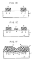
- a thermal oxide film 14 is grown, a phosphorus-doped polycrystalline silicon film 15 is deposited, and a resist film 16 is formed all after the field oxide films 6 are formed.
- the resist film 16 has portions formed on the edges of the polycrystalline silicon film 15 which respectively correspond to edges A of the field oxide films 6. These portions have a thickness greater than the remaining portions of the resist film 16. Therefore, when the resist film 16 is developed after exposure, residual resist portions 16' tend to be left at the edges of the field oxide film 6. Excessive development must be performed to remove these resist portions 16'. Therefore, controlling the size of the resist pattern is very difficult.
- the thickness (t 1 ) of the flat portion of the polycrystalline silicon film 15 is 4,000 A, but the thickness (t 2 ) of the stepped portion at each of the edges of the field oxide film 6 is about 9,000 A.
- the polycrystalline silicon film 15 is etched by the RIE method to micropattern the gate electrode to be formed, etching occurs only vertically downward from the surface.
- Fig. 3B residual polycrystalline silicon portions 17 are left at the stepped portions of the field oxide film 6.
- gate electrodes of the resultant MOS transistors are short-circuited because of the presence of these residual polycrystalline silicon portions 17.
- the semiconductor substrate comprises a p'- or n'-type semiconductor substrate, or a semiconductor structure consisting of the substrate and a monocrystalline semiconductor region formed thereon.
- the insulating film is used as a material for forming an element isolation region.
- the insulating film comprises a thermal oxide film, a CVD-Si0 2 film, a silicon nitride film or an alumina film.
- the portions of the semiconductor substrate which have an impurity concentration of at least 10 16 / CM 3 are not limited to the surface region covered with the element isolation layer, but extend to the whole of the semiconductor substrate.
- the level of the element region of the monocrystalline semiconductor layer is the same as that of the element isolation region.
- no resist pattern portions and no residual polycrystalline silicon portions remain and the disconnection of the aluminum wiring layer can be prevented.
- a semiconductor substrate with a high concentration (low resistance) is used, so that the change in substrate potential due to substrate current can be suppressed.
- step (b) There are two methods of performing step (b) as follows:
- a micropatterned element isolation layer can be formed with high precision.
- step (c) There are four methods of performing step (c) as follows:
- a polycrystalline silicon layer or an amorphous silicon layer can be used as the nonmonocrystalline semiconductor layer in methods (1) and (2).
- a laser or electron beam can be used as the energy beam.
- a micropatterned element isolation region can be formed by a simple process.
- the level of the element isolation region is the same as that of the element region of the monocrystalline semiconductor layer, no resist pattern portions in the vicinity of the edges of the element isolation region and no polycrystalline silicon film remain, and the disconnection of the aluminum wiring can be prevented.
- the semiconductor substrate has a high concentration (low resistance)
- the channel stopper under the element isolation region can be omitted. At the same time, the change in substrate potential due to the current flowing through the base (substrate) can be suppressed, thereby producing a high-performance semiconductor device.
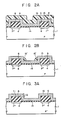
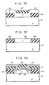
- the element region 108 of p-type monocrystalline silicon can be simply formed in the portion of the p*-type silicon substrate 101 which is surrounded by and is at the same level as the element isolation region 104.
- a step will not be formed between the element isolation region 104 and the element region 108 formed on the substrate. Therefore, the element region 108 can be smoothened with respect to the element isolation region 104. For this reason, after the oxide film 110 is formed and the phophorus-doped polycrystalline silicon film is formed in step (iv), the residual resist portions will not be left at the edges of the element isolation region 104 at the time of resist film application and photoengraving.
- a high precision resist pattern can be formed, and hence the gate electrode 109 can also be formed with high precision.
- step (iv) when the phosphorus-doped polycrystalline silicon film is deposited and is selectively etched by reactive ion etching using the resist pattern as a mask, the element isolation region 104 is at the same level as that of the element region 108 of p-type monocrystalline silicon, so that the residual polycrystalline silicon portions after etching will not be left at the element region 108 in the vicinity of the edges of the element isolation region 104.
- a highly reliable MOS-type semiconductor device can be prepared wherein a short circuit is not formed between the gate electrode 109, and the source and drain regions 111 and 112.
- the source and drain aluminum wiring patterns 114 and 115 are formed, disconnection of the aluminum wiring patterns 114 and 115 at the edges of the element isolation region 104 does not occur.
- the bird's beak can be eliminated, so that the element isolation region 104 can be micropatterned, and hence the element region 108 can also be micropatterned.
- an MOS-type semiconductor device having a high packing density can be obtained.
- the channel stopper can be automatically formed under the element isolation region 104, thereby omitting the need for a special formation process.
- the change in substrate potential due to a substrate current can be controlled. Therefore, an MOS-type semiconductor device having a stable threshold voltage can be obtained.
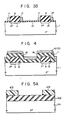
- the polycrystalline silicon layer is etched back such that the plasma nitride film is left by the RIE in the recess of the monocrystalline silicon layer, and the residual plasma nitride film and the monocrystalline silicon layer are simultaneously etched.
- formation of the polycrystalline silicon layer is not limited to this etch-back method.
- the resist film is sequentially etched. Thereafter, the exposed monocrystalline silicon layer on the element isolation region and the resist film are simultaneously etched.
- Example 2 produces the same effect as in Example 1. Furthermore, a micropatterned element isolation region having the same size as that of the resist pattern can be formed.
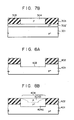
- Example 3 since a semiconductor substrate is used wherein the p-type monocrystalline silicon film 302 is grown on the p T- type silicon substrate 301, a high concentration of the monocrystalline silicon layer as the element region 304 can be prevented by the p-type monocrystalline silicon film 302 since boron will not be diffused from the substrate 301 to the element region 304.
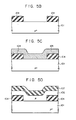
- the silicon film on the p + -type monocrystalline silicon substrate 301 was converted to a p +- type monocrystalline silicon film 302', as shown in Fig. 7B.
- boron may be further diffused from the p"-type silicon substrate 301 in the subsequent annealing process. Therefore, the channel stopper can be automatically formed under the element isolation region 303, and the concentration of boron in the element region 304 can be controlled.
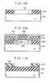
- a groove 403 is formed in the region of the substrate 401 which corresponds to the monocrystalline silicon layer.
- a p--type region 404a inversion preventive region of the element isolation region 402 can be formed only under and at the side surfaces of the p-type monocrystalline silicon layer404 (element region). Therefore, a p-type region 404b can be formed in the upper portion of the p-type monocrystalline silicon layer.
- the width I of the upper portion of the element isolation region 502 can be narrowed, and a micropatterned region can be obtained.
- the width L of the lower portion of the element isolation region 502 is wide, so that the short-channel effect of a field parasitic MOS transistor can be prevented.
- the etch-back method is performed such that the plasma nitride film is deposited and etched by RIE to leave the residual plasma nitride film in the recess of the polycrystalline silicon layer, and the residual plasma nitride film and the polycrystalline silicon layer are simultaneously etched back.
- another etch-back method may be adopted.
- a resist film may be formed on the pblycrystalline silicon layer having a groove such that the surface of the resist film becomes flat. Thereafter, the resist film is sequentially etched, and the exposed polycrystalline silicon layer portion on the element isolation region and the resist film are simultaneously etched back.
- Example 7 was substantially the same as Example 2 except that an element region was formed in the same manner as in Example 6, thereby producing an n-channel MOS-type semiconductor device.
- Example 6 the same effect as in Example 6 could be obtained.
- a micropatterned element isolation region having the same size as that of the resist film can be formed.
- Example 8 was substantially the same as Example 3 except that an element region was formed in the same manner as in Example 6, thereby producing an n-channel MOS-type semiconductor device. The same effect as in Example 3 could be obtained.
- Example 9 was substantially the same as Example 4 except that an element region was formed in the same manner as in Example 6, thereby producing an n-channel MOS-type semiconductor device. The same effect as in Example 4 could be obtained.
- Example 10 was substantially the same as Example 5 except that an element region was formed in the same manner as in Example 6, thereby producing an n-channel MOS-type semiconductor device. The same effect as in Example 5 could be obtained.
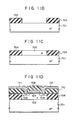
- a polycrystalline silicon film 803 was deposited by the CVD method to cover the entire surface (Fig. 12A).
- the polycrystalline silicon film 803 was selectively etched by reactive ion etching (RIE) to leave polycrystalline silicon portions on the side surfaces of the element isolation region 802, thereby obtaining residual polycrystalline silicon films 804 (Fig. 12B).
- RIE reactive ion etching
- a p-type monocrystalline silicon layer (element region) can be epitaxially grown on the island region of the substrate 801 (which was surrounded by the element isolation region 802) with good adhesion with the element isolation region 802.
- the diffusion rate of an impurity in the polycrystalline silicon patterns on the side surfaces of the element isolation region 802 is greater than that in the monocrystalline silicon layer, so that boron can be diffused from the p'- type silicon substrate 801 only to the polycrystalline silicon patterns 804 which can be used as inversion preventive layers.
- Example 13 was substantially the same as Example 2 except that an element region was formed in the same manner as in Example 11, thereby producing an n-channel MOS-type semiconductor device.
- Example 11 the same effect as in Example 11 can be obtained.
- a micropatterned element isolation region having the same size as the resist film can be obtained.
- Example 14 was substantially the same as Example 3 except that an element region was formed in the same manner as in Example 11, thereby producing an n-channel MOS-type semiconductor device. The same effect as in Example 3 could be obtained.
- Example 15 was substantially the same as Example 4 except that an element region was formed in the same manner as in Example 11, thereby producing an n-channel MOS-type semiconductor device. The same effect as in Example 4 could be obtained.
- Example 16 was substantially the same as Example 5 except that an element region was formed in the same manner as in Example 11, thereby producing an n-channel MOS-type semiconductor device. The same effect as in Example 5 could be obtained.
- Example 2 the same effect as in Example 1 could be obtained.
- Polycrystalline silicon films were formed on the side surfaces of the element isolation region in the same manner as Example 12, and on the element region in the same manner as in Example 17. In this Example, the same effect as in Example 12 could be obtained.
- Example 19 was substantially the same as Example 2 except that an element region was formed in the same manner as in Example 17, thereby producing an n-channel MOS-type semiconductor device.
- Example 17 the same effect as in Example 17 could be obtained.
- a micropatterned element isolation region having the same size as the resist film could be obtained.
- Example 20 was substantially the same as Example 3 except that an element region was formed in the same manner as in Example 17, thereby producing an n-channel MOS-type semiconductor device. The same effect as in Example 3 could be obtained.
- Example 21 was substantially the same as Example 4 except that an element region was formed in the same manner as in Example 17, thereby producing an n-channel MOS-type semiconductor device. The same effect as in Example 4 could be obtained.
- Example 16 was substantially the same as Example 5 except that an element region was formed in the same manner as in Example 17, thereby producing an n-channel MOS-type semiconductor device. The same effect as in Example 5 could be obtained.
- a p-type monocrystalline silicon layer may be formed and annealed after the boron-doped Si0 2 element isolation region is formed, so that a p'-type inversion preventive layer may be formed by diffusing boron from the element isolation region to the opposing side walls of the monocrystalline silicon layer.
- the boron-doped Si0 2 region can be formed by a method wherein a boron-doped Si0 2 film is patterned, or a method in which boron is ion-implanted in the side surfaces of an Si0 2 element isolation region. In particular, according to the latter method, ion implantation need not be performed when the side surfaces of the element isolation region of Fig. 9 are tapered.
- Ions can be vertically ion-implanted, thereby simplifying ion implantation.
- boron may be ion-implanted in the monocrystalline silicon layer. Therefore, boron can be directly doped in the portions of the monocrystalline silicon layer which are located at the side walls of the element isolation region.
- the p-type monocrystalline silicon layer serving as the element region has the same thickness as that of the element isolation region.
- the thickness of the p-type monocrystalline silicon layer need not be set to be the above-mentioned thickness.
- the thickness of the p-type monocrystalline silicon layer can be greater than that of an element isolation region 1002 to obtain an element region 1003.
- the thickness of the p-type monocrystalline silicon layer can be smaller than that of an element isolation region 1102 to obtain an element region 1103.
- the present invention is not limited to the manufacture of an n-channel MOS-type semiconductor device, but can be extended to the manufacture of a CMOS, a MNOS, a MAOS, or a MES semiconductor device, or an ECL or 1 2 L device.
- an element isolation region is formed on a semiconductor base (substrate), and the element region of a monocrystalline semiconductor layer formed on the semiconductor substrate portion surrounded by the element isolation region is at substantially the same level as that of the element isolation region. Residual resist portions at the edges of the element isolation region, residual gate electrode material, and the disconnection of the aluminum wiring layer can all be prevented. In addition, the change in substrate potential due to the substrate current can be prevented since the substrate has a high impurity concentration. Therefore, a highly integrated and reliable semiconductor device can be prepared. According to the method of the present invention, a micropatterned element isolation region can be obtained by a simple process. In addition, a channel stopper is automatically formed under the element isolation region due to the high impurity concentration in the substrate, thereby making a specific manufacturing process unnecessary. Therefore, high-perforance semiconductor devices can be manufactured in a mass production line.
Landscapes
- Element Separation (AREA)
Claims (21)
Applications Claiming Priority (8)
| Application Number | Priority Date | Filing Date | Title |
|---|---|---|---|
| JP58070426A JPS59195840A (ja) | 1983-04-21 | 1983-04-21 | 半導体装置の製造方法 |
| JP58070428A JPS59195842A (ja) | 1983-04-21 | 1983-04-21 | 半導体装置の製造方法 |
| JP70428/83 | 1983-04-21 | ||
| JP70426/83 | 1983-04-21 | ||
| JP58070427A JPS59195841A (ja) | 1983-04-21 | 1983-04-21 | 半導体装置の製造方法 |
| JP70427/83 | 1983-04-21 | ||
| JP76453/83 | 1983-04-30 | ||
| JP58076453A JPS59201440A (ja) | 1983-04-30 | 1983-04-30 | 半導体装置及びその製造方法 |
Publications (2)
| Publication Number | Publication Date |
|---|---|
| EP0126292A1 EP0126292A1 (fr) | 1984-11-28 |
| EP0126292B1 true EP0126292B1 (fr) | 1987-12-02 |
Family
ID=27465243
Family Applications (1)
| Application Number | Title | Priority Date | Filing Date |
|---|---|---|---|
| EP84104279A Expired EP0126292B1 (fr) | 1983-04-21 | 1984-04-16 | Dispositif semi-conducteur avec une couche d'isolement entre les éléments et procédé de fabrication |
Country Status (3)
| Country | Link |
|---|---|
| US (1) | US4755863A (fr) |
| EP (1) | EP0126292B1 (fr) |
| DE (1) | DE3467953D1 (fr) |
Families Citing this family (8)
| Publication number | Priority date | Publication date | Assignee | Title |
|---|---|---|---|---|
| US4908683A (en) * | 1986-03-19 | 1990-03-13 | Harris Corporation | Technique for elimination of polysilicon stringers in direct moat field oxide structure |
| JPH01185936A (ja) * | 1988-01-21 | 1989-07-25 | Fujitsu Ltd | 半導体装置 |
| US5045898A (en) * | 1988-08-30 | 1991-09-03 | At&T Bell Laboratories | CMOS integrated circuit having improved isolation |
| JPH0656865B2 (ja) * | 1988-10-13 | 1994-07-27 | 株式会社東芝 | 高耐圧素子用接着基板 |
| JPH03296247A (ja) * | 1990-04-13 | 1991-12-26 | Mitsubishi Electric Corp | 半導体装置およびその製造方法 |
| JPH0582465A (ja) * | 1991-09-24 | 1993-04-02 | Victor Co Of Japan Ltd | 半導体装置およびmos型fet |
| US8226772B2 (en) | 2009-01-08 | 2012-07-24 | Micron Technology, Inc. | Methods of removing particles from over semiconductor substrates |
| CN112269277B (zh) * | 2020-10-09 | 2024-03-22 | 厦门兴华鼎自动化技术有限公司 | 一种基于应力硅的电光调制器及其制备方法 |
Family Cites Families (17)
| Publication number | Priority date | Publication date | Assignee | Title |
|---|---|---|---|---|
| US3728161A (en) * | 1971-12-28 | 1973-04-17 | Bell Telephone Labor Inc | Integrated circuits with ion implanted chan stops |
| US3966501A (en) * | 1973-03-23 | 1976-06-29 | Mitsubishi Denki Kabushiki Kaisha | Process of producing semiconductor devices |
| JPS51135385A (en) * | 1975-03-06 | 1976-11-24 | Texas Instruments Inc | Method of producing semiconductor device |
| NL191683C (nl) * | 1977-02-21 | 1996-02-05 | Zaidan Hojin Handotai Kenkyu | Halfgeleidergeheugenschakeling. |
| JPS54881A (en) * | 1977-06-03 | 1979-01-06 | Fujitsu Ltd | Semiconductor device |
| US4514747A (en) * | 1978-08-07 | 1985-04-30 | Hitachi, Ltd. | Field controlled thyristor with double-diffused source region |
| DE2967388D1 (en) * | 1978-09-20 | 1985-03-28 | Fujitsu Ltd | Semiconductor memory device and process for fabricating the device |
| US4338622A (en) * | 1979-06-29 | 1982-07-06 | International Business Machines Corporation | Self-aligned semiconductor circuits and process therefor |
| US4441246A (en) * | 1980-05-07 | 1984-04-10 | Texas Instruments Incorporated | Method of making memory cell by selective oxidation of polysilicon |
| JPS5756961A (en) * | 1980-09-20 | 1982-04-05 | Ricoh Co Ltd | Complementary mos field effect semiconductor device |
| US4487639A (en) * | 1980-09-26 | 1984-12-11 | Texas Instruments Incorporated | Localized epitaxy for VLSI devices |
| US4331708A (en) * | 1980-11-04 | 1982-05-25 | Texas Instruments Incorporated | Method of fabricating narrow deep grooves in silicon |
| EP0061855B1 (fr) * | 1981-03-20 | 1985-08-14 | Kabushiki Kaisha Toshiba | Procédé de fabrication d'un élément semiconducteur |
| FR2505814A1 (fr) * | 1981-05-13 | 1982-11-19 | Air Liquide | Masse silico-calcaire a haute porosite et procede de preparation |
| JPS57204148A (en) * | 1981-06-10 | 1982-12-14 | Toshiba Corp | Manufacture of semiconductor device |
| US4637127A (en) * | 1981-07-07 | 1987-01-20 | Nippon Electric Co., Ltd. | Method for manufacturing a semiconductor device |
| US4412868A (en) * | 1981-12-23 | 1983-11-01 | General Electric Company | Method of making integrated circuits utilizing ion implantation and selective epitaxial growth |
-
1984
- 1984-04-16 DE DE8484104279T patent/DE3467953D1/de not_active Expired
- 1984-04-16 EP EP84104279A patent/EP0126292B1/fr not_active Expired
-
1986
- 1986-08-15 US US06/895,599 patent/US4755863A/en not_active Expired - Lifetime
Also Published As
| Publication number | Publication date |
|---|---|
| DE3467953D1 (en) | 1988-01-14 |
| EP0126292A1 (fr) | 1984-11-28 |
| US4755863A (en) | 1988-07-05 |
Similar Documents
| Publication | Publication Date | Title |
|---|---|---|
| EP0036082B1 (fr) | Procédé autoaligné pour la réalisation d'un transistor bipolaire à haute performance | |
| EP0146895B1 (fr) | Procédé pour la fabrication de dispositifs semi-conducteurs | |
| US4471525A (en) | Method for manufacturing semiconductor device utilizing two-step etch and selective oxidation to form isolation regions | |
| US4755481A (en) | Method of making a silicon-on-insulator transistor | |
| EP0051488A2 (fr) | Procédé de fabrication d'un dispositif semiconducteur | |
| US4994400A (en) | Method of fabricating a semiconductor device using a tri-layer structure and conductive sidewalls | |
| EP0055521B1 (fr) | Procédé de remplissage d'une rainure dans un substrat semiconducteur | |
| EP0224717B1 (fr) | Interrupteur de canal auto-aligné | |
| EP0070402B1 (fr) | Procédé pour former des configurations électroconductrices sur un dispositif semiconducteur, et un dispositif semiconducteur fabriqué par le procédé | |
| US4900689A (en) | Method of fabrication of isolated islands for complementary bipolar devices | |
| US4191595A (en) | Method of manufacturing PN junctions in a semiconductor region to reach an isolation layer without exposing the semiconductor region surface | |
| US4722908A (en) | Fabrication of a bipolar transistor with a polysilicon ribbon | |
| US4714685A (en) | Method of fabricating self-aligned silicon-on-insulator like devices | |
| JP2785919B2 (ja) | 絶縁層の上に成長層を有する半導体装置の製造方法 | |
| US4560421A (en) | Semiconductor device and method of manufacturing the same | |
| EP0326211B1 (fr) | Dispositif semi-conducteur et procédé de fabrication de ce dispositif | |
| US4755863A (en) | Semiconductor device having a semiconductor substrate with a high impurity concentration | |
| US4897698A (en) | Horizontal structure thin film transistor | |
| JPH06232247A (ja) | 絶縁層上に隔離された半導体層を製造する方法 | |
| JPH0324069B2 (fr) | ||
| JPH0974189A (ja) | 半導体装置の製造方法 | |
| JP3125429B2 (ja) | 半導体装置及びその製造方法 | |
| EP0180363B1 (fr) | Transistor de structure horizontale et son procédé de fabrication | |
| EP0236811B1 (fr) | Procédé pour la fabrication d'un dispositif à semi-conducteur | |
| US5686327A (en) | Method for fabricating semiconductor device |
Legal Events
| Date | Code | Title | Description |
|---|---|---|---|
| PUAI | Public reference made under article 153(3) epc to a published international application that has entered the european phase |
Free format text: ORIGINAL CODE: 0009012 |
|
| 17P | Request for examination filed |
Effective date: 19840416 |
|
| AK | Designated contracting states |
Designated state(s): DE FR GB IT |
|
| GRAA | (expected) grant |
Free format text: ORIGINAL CODE: 0009210 |
|
| AK | Designated contracting states |
Kind code of ref document: B1 Designated state(s): DE FR GB IT |
|
| ITF | It: translation for a ep patent filed | ||
| REF | Corresponds to: |
Ref document number: 3467953 Country of ref document: DE Date of ref document: 19880114 |
|
| ET | Fr: translation filed | ||
| PLBE | No opposition filed within time limit |
Free format text: ORIGINAL CODE: 0009261 |
|
| STAA | Information on the status of an ep patent application or granted ep patent |
Free format text: STATUS: NO OPPOSITION FILED WITHIN TIME LIMIT |
|
| 26N | No opposition filed | ||
| ITTA | It: last paid annual fee | ||
| PGFP | Annual fee paid to national office [announced via postgrant information from national office to epo] |
Ref country code: GB Payment date: 19970407 Year of fee payment: 14 |
|
| PGFP | Annual fee paid to national office [announced via postgrant information from national office to epo] |
Ref country code: FR Payment date: 19970409 Year of fee payment: 14 |
|
| PGFP | Annual fee paid to national office [announced via postgrant information from national office to epo] |
Ref country code: DE Payment date: 19970428 Year of fee payment: 14 |
|
| PG25 | Lapsed in a contracting state [announced via postgrant information from national office to epo] |
Ref country code: GB Free format text: LAPSE BECAUSE OF NON-PAYMENT OF DUE FEES Effective date: 19980416 |
|
| PG25 | Lapsed in a contracting state [announced via postgrant information from national office to epo] |
Ref country code: FR Free format text: THE PATENT HAS BEEN ANNULLED BY A DECISION OF A NATIONAL AUTHORITY Effective date: 19980430 |
|
| GBPC | Gb: european patent ceased through non-payment of renewal fee |
Effective date: 19980416 |
|
| PG25 | Lapsed in a contracting state [announced via postgrant information from national office to epo] |
Ref country code: DE Free format text: LAPSE BECAUSE OF NON-PAYMENT OF DUE FEES Effective date: 19990202 |
|
| REG | Reference to a national code |
Ref country code: FR Ref legal event code: ST |