EP0146895B1 - Procédé pour la fabrication de dispositifs semi-conducteurs - Google Patents
Procédé pour la fabrication de dispositifs semi-conducteurs Download PDFInfo
- Publication number
- EP0146895B1 EP0146895B1 EP84115477A EP84115477A EP0146895B1 EP 0146895 B1 EP0146895 B1 EP 0146895B1 EP 84115477 A EP84115477 A EP 84115477A EP 84115477 A EP84115477 A EP 84115477A EP 0146895 B1 EP0146895 B1 EP 0146895B1
- Authority
- EP
- European Patent Office
- Prior art keywords
- film
- oxide film
- oxidation
- substrate
- groove
- Prior art date
- Legal status (The legal status is an assumption and is not a legal conclusion. Google has not performed a legal analysis and makes no representation as to the accuracy of the status listed.)
- Expired
Links
Images



Classifications
-
- H—ELECTRICITY
- H10—SEMICONDUCTOR DEVICES; ELECTRIC SOLID-STATE DEVICES NOT OTHERWISE PROVIDED FOR
- H10W—GENERIC PACKAGES, INTERCONNECTIONS, CONNECTORS OR OTHER CONSTRUCTIONAL DETAILS OF DEVICES COVERED BY CLASS H10
- H10W10/00—Isolation regions in semiconductor bodies between components of integrated devices
- H10W10/10—Isolation regions comprising dielectric materials
- H10W10/17—Isolation regions comprising dielectric materials formed using trench refilling with dielectric materials, e.g. shallow trench isolations
-
- H—ELECTRICITY
- H10—SEMICONDUCTOR DEVICES; ELECTRIC SOLID-STATE DEVICES NOT OTHERWISE PROVIDED FOR
- H10P—GENERIC PROCESSES OR APPARATUS FOR THE MANUFACTURE OR TREATMENT OF DEVICES COVERED BY CLASS H10
- H10P76/00—Manufacture or treatment of masks on semiconductor bodies, e.g. by lithography or photolithography
- H10P76/40—Manufacture or treatment of masks on semiconductor bodies, e.g. by lithography or photolithography of masks comprising inorganic materials
- H10P76/405—Manufacture or treatment of masks on semiconductor bodies, e.g. by lithography or photolithography of masks comprising inorganic materials characterised by their composition, e.g. multilayer masks
-
- H—ELECTRICITY
- H10—SEMICONDUCTOR DEVICES; ELECTRIC SOLID-STATE DEVICES NOT OTHERWISE PROVIDED FOR
- H10P—GENERIC PROCESSES OR APPARATUS FOR THE MANUFACTURE OR TREATMENT OF DEVICES COVERED BY CLASS H10
- H10P76/00—Manufacture or treatment of masks on semiconductor bodies, e.g. by lithography or photolithography
- H10P76/40—Manufacture or treatment of masks on semiconductor bodies, e.g. by lithography or photolithography of masks comprising inorganic materials
- H10P76/408—Manufacture or treatment of masks on semiconductor bodies, e.g. by lithography or photolithography of masks comprising inorganic materials characterised by their sizes, orientations, dispositions, behaviours or shapes
- H10P76/4085—Manufacture or treatment of masks on semiconductor bodies, e.g. by lithography or photolithography of masks comprising inorganic materials characterised by their sizes, orientations, dispositions, behaviours or shapes characterised by the processes involved to create the masks
-
- H—ELECTRICITY
- H10—SEMICONDUCTOR DEVICES; ELECTRIC SOLID-STATE DEVICES NOT OTHERWISE PROVIDED FOR
- H10P—GENERIC PROCESSES OR APPARATUS FOR THE MANUFACTURE OR TREATMENT OF DEVICES COVERED BY CLASS H10
- H10P76/00—Manufacture or treatment of masks on semiconductor bodies, e.g. by lithography or photolithography
- H10P76/40—Manufacture or treatment of masks on semiconductor bodies, e.g. by lithography or photolithography of masks comprising inorganic materials
- H10P76/408—Manufacture or treatment of masks on semiconductor bodies, e.g. by lithography or photolithography of masks comprising inorganic materials characterised by their sizes, orientations, dispositions, behaviours or shapes
- H10P76/4088—Processes for improving the resolution of the masks
-
- H—ELECTRICITY
- H10—SEMICONDUCTOR DEVICES; ELECTRIC SOLID-STATE DEVICES NOT OTHERWISE PROVIDED FOR
- H10W—GENERIC PACKAGES, INTERCONNECTIONS, CONNECTORS OR OTHER CONSTRUCTIONAL DETAILS OF DEVICES COVERED BY CLASS H10
- H10W10/00—Isolation regions in semiconductor bodies between components of integrated devices
- H10W10/01—Manufacture or treatment
- H10W10/011—Manufacture or treatment of isolation regions comprising dielectric materials
- H10W10/012—Manufacture or treatment of isolation regions comprising dielectric materials using local oxidation of silicon [LOCOS]
- H10W10/0125—Manufacture or treatment of isolation regions comprising dielectric materials using local oxidation of silicon [LOCOS] comprising introducing electrical impurities in local oxidation regions, e.g. to alter LOCOS oxide growth characteristics
- H10W10/0126—Manufacture or treatment of isolation regions comprising dielectric materials using local oxidation of silicon [LOCOS] comprising introducing electrical impurities in local oxidation regions, e.g. to alter LOCOS oxide growth characteristics introducing electrical active impurities in local oxidation regions to create channel stoppers
-
- H—ELECTRICITY
- H10—SEMICONDUCTOR DEVICES; ELECTRIC SOLID-STATE DEVICES NOT OTHERWISE PROVIDED FOR
- H10W—GENERIC PACKAGES, INTERCONNECTIONS, CONNECTORS OR OTHER CONSTRUCTIONAL DETAILS OF DEVICES COVERED BY CLASS H10
- H10W10/00—Isolation regions in semiconductor bodies between components of integrated devices
- H10W10/01—Manufacture or treatment
- H10W10/011—Manufacture or treatment of isolation regions comprising dielectric materials
- H10W10/014—Manufacture or treatment of isolation regions comprising dielectric materials using trench refilling with dielectric materials, e.g. shallow trench isolations
- H10W10/0148—Manufacture or treatment of isolation regions comprising dielectric materials using trench refilling with dielectric materials, e.g. shallow trench isolations comprising introducing impurities in side walls or bottom walls of trenches, e.g. for forming channel stoppers
-
- H—ELECTRICITY
- H10—SEMICONDUCTOR DEVICES; ELECTRIC SOLID-STATE DEVICES NOT OTHERWISE PROVIDED FOR
- H10W—GENERIC PACKAGES, INTERCONNECTIONS, CONNECTORS OR OTHER CONSTRUCTIONAL DETAILS OF DEVICES COVERED BY CLASS H10
- H10W10/00—Isolation regions in semiconductor bodies between components of integrated devices
- H10W10/10—Isolation regions comprising dielectric materials
- H10W10/13—Isolation regions comprising dielectric materials formed using local oxidation of silicon [LOCOS], e.g. sealed interface localised oxidation [SILO] or side-wall mask isolation [SWAMI]
Definitions
- the present invention relates to a method of manufacturing a semiconductor device and, more particularly, to a method of forming a micro-patterned field region in a semiconductor device.
- a thermal oxide film 2 having a thickness of about 90nm (900 ⁇ ) is formed on a p ⁇ -type silicon substrate 1 having a plane (100).
- a polycrystalline silicon film 3 with a thickness of about 500 ⁇ and a silicon nitride film 4 with a thickness of about 2,500 ⁇ are sequentially formed on the thermal oxide film 2.
- a resist film is then formed on the silicon nitride film 4 and is patterned by photolithography, thereby forming a resist pattern 5 having an opening corresponding to a prospective field region of the silicon substrate 1.
- the silicon nitride film 4 is selectively removed by reactive ion etching using the resist pattern 5 as a mask.
- An impurity 8 for preventing inversion is ion-implanted in the silicon substrate 1 through the polycrystalline silicon film 3 and the thermal oxide film 2 from the thus formed opening 6.
- boron can be used as the impurity and the irradiating condition can be an accelerating energy of 100 KeV and a dose of 1 x 1013 cm ⁇ 2.
- the resultant structure is subjected to thermal oxidation in an oxidizing atmosphere using the residual silicon nitride film 4 as an oxidation-resistive mask so as to form a field oxide film 9 with a thickness of about 8,000 ⁇ , as shown in Fig. 1C.
- the impurity 8 for preventing inversion is diffused to form a field inversion layer 10 immediately under the field oxide film 9.
- the field oxide film 9 undesirably extends along the lateral direction thereof by about 0.7 ⁇ m.
- the resist film has a resolution limit of about 1.2 ⁇ m. Therefore, a micro-patterned field oxide film having a width of 1.9 ⁇ m or less cannot be obtained.
- a first thermal oxide film 12 having a thickness of 1,000 ⁇ is formed on a p ⁇ -type silicon substrate 11 having a plane (100).
- a photoresist pattern 13 is formed on an element forming region.
- an impurity for preventing field inversion e.g., B+
- B+ an impurity for preventing field inversion
- the first thermal oxide film 12 is selectively etched using the photoresist pattern 13 as a mask.
- boron in the boron-doped layer 14 is diffused by a heat treatment, thereby forming a p-type impurity region 15 as a field inversion preventive layer (Fig. 2B).
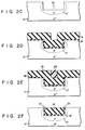
- the substrate 11 is etched to a depth of about 6,000 ⁇ using the residual first thermal oxide film 12 as a mask so as to form a groove 16, and to form a p-type field inversion preventive layer 17 in a portion which constitutes the groove 16.
- the residual first thermal oxide film 12 is removed (Fig. 2C).
- a second thermal oxide film 18 with a thickness of about 500 ⁇ is formed on a surface of the substrate 11 including an inner surface of the groove 6.
- a CVD oxide film 19 is deposited on the overall surface of the resultant structure to a thickness of 6,000 ⁇ (Fig. 2D).
- the photoresist is etched by reactive ion etching so as to leave a photoresist pattern 20 in a recessed portion of the CVD oxide film 19 corresponding to a shape of the groove 16 (Fig. 2E).
- the remaining photoresist pattern 20, the CVD oxide film 19 and the second thermal oxide film 18 are simultaneously etched by reactive ion etching so as to expose the substrate 11.
- the CVD oxide film 19 is buried in the groove of the substrate 11, thus forming an element isolation region (Fig. 2F).
- MOS semiconductor element is formed in an element region surrounded by the CVD oxide film 19 in a conventional manner, thereby obtaining a MOS semiconductor device.
- the element isolation technique of the buried isolation type as described above has the following disadvantages.
- boron is ion-implanted using the photoresist pattern 13 as a mask so as to form the boron-doped layer 14, and in the process of Fig. 2B, the boron of the boron-doped layer 14 is diffused by annealing, thereby forming the p-type impurity region 15. Thereafter, in the process of Fig. 2C, the substrate 11 is etched to form the groove 16, and the p-type field inversion preventive layer 17 is formed in the portion which constitutes the groove 16.
- a field inversion preventive layer having a higher concentration than that of the substrate 11 is not formed.
- n+-type source and drain regions of the MOS transistor are formed in the element region after forming the element isolation region by burying the CVD oxide film 19 in the groove of the substrate 11 in the process up to Fig. 2F, a junction-leakage current easily flows at the field edges 21, resulting in the degradation in electrical characteristics of the device.
- US-A-4 407 696 describes a method of fabricating an isolation oxide film or field oxide to separate active or element regions on the surface of an MOS integrated circuit.
- On the surface of a semiconductor substrate there are fabricated in successive layers an oxide layer, a polysilicon layer and a nitride layer.
- a patterned resist layer is formed on the surface of the nitride layer and the nitride layer is etched through an opening in the resist layer.
- Ion implantation is carried out in the patterned opening in the nitride layer into the substrate through the polysilicon layer and the oxide layer.
- the ions have insufficient energy to penetrate the combined layers of the resist layer, nitride layer, polysilicon layer and oxide layer.
- the implantation is therefore only applied in the area of the substrate exposed by the opening. Implantation into areas on either side of the opening, which are reserved for element areas, is thus inhibited.
- the isolation oxidation is then grown through the opening in the nitride layer.
- the isolation oxide comprises oxide derived from the oxide layer and from oxide produced from the polysilicon layer and the semiconductor substrate.
- the resulting field oxide layer has a reduced "bird's beak" area.
- a silicon substrate is covered by a first oxide layer and a second nitride layer.
- a thick polysilicon layer is then applied and patterned to form an opening.
- the polysilicon layer is oxidised, by which process the opening is reduced in size by lateral expansion. The process can be controlled to vary the dimensions of the opening as required.
- the nitride and oxide layer in the opening are etched to expose the substrate.
- the exposed substrate may be etched before oxidation to form a recessed oxide region.
- the object of the present invention is solved by a method of manufacturing a semiconductor device, comprising the steps of: (a) sequentially forming an oxidation-resistive film and an oxidizable film on a semiconductor substrate; (b) forming a window in a predetermined region of said oxidizable film, in which said oxidation-resistive film is exposed; (c) after step, introducing an impurity of the same conductivity type as that of said semiconductor substrate into said semiconductor substrate using said oxidizable film as a mask; (d) applying thermal oxidation to said oxidizable film so as to convert said oxidizable film into an insulating film and to decrease a width of said window by volume expansion due to the conversion and to diffuse said impurity into said substrate; (e) forming a field oxide film in a region of said semiconductor substrate defined by said window of said insulating film comprising the steps of forming a groove in said semiconductor substrate by selectively removing said oxidation-resistive film and said
- step (a) if the oxidation-resistive film were to be directly formed on the surface of the substrate, a so-called “white ribbon” may occur in the surface of the substrate in the thermal oxidation of step (c), thereby degrading element properties. Therefore, a thermal oxide film is preferably formed on the surface of the substrate.
- the method of burying the oxide film in the groove comprises the steps of selectively removing the oxidation-resistive film and the semiconductor substrate using the insulating film as a mask so as to form a groove in the substrate, and filling the groove with an oxide film.
- the oxide film is deposited on the overall surface of the structure, including that of the groove, by a CVD method.
- the groove in the oxide film which is formed to correspond to the groove in the substrate is filled with a resist film, and the overall surface of the structure is etched until the surface of the substrate is exposed. If the CVD film is in direct contact with the substrate, there is the risk of degrading the element properties.
- a thermal oxide film is preferably formed on the overall surface of the substrate including the groove.
- an impurity of the same conductivity type as that of the substrate can be selectively doped in the substrate using the oxidizable film as a mask.
- the impurity is diffused and activated in the thermal oxidation process, thereby forming an inversion preventive layer under the field oxide film. Since the impurity is introduced before the thermal oxidation, that is, before the width of the window of the oxidizable film is decreased, an impurity region can be widened. For this reason, the inversion preventive layer can be reliably formed in a peripheral portion of the field oxide film, more particularly, a portion on the surface of the substrate.
- a silicon nitride film can be used as the oxidation-resistive film, and a metal silicide such as a polycrystalline silicon, molybdenum silicide or the like can be used as the oxidizable film.
- a micro-patterned field oxide film can be easily formed.
- the field inversion preventive layer can be reliably formed. Therefore, current leakage in a p-n junction can be effectively prevented.
- Example 1 a field region is formed using a selective oxidation method, and in Example 2, a field region is formed by burying an insulating layer in a groove provided in a substrate.
- a first insulating film 31 which is formed of a thermal oxide film having a thickness of about 900 ⁇ is formed on a p ⁇ -type silicon substrate 30 having a plane (100).
- a first oxidizable film 32 formed of a polycrystalline silicon film with a thickness of about 500 ⁇ and an oxidation-resistive film 33 formed of a silicon nitride film with a thickness of 2,500 ⁇ are sequentially formed on the first insulating film 31.
- a second oxidizable film 34 formed of a polycrystalline silicon film with a thickness of 3,500 ⁇ is formed on the oxidation-resistive film 33.
- the first oxidizable film 32 and the oxidation-resistive film 33 can be formed by a low-temperature CVD method.
- a resist film (not shown) having a window at a region corresponding to a prospective field region is placed in the second oxidizable film 34.
- a window 35 is formed in the second oxidizable film 34 by reactive ion etching using the resist film as a mask.
- the resultant structure is subjected to thermal oxidation in a combusting, oxidizing atmosphere, thereby converting the second oxidizable film 34 into a second insulating film 36 of about 7,000 ⁇ in thickness.
- the second oxidizable film 34 is converted into the second insulating film 36, volume expansion occurs.
- the extent of the volume expansion is set such that a window 37, which will be formed in an oxidation-resistive film 33 in a later step, is reduced and cancels the lateral extension of a field oxide film 39, which will also be formed in the later process.
- the window 37 is formed in the oxidation-resistive film 33 using the second insulating film 36 as a mask.
- An impurity 38 for preventing inversion is ion-implanted in the silicon substrate 30 through the window 37, the first oxidizable film 32 and the first insulating film 31.
- B+ is used as the impurity 38, and ion-implantation conditions are set to be an acceleration energy of 100 KeV and a dose of about 1 x 1013 cm ⁇ 2.
- the second insulating film 36 is removed.
- the silicon substrate 30 is subjected to thermal oxidation in a combusting, oxidizing atmosphere using the residual oxidation-resistive film 33 as a mask so as to form the field oxide film 39 having a thickness of about 8,000 ⁇ .
- the impurity 38 is diffused and activated by this annealing, thereby forming a field inversion preventive layer 40 immediately under the field oxide film 39.
- the oxidation-resistive film 33 and the first oxidizable film 32 are removed. Thereafter, an element region isolated by the field oxide film 39 is subjected to an impurity diffusion process and the like, thus forming a semiconductor element which satisfies predetermined requirements.
- a volume expansion coefficient of the film can be set so that the lateral extension of the field oxide film 39 can be cancelled by a decrease in the a diameter of the window 35.
- the field oxide film 39 can be formed by utilizing the window 37 of the oxidation-resistive film 33 formed in accordance with the window 35, thereby achieving micro-patterning.
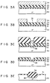
- a first thermal oxide film 42 is formed on a surface of a p ⁇ -type silicon substrate 41 having a plane (100) so as to have a thickness of about 500 ⁇ .
- a silicon nitride film (oxidation-resistive film) 43 having a thickness of about 500 ⁇ and a polycrystalline silicon film (oxidizable film) 44 having a thickness of about 2,000 ⁇ are sequentially deposited on the first thermal oxide film 42 (Fig. 4A).
- a photoresist pattern 45 which has an opening wider than a final element isolation width is formed on an element region forming portion. Thereafter, the polycrystalline silicon film 44 is etched by reactive ion etching using the pattern 45 as a mask.
- an impurity for preventing field inversion e.g., B+
- an impurity for preventing field inversion e.g., B+
- an impurity for preventing field inversion e.g., B+
- an acceleration energy of 100 KeV and a dose of 3 x 1013 cm ⁇ 2 using the photoresist pattern 45 as a mask, thereby forming a boron-doped layer 46 (Fig. 4B).
- the resultant structure is subjected to thermal oxidation in a combusting oxidizing atmosphere, so that the polycrystalline silicon film 44 is converted into a second thermal oxide film 47, thus expanding the volume thereof.
- the doped boron in the boron-doped layer 46 is diffused, thereby forming a p-type impurity region 48 as a field inversion preventive layer (Fig. 4C).
- the silicon nitride film 43 and the first thermal oxide film 42 are sequentially etched using the second thermal oxide film 47 as a mask, and furthermore, the substrate 41 is etched to a depth of about 6,000 ⁇ , thereby forming a groove 49. Then, a p-type field inversion preventive layer 50 is formed in a portion which defines the groove 49 (Fig. 4D).
- the second thermal oxide film 47, the silicon nitride film 43 and the first thermal oxide film 42 are sequentially removed by etching (Fig. 4E).
- a third thermal oxide film 51 is formed on a surface of the substrate 41 including the groove 49 so as to have a thickness of about 500 ⁇ .
- a CVD oxide film 52 having a thickness of about 6,000 ⁇ is deposited on the overall surface of the resultant structure (Fig. 4F).
- the photoresist pattern is etched by reactive ion etching so that a photoresist 53 remains in a recessed portion of the CVD oxide film 52 corresponding to a shape of the groove 49 (Fig. 4G).
- the residual photoresist 53, the CVD oxide film 52 and the third thermal oxide film 51 are simultaneously etched to expose the surface of the substrate 41 by reactive ion etching.
- the CVD oxide film 52 is buried in the groove 49 through the third thermal oxide film 51, thereby forming an element isolation region (Fig. 4H).
- MOS semiconductor element is formed in an element region surrounded by the CVD oxide film 52 in accordance with a conventional process.
- boron for preventing field inversion is ion-implanted using the oxidizable film (polycrystalline silicon film 44) as a mask which has an opening wider than the final element isolation width.
- the polycrystalline silicon film 44 is thermally oxidized, thereby forming the second thermal oxide film 47.
- the volume of the polycrystalline silicon film 44 is expanded so that the opening thereof becomes the same as the final element isolation width, and the doped boron is then diffused, thereby forming the p-type impurity region as the field inversion preventive layer.
- the field inversion preventive layer 50 can also be formed in a major surface of the substrate 41 to finally be a field edge.
- the CVD oxide film 52 is formed in the groove 49 through the thermal oxide film 51, thereby forming the element isolation region. Thereafter, even if, for example, n+-type source and drain regions of a MOS transistor are formed in the element region surrounded by the CVD oxide film 52, a p-n junction with the p-type field inversion preventive layer 50 is provided, thereby reducing a junction leakage current.
- the first thermal oxide film 42 is formed on the substrate 41 before forming the silicon nitride film 43 as the oxidation-resistive film. er, the first thermal oxide film 42 can be omitted. However, in this case, if the thermal oxide film is not formed under the silicon nitride film 43, white ribbon may be formed in the surface of the substrate 41 in thermal oxidation of the polycrystalline silicon film 44, resulting in a degradation of the element properties. Therefore, the thermal oxide film is preferably formed under the silicon nitride film 43.
- the third thermal oxide film 51 is formed on the surface of the substrate 41 including the groove 49 before forming the CVD oxide film 52.
- the third thermal oxide film can be omitted.
- the third thermal oxide film is preferably formed.
Landscapes
- Element Separation (AREA)
- Local Oxidation Of Silicon (AREA)
Claims (5)
- Procédé de fabrication d'un dispositif à semi-conducteur, comprenant les étapes suivantes :(a) la formation successive d'un film résistant à l'oxydation (43) et d'un film oxydable (44) sur un substrat semi-conducteur (41),(b) la formation d'une fenêtre dans une région prédéterminée du film oxydable (44) dans laquelle le film résistant à l'oxydation (43) est exposé,(c) après l'étape (b), l'introduction d'une impureté (B+) du même type de conductivité que le substrat semi-conducteur (41), dans le substrat semi-conducteur (41) avec utilisation du film oxydable (44) comme masque,(d) l'application d'une oxydation thermique au film oxydable (44) afin que le film oxydable (44) se transforme en un film igolant (47), que la largeur de la fenêtre diminue du fait de la dilatation en volume due à la conversion, et que l'impureté diffuse dans le substrat,(e) la formation d'un film d'oxyde de champ (52) dans une région du substrat semi-conducteur (41) délimitée par la fenêtre du film isolant (47), comprenant des étapes de formation d'une gorge (49) dans le substrat semi-conducteur (41) par extraction sélective du film résistant à l'oxydation (43) et du substrat semi-conducteur (41) avec le film isolant (47) comme masque, avec enlèvement du film isolant (47) et du film résistant à l'oxydation (43), et(f) le dépôt d'un film d'oxyde (52) sur toute la surface du substrat semi-conducteur (41) y compris la gorge (49), avec enfouissement d'une autre gorge dans le film d'oxyde (52) qui est formée d'une manière correspondant à la gorge (49) du substrat (41) avec un film d'un matériau de réserve (53) et par traitement de toute la surface par une attaque, et(g) la formation d'un élément semi-conducteur dans la région du substrat semi-conducteur (41) qui est isolée par le film d'oxyde de champ (52).
- Procédé selon la revendication 1, caractérisé on ce que, dans l'étape (a), un film d'oxyde thermique (42) est formé sur le substrat semi-conducteur (41) avant la formation du fila résistant à l'oxydation (43).
- Procédé selon l'une des revendications 1 et 2, caractérisé en ce qu'un autre film d'oxyde thermique (51) est formé sur toute la surface du substrat semi-conducteur (41), y compris la gorge (49), avant enfouissement dans la gorge (49) par le film d'oxyde (52).
- Procédé selon la revendication 1, caractérisé en ce que le film résistant à l'oxydation (43) est formé de nitrure de silicium.
- Procédé selon la revendication 1, caractérisé en ce que le film oxydable (44) est formé d'un matériau choisi dans le groupe qui comprend le silicium polycristallin et un siliciure métallique.
Applications Claiming Priority (4)
| Application Number | Priority Date | Filing Date | Title |
|---|---|---|---|
| JP58237357A JPS60128636A (ja) | 1983-12-16 | 1983-12-16 | 半導体装置の製造方法 |
| JP237357/83 | 1983-12-16 | ||
| JP93184/84 | 1984-05-10 | ||
| JP59093184A JPS60236247A (ja) | 1984-05-10 | 1984-05-10 | 半導体装置の製造方法 |
Publications (3)
| Publication Number | Publication Date |
|---|---|
| EP0146895A2 EP0146895A2 (fr) | 1985-07-03 |
| EP0146895A3 EP0146895A3 (en) | 1988-02-17 |
| EP0146895B1 true EP0146895B1 (fr) | 1992-08-19 |
Family
ID=26434611
Family Applications (1)
| Application Number | Title | Priority Date | Filing Date |
|---|---|---|---|
| EP84115477A Expired EP0146895B1 (fr) | 1983-12-16 | 1984-12-14 | Procédé pour la fabrication de dispositifs semi-conducteurs |
Country Status (3)
| Country | Link |
|---|---|
| US (1) | US4570325A (fr) |
| EP (1) | EP0146895B1 (fr) |
| DE (1) | DE3485880T2 (fr) |
Families Citing this family (52)
| Publication number | Priority date | Publication date | Assignee | Title |
|---|---|---|---|---|
| JPS61226942A (ja) * | 1985-04-01 | 1986-10-08 | Matsushita Electronics Corp | 半導体集積回路の素子間分離方法 |
| JPS6267862A (ja) * | 1985-09-19 | 1987-03-27 | Mitsubishi Electric Corp | 半導体記憶装置およびその製造方法 |
| JPS62290146A (ja) * | 1986-06-09 | 1987-12-17 | Toshiba Corp | 半導体装置の製造方法 |
| US4692992A (en) * | 1986-06-25 | 1987-09-15 | Rca Corporation | Method of forming isolation regions in a semiconductor device |
| US4717683A (en) * | 1986-09-23 | 1988-01-05 | Motorola Inc. | CMOS process |
| US4912062A (en) * | 1988-05-20 | 1990-03-27 | Motorola, Inc. | Method of eliminating bird's beaks when forming field oxide without nitride mask |
| US4916087A (en) * | 1988-08-31 | 1990-04-10 | Sharp Kabushiki Kaisha | Method of manufacturing a semiconductor device by filling and planarizing narrow and wide trenches |
| US4847213A (en) * | 1988-09-12 | 1989-07-11 | Motorola, Inc. | Process for providing isolation between CMOS devices |
| US4897364A (en) * | 1989-02-27 | 1990-01-30 | Motorola, Inc. | Method for locos isolation using a framed oxidation mask and a polysilicon buffer layer |
| US5002898A (en) * | 1989-10-19 | 1991-03-26 | At&T Bell Laboratories | Integrated-circuit device isolation |
| KR930011460B1 (ko) * | 1991-01-22 | 1993-12-08 | 삼성전자 주식회사 | 반도체 장치의 소자분리 영역 형성방법 |
| JP3134344B2 (ja) * | 1991-05-17 | 2001-02-13 | 日本電気株式会社 | 半導体装置 |
| US5208181A (en) * | 1992-08-17 | 1993-05-04 | Chartered Semiconductor Manufacturing Pte Ltd. | Locos isolation scheme for small geometry or high voltage circuit |
| US5861339A (en) * | 1995-10-27 | 1999-01-19 | Integrated Device Technology, Inc. | Recessed isolation with double oxidation |
| KR100232887B1 (ko) * | 1996-12-20 | 1999-12-01 | 김영환 | 필드 산화막 제조방법 |
| KR100230817B1 (ko) * | 1997-03-24 | 1999-11-15 | 김영환 | 반도체 소자의 셜로우 트렌치 아이솔레이션 방법 |
| US6096612A (en) * | 1998-04-30 | 2000-08-01 | Texas Instruments Incorporated | Increased effective transistor width using double sidewall spacers |
| US6175147B1 (en) * | 1998-05-14 | 2001-01-16 | Micron Technology Inc. | Device isolation for semiconductor devices |
| US6100162A (en) * | 1999-05-14 | 2000-08-08 | Micron Technology, Inc. | Method of forming a circuitry isolation region within a semiconductive wafer |
| US6537895B1 (en) * | 2000-11-14 | 2003-03-25 | Atmel Corporation | Method of forming shallow trench isolation in a silicon wafer |
| US7151040B2 (en) * | 2004-08-31 | 2006-12-19 | Micron Technology, Inc. | Methods for increasing photo alignment margins |
| US7910288B2 (en) | 2004-09-01 | 2011-03-22 | Micron Technology, Inc. | Mask material conversion |
| US7655387B2 (en) | 2004-09-02 | 2010-02-02 | Micron Technology, Inc. | Method to align mask patterns |
| US7115525B2 (en) * | 2004-09-02 | 2006-10-03 | Micron Technology, Inc. | Method for integrated circuit fabrication using pitch multiplication |
| US20070001267A1 (en) * | 2004-11-22 | 2007-01-04 | Farrokh Ayazi | Methods of forming oxide masks with submicron openings and microstructures formed thereby |
| US7253118B2 (en) * | 2005-03-15 | 2007-08-07 | Micron Technology, Inc. | Pitch reduced patterns relative to photolithography features |
| US7390746B2 (en) | 2005-03-15 | 2008-06-24 | Micron Technology, Inc. | Multiple deposition for integration of spacers in pitch multiplication process |
| US7611944B2 (en) * | 2005-03-28 | 2009-11-03 | Micron Technology, Inc. | Integrated circuit fabrication |
| US7371627B1 (en) * | 2005-05-13 | 2008-05-13 | Micron Technology, Inc. | Memory array with ultra-thin etched pillar surround gate access transistors and buried data/bit lines |
| US7120046B1 (en) * | 2005-05-13 | 2006-10-10 | Micron Technology, Inc. | Memory array with surrounding gate access transistors and capacitors with global and staggered local bit lines |
| US7560390B2 (en) | 2005-06-02 | 2009-07-14 | Micron Technology, Inc. | Multiple spacer steps for pitch multiplication |
| US7396781B2 (en) * | 2005-06-09 | 2008-07-08 | Micron Technology, Inc. | Method and apparatus for adjusting feature size and position |
| US7541632B2 (en) * | 2005-06-14 | 2009-06-02 | Micron Technology, Inc. | Relaxed-pitch method of aligning active area to digit line |
| US7888721B2 (en) * | 2005-07-06 | 2011-02-15 | Micron Technology, Inc. | Surround gate access transistors with grown ultra-thin bodies |
| US7768051B2 (en) * | 2005-07-25 | 2010-08-03 | Micron Technology, Inc. | DRAM including a vertical surround gate transistor |
| US7413981B2 (en) * | 2005-07-29 | 2008-08-19 | Micron Technology, Inc. | Pitch doubled circuit layout |
| US8123968B2 (en) | 2005-08-25 | 2012-02-28 | Round Rock Research, Llc | Multiple deposition for integration of spacers in pitch multiplication process |
| US7816262B2 (en) * | 2005-08-30 | 2010-10-19 | Micron Technology, Inc. | Method and algorithm for random half pitched interconnect layout with constant spacing |
| US7696567B2 (en) * | 2005-08-31 | 2010-04-13 | Micron Technology, Inc | Semiconductor memory device |
| US7759197B2 (en) | 2005-09-01 | 2010-07-20 | Micron Technology, Inc. | Method of forming isolated features using pitch multiplication |
| US7776744B2 (en) * | 2005-09-01 | 2010-08-17 | Micron Technology, Inc. | Pitch multiplication spacers and methods of forming the same |
| US7416943B2 (en) * | 2005-09-01 | 2008-08-26 | Micron Technology, Inc. | Peripheral gate stacks and recessed array gates |
| US7557032B2 (en) * | 2005-09-01 | 2009-07-07 | Micron Technology, Inc. | Silicided recessed silicon |
| US7687342B2 (en) * | 2005-09-01 | 2010-03-30 | Micron Technology, Inc. | Method of manufacturing a memory device |
| US7476933B2 (en) | 2006-03-02 | 2009-01-13 | Micron Technology, Inc. | Vertical gated access transistor |
| US7842558B2 (en) * | 2006-03-02 | 2010-11-30 | Micron Technology, Inc. | Masking process for simultaneously patterning separate regions |
| US7902074B2 (en) * | 2006-04-07 | 2011-03-08 | Micron Technology, Inc. | Simplified pitch doubling process flow |
| US7488685B2 (en) | 2006-04-25 | 2009-02-10 | Micron Technology, Inc. | Process for improving critical dimension uniformity of integrated circuit arrays |
| US7517804B2 (en) * | 2006-08-31 | 2009-04-14 | Micron Technologies, Inc. | Selective etch chemistries for forming high aspect ratio features and associated structures |
| US7923373B2 (en) | 2007-06-04 | 2011-04-12 | Micron Technology, Inc. | Pitch multiplication using self-assembling materials |
| US8030218B2 (en) * | 2008-03-21 | 2011-10-04 | Micron Technology, Inc. | Method for selectively modifying spacing between pitch multiplied structures |
| US8101497B2 (en) | 2008-09-11 | 2012-01-24 | Micron Technology, Inc. | Self-aligned trench formation |
Family Cites Families (5)
| Publication number | Priority date | Publication date | Assignee | Title |
|---|---|---|---|---|
| US3886000A (en) * | 1973-11-05 | 1975-05-27 | Ibm | Method for controlling dielectric isolation of a semiconductor device |
| NL188432C (nl) * | 1980-12-26 | 1992-06-16 | Nippon Telegraph & Telephone | Werkwijze voor het vervaardigen van een mosfet. |
| US4385975A (en) * | 1981-12-30 | 1983-05-31 | International Business Machines Corp. | Method of forming wide, deep dielectric filled isolation trenches in the surface of a silicon semiconductor substrate |
| CA1204525A (fr) * | 1982-11-29 | 1986-05-13 | Tetsu Fukano | Methode d'isolation zonee sur elements electriques |
| US4407696A (en) * | 1982-12-27 | 1983-10-04 | Mostek Corporation | Fabrication of isolation oxidation for MOS circuit |
-
1984
- 1984-12-12 US US06/680,909 patent/US4570325A/en not_active Expired - Lifetime
- 1984-12-14 DE DE8484115477T patent/DE3485880T2/de not_active Expired - Fee Related
- 1984-12-14 EP EP84115477A patent/EP0146895B1/fr not_active Expired
Also Published As
| Publication number | Publication date |
|---|---|
| DE3485880T2 (de) | 1993-02-18 |
| DE3485880D1 (de) | 1992-09-24 |
| EP0146895A2 (fr) | 1985-07-03 |
| EP0146895A3 (en) | 1988-02-17 |
| US4570325A (en) | 1986-02-18 |
Similar Documents
| Publication | Publication Date | Title |
|---|---|---|
| EP0146895B1 (fr) | Procédé pour la fabrication de dispositifs semi-conducteurs | |
| US4269636A (en) | Method of fabricating self-aligned bipolar transistor process and device utilizing etching and self-aligned masking | |
| US4459325A (en) | Semiconductor device and method for manufacturing the same | |
| EP0118513B1 (fr) | Procede de formation d'une structure cmos | |
| JPH0697665B2 (ja) | 集積回路構成体の製造方法 | |
| EP0224717B1 (fr) | Interrupteur de canal auto-aligné | |
| US4891328A (en) | Method of manufacturing field effect transistors and lateral bipolar transistors on the same substrate | |
| EP0040032A1 (fr) | Fabrication d'un dispositif à semiconducteurs | |
| EP0070402B1 (fr) | Procédé pour former des configurations électroconductrices sur un dispositif semiconducteur, et un dispositif semiconducteur fabriqué par le procédé | |
| GB2100926A (en) | Field effect transistors | |
| US5358890A (en) | Process for fabricating isolation regions in a semiconductor device | |
| US4191595A (en) | Method of manufacturing PN junctions in a semiconductor region to reach an isolation layer without exposing the semiconductor region surface | |
| US4018627A (en) | Method for fabricating semiconductor devices utilizing oxide protective layer | |
| KR870006673A (ko) | 자기정열된 쌍극성트랜지스터 구조의 제조공정 | |
| EP0258147A2 (fr) | Procédé pour fabriquer un transistor du type bipolaire comportant un ruban en polysilicium | |
| US4290186A (en) | Method of making integrated semiconductor structure having an MOS and a capacitor device | |
| EP0029552A2 (fr) | Procédé de fabrication d'un dispositif semiconducteur | |
| EP0118511A1 (fr) | Procede de fabrication de contacts de circuits integres. | |
| EP0164737A2 (fr) | Procédé de fabrication de régions auto-alignées dans un substrat | |
| EP0066280A2 (fr) | Procédé de fabrication d'un dispositif semiconducteur | |
| EP0126292B1 (fr) | Dispositif semi-conducteur avec une couche d'isolement entre les éléments et procédé de fabrication | |
| US4586243A (en) | Method for more uniformly spacing features in a semiconductor monolithic integrated circuit | |
| JPH0648690B2 (ja) | 半導体装置の製造方法 | |
| US5334550A (en) | Method of producing a self-aligned window at recessed intersection of insulating regions | |
| JPH06291178A (ja) | 半導体装置の製造方法 |
Legal Events
| Date | Code | Title | Description |
|---|---|---|---|
| PUAI | Public reference made under article 153(3) epc to a published international application that has entered the european phase |
Free format text: ORIGINAL CODE: 0009012 |
|
| 17P | Request for examination filed |
Effective date: 19841214 |
|
| AK | Designated contracting states |
Designated state(s): DE FR GB IT |
|
| PUAL | Search report despatched |
Free format text: ORIGINAL CODE: 0009013 |
|
| AK | Designated contracting states |
Kind code of ref document: A3 Designated state(s): DE FR GB IT |
|
| 17Q | First examination report despatched |
Effective date: 19900425 |
|
| GRAA | (expected) grant |
Free format text: ORIGINAL CODE: 0009210 |
|
| AK | Designated contracting states |
Kind code of ref document: B1 Designated state(s): DE FR GB IT |
|
| ITF | It: translation for a ep patent filed | ||
| REF | Corresponds to: |
Ref document number: 3485880 Country of ref document: DE Date of ref document: 19920924 |
|
| ET | Fr: translation filed | ||
| PLBE | No opposition filed within time limit |
Free format text: ORIGINAL CODE: 0009261 |
|
| STAA | Information on the status of an ep patent application or granted ep patent |
Free format text: STATUS: NO OPPOSITION FILED WITHIN TIME LIMIT |
|
| 26N | No opposition filed | ||
| PGFP | Annual fee paid to national office [announced via postgrant information from national office to epo] |
Ref country code: GB Payment date: 19971205 Year of fee payment: 14 |
|
| PGFP | Annual fee paid to national office [announced via postgrant information from national office to epo] |
Ref country code: FR Payment date: 19971209 Year of fee payment: 14 |
|
| PGFP | Annual fee paid to national office [announced via postgrant information from national office to epo] |
Ref country code: DE Payment date: 19971222 Year of fee payment: 14 |
|
| PG25 | Lapsed in a contracting state [announced via postgrant information from national office to epo] |
Ref country code: GB Free format text: LAPSE BECAUSE OF NON-PAYMENT OF DUE FEES Effective date: 19981214 |
|
| GBPC | Gb: european patent ceased through non-payment of renewal fee |
Effective date: 19981214 |
|
| PG25 | Lapsed in a contracting state [announced via postgrant information from national office to epo] |
Ref country code: FR Free format text: LAPSE BECAUSE OF NON-PAYMENT OF DUE FEES Effective date: 19990831 |
|
| REG | Reference to a national code |
Ref country code: FR Ref legal event code: ST |
|
| PG25 | Lapsed in a contracting state [announced via postgrant information from national office to epo] |
Ref country code: DE Free format text: LAPSE BECAUSE OF NON-PAYMENT OF DUE FEES Effective date: 19991001 |