EP0130676A2 - Dispositif semi-conducteur ayant une hétéro-jonction - Google Patents
Dispositif semi-conducteur ayant une hétéro-jonction Download PDFInfo
- Publication number
- EP0130676A2 EP0130676A2 EP84303165A EP84303165A EP0130676A2 EP 0130676 A2 EP0130676 A2 EP 0130676A2 EP 84303165 A EP84303165 A EP 84303165A EP 84303165 A EP84303165 A EP 84303165A EP 0130676 A2 EP0130676 A2 EP 0130676A2
- Authority
- EP
- European Patent Office
- Prior art keywords
- impurity
- semiconductor layer
- shielding
- electrodes
- layer
- Prior art date
- Legal status (The legal status is an assumption and is not a legal conclusion. Google has not performed a legal analysis and makes no representation as to the accuracy of the status listed.)
- Granted
Links
Images


Classifications
-
- H—ELECTRICITY
- H10—SEMICONDUCTOR DEVICES; ELECTRIC SOLID-STATE DEVICES NOT OTHERWISE PROVIDED FOR
- H10D—INORGANIC ELECTRIC SEMICONDUCTOR DEVICES
- H10D84/00—Integrated devices formed in or on semiconductor substrates that comprise only semiconducting layers, e.g. on Si wafers or on GaAs-on-Si wafers
- H10D84/80—Integrated devices formed in or on semiconductor substrates that comprise only semiconducting layers, e.g. on Si wafers or on GaAs-on-Si wafers characterised by the integration of at least one component covered by groups H10D12/00 or H10D30/00, e.g. integration of IGFETs
- H10D84/82—Integrated devices formed in or on semiconductor substrates that comprise only semiconducting layers, e.g. on Si wafers or on GaAs-on-Si wafers characterised by the integration of at least one component covered by groups H10D12/00 or H10D30/00, e.g. integration of IGFETs of only field-effect components
- H10D84/83—Integrated devices formed in or on semiconductor substrates that comprise only semiconducting layers, e.g. on Si wafers or on GaAs-on-Si wafers characterised by the integration of at least one component covered by groups H10D12/00 or H10D30/00, e.g. integration of IGFETs of only field-effect components of only insulated-gate FETs [IGFET]
-
- H—ELECTRICITY
- H10—SEMICONDUCTOR DEVICES; ELECTRIC SOLID-STATE DEVICES NOT OTHERWISE PROVIDED FOR
- H10D—INORGANIC ELECTRIC SEMICONDUCTOR DEVICES
- H10D84/00—Integrated devices formed in or on semiconductor substrates that comprise only semiconducting layers, e.g. on Si wafers or on GaAs-on-Si wafers
- H10D84/01—Manufacture or treatment
-
- H—ELECTRICITY
- H10—SEMICONDUCTOR DEVICES; ELECTRIC SOLID-STATE DEVICES NOT OTHERWISE PROVIDED FOR
- H10D—INORGANIC ELECTRIC SEMICONDUCTOR DEVICES
- H10D30/00—Field-effect transistors [FET]
- H10D30/40—FETs having zero-dimensional [0D], one-dimensional [1D] or two-dimensional [2D] charge carrier gas channels
- H10D30/47—FETs having zero-dimensional [0D], one-dimensional [1D] or two-dimensional [2D] charge carrier gas channels having two-dimensional [2D] charge carrier gas channels, e.g. nanoribbon FETs or high electron mobility transistors [HEMT]
- H10D30/471—High electron mobility transistors [HEMT] or high hole mobility transistors [HHMT]
- H10D30/475—High electron mobility transistors [HEMT] or high hole mobility transistors [HHMT] having wider bandgap layer formed on top of lower bandgap active layer, e.g. undoped barrier HEMTs such as i-AlGaN/GaN HEMTs
- H10D30/4755—High electron mobility transistors [HEMT] or high hole mobility transistors [HHMT] having wider bandgap layer formed on top of lower bandgap active layer, e.g. undoped barrier HEMTs such as i-AlGaN/GaN HEMTs having wide bandgap charge-carrier supplying layers, e.g. modulation doped HEMTs such as n-AlGaAs/GaAs HEMTs
-
- H—ELECTRICITY
- H10—SEMICONDUCTOR DEVICES; ELECTRIC SOLID-STATE DEVICES NOT OTHERWISE PROVIDED FOR
- H10D—INORGANIC ELECTRIC SEMICONDUCTOR DEVICES
- H10D62/00—Semiconductor bodies, or regions thereof, of devices having potential barriers
- H10D62/10—Shapes, relative sizes or dispositions of the regions of the semiconductor bodies; Shapes of the semiconductor bodies
- H10D62/17—Semiconductor regions connected to electrodes not carrying current to be rectified, amplified or switched, e.g. channel regions
- H10D62/351—Substrate regions of field-effect devices
- H10D62/357—Substrate regions of field-effect devices of FETs
Definitions
- the present invention relates to a field-effect semiconductor device which is capable of operating at high speed. More particularly, it relates to a field-effect semiconductor device which controls carriers generated in the vicinity of a semiconductor heterojunction.
- FET field-effect semiconductor device
- Gallium arsenide has an electron mobility much higher than that of silicon, and is a material suitable for fabricating a high speed device. It has been revealed that, when a gate insulator layer in a MOS (Metal-Oxide-Semiconductor) type field effect transistor is replaced with an aluminium gallium arsenide (AlGaAs) crystal which is doped with a donor impurity, carriers are induced at the interface of the latter, so a field effect transistor can be fabricated.
- Fig. 1 of the accompanying drawings is a band structure diagram of the active regions of this transistor. The transistor has an electrode portion 13, an AlGaAs layer 12 which contains an impurity, and a GaAs layer 11 which contains substantially no impurity.
- the Fermi level is shown by dotted line FE, and carriers 15 are confined in a two-dimensional potential.
- the carriers 15 are supplied from a donor impurity level 14 in the AlGaAs layer 12 and travel within the GaAs layer 11 containing no impurity, so that they are isolated in place from donor impurity ions.
- scattering due to impurity potentials decreases significantly, and a high mobility can be achieved.
- the transistor is fabricated by use of electrons of a high mobility, the transconductance is lowered by the addition of multiple donors in the AlGaAs, although the gate voltage is effective for the interface region.
- AlGaAs doped with no impurity it is desirable to use AlGaAs doped with no impurity to form the equivalent of a MOS structure.
- a Schottky type gate however, gaps often appear between the channel and source and drain electrodes, unlike MOS structure. In such a case, the carriers are not induced in the gap portions when no donor impurity is added in AlGaAs or GaAs. The channel and the source and drain electrodes therefore cannot be connected, and problems are encountered in the operation of the transistor.
- a heterojunction field effect device normally has two semiconductor layers forming the heterojunction between them, two electrodes forming source and drain electrodes respectively and mean (e.g. the gate electrode) for controlling carriers between the source and drain.
- the two semiconductor layers may be formed of GaAs and AlGaAs respectively, AlGaAs having a wider forbidden band gap so that the edge of the conduction band of the first (GaAs) layer is lower than that of the second (AlGaAs) layer.
- GaAs GaAs
- AlGaAs AlGaAs having a wider forbidden band gap so that the edge of the conduction band of the first (GaAs) layer is lower than that of the second (AlGaAs) layer.
- the present invention seeks to overcome these problems by suppressing the spatial spread of the current between the source and drain, and restrain bulging towards the source of the equipotential lines around the drain. It does this by providing a region of low impurity concentration between the source and drain and a shielding means preferably in the form of a shielding region in the first semiconductor layer containing an impurity of the same or opposite conductivity type as the impurity between the source and drain.
- the source and drain regions themselves are formed by regions of high impurity concentration.
- the shielding region is preferably a single layer, but may be a plurality of layers either identical or having different doping types and concentrations.
- the mobility of carriers in the channel between the source and drain regions may be made increased because the AlGaAs in the vicinity of the channel is devoid of impurities acting as scattering centres.
- the AlGaAs layer may act as the equivalent of the insulator layer in a MOS structure device, so that a voltage applied to a gate electrode on the AlGaAs layer may control the channel conduction, and the transconductance may be increased.
- the gaps between the channel and source and drain electrodes, discussed above, may be supplied with carriers from the donor impurity, so that efficient connection of the channel and the source and drain electrodes may be achieved, and the transistor can operate efficiently.
- the average impurity concentration of the low impurity concentration region between the source and drain regions is not higher than 10 15 cm- 3
- the impurity concentration of the high impurity concentration regions adjoining the electrodes (the source and drain region themselves) is not lower than 10 16 cm -3 .
- a hetero-structure field-effect transistor is made of AlGaAs and GaAs layers, the difference between the conduction bands of the GaAs and AlGaAs at the interface between the AlGaAs and the GaAs layers
- AlGaAs doped with an impurity results in a device with a normally-on state, and the transistor is of the depletion mode type. Even in the latter case, however, when the AlGaAs layer is very thin (about 500 R), a depletion layer 16 (Fig. 1) based on the Schottky barrier extends to the AlGaAs metal, and a normally-off type device is achieved.
- a depletion layer 16 based on the Schottky barrier extends to the AlGaAs metal, and a normally-off type device is achieved.
- the above problems may be solved, thereby to permit implementation of an IC. More specifically, in the course of producing a plurality of enhancement-mode transistors according to the present invention, only the required transistors need have an impurity introduced thereinto by, e.g., ion implantation, to change the potential profile and to change the threshold value of the gates. If necessary, the impurity concentration may be raised until the normally-on state is reached, so as to form depletion-mode transistors.
- the ion implantation is performed under conditions in which the mean range of ions is at least 300 R spaced from the hetero-interface.
- Ion implantation is a technique which is often utilized for the control of threshold values because it permits precise control of the quantity of an impurity.
- ion implantation is far superior in precision to etching, which is used in the prior art, and can reduce the dispersion of the characteristics of the transistors.
- hetero-structure FET hetero-structure field effect device
- a prior-art hetero-structure FET has a structure comprising a semi-insulating GaAs substrate 1, and n-type GaAs layer 2 and an n-type Al 0.3 Ga 0.7 As layer 3 which are epitaxially grown on the substrate in succession, source and drain regions 5' and 5 which are formed in the layers 2 and 3, source and drain electrodes 6' and 6 and a gate electrode 4 which is disposed on the Al 0.3 Ga 0.7 As layer 3.
- a hetero-structure semiconductor device especially a hetero-structure FET of short channel intended to achieve a high density of integration
- the drain current - gate voltage characteristic in a sub-threshold region is made worse by the source - drain punch-through phenomenon which is caused by an applied drain voltage V DD .
- a hetero-structure semiconductor device of short channel has the unfavorable property that a punch-through current flows between the source and drain regions 5' and 5, and the drain current does not pinch off completely.
- the present invention permits the construction of a field-effect semiconductor device of short channel having punch-through suppressed and exhibiting good characteristics.
- the impurity concentration of the n-type GaAs layer 2 is made low, thereby to eliminate fluctuations of potential attributed to the impurity profile.
- a region, preferably in the shape of a thin layer, which contains a high concentration of an impurity opposite in conductivity type to the source (or drain) impurity is formed in a position near the interface between the n-type GaAs layer 2 and the n-type Al 0.3 Ga 0.7 As layer 3.
- one or more island-like impurity regions of an impurity opposite in conductivity type to the source (or drain) impurity are preferably formed in positions to which potential lines are liable to spread.
- a short-channel hetero-structure semiconductor device the reason why the punch-through current flows is that the drain depletion region extends toward the source region, so the drain depletion region and the source depletion region directly influence each other.
- Fig. 4 equipotential lines 7 which envelop and surround the drain region 5 bulge toward the source 5', and currents 8 which flow near the interface between a semiconductor body and an insulator film in the ordinary state involving no punch-through come away from the interface and spread in the depthwise direction of the body. As the channel length is made shorter, such spatial spread of the current profile becomes more marked, so that a greater punch-through current flows.
- an AlGaAs layer 3 and a GaAs substrate 1.
- the first is to suppress the spatial spread of the current profile as shown in Fig. 4 and realize a unidimensional current profile.
- the second is to restrain the bulges of the equipotential lines from extending toward the source. That is, the invention achieves the effects of spatially and electrically shielding the drain electric field.
- At least one layer preferably two layers, are required forming a shielding impurity region which is provided in the n-type GaAs layer 2.
- the first layer (the optional layer) is preferably disposed in a position very close to the interface, while the second layer is preferably disposed in a position of the greatest potential bulge.
- These two layers should be formed of an impurity which is opposite in the conductivity type to the source (or drain) impurity.
- the threshold voltage is liable to become high.
- the rise of the threshold voltage can be readily controlled by adding a layer forming a shielding region of an impurity identical in conductivity type to the source (or drain) impurity.
- the first semiconductor layer having a channel region in the FET of the present invention, has a low impurity concentration, which has an average density of not more than 10 15 cm -3 on the average.
- the high impurity concentration region adjoining the source or drain' usually has an impurity concentration of at least 10 16 c m-3 .
- the shielding impurity region to be formed in the first semiconductor layer is such that the product between its thickness and its impurity concentration lies between 5 x 10 11 cm -2 and 1 x 10 13 cm -2 inclusive.
- the shielding impurity region is preferably provided at a depth between 50 and 1000 R from the interface between the first and the second semiconductor layers.
- the first semiconductor layer and second semiconductor layer stated before form a heterojunction, and the forbidden band gap of the first semiconductor layer is set to be smaller than that of the second semiconductor layer.
- the edge of the conduction band of the first semiconductor layer is set to lie lower in energy than the edge of the conduction band of the second semiconductor layer. Therefore, the electron affinity of the first semiconductor layer is greater than that of the second semiconductor layer.
- the conductivity type of the shielding impurity region is p-type or n-type, and the thickness of this impurity layer is preferably 10 ⁇ -500 R, more preferably 10 R - 200 ⁇ .
- the shielding impurity regions in the first semiconductor layer may be formed by stacked layers of identical material. Further, as will be seen from embodiments to be described below, the shielding impurity regions need not be formed over the whole surface of the substrate but should be located between the source region 5' and the drain region 5 to produce the desired effects.
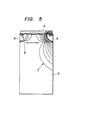
- Fig. 5 an example of the analytical result of the internal operation of a heterojunction semiconductor device according to the present invention is shown in Fig. 5.
- the current profile 8 is limited to the vicinity of the interface, between the first and second semiconductor layers 2, 3 and also a potential profile (denoted by contour lines) demonstrates a pinning effect on the drain side.
- the other reference numerals in Fig. 5 correspond to the same parts as those in Fig. 4.
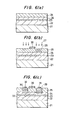
- Figs. 6(a) - 6(c) show the principal steps in the manufacture of such an FET.
- a GaAs layer 22 which is not intentionally doped with any impurity is grown on a semi-insulating GaAs substrate 21 to a thickness of about 1 ⁇ m (usually set at approximately 5000 R - 1.5 ⁇ m) at a substrate temperature of 580 0 C by employing the well-known method of molecular beam epitaxy.
- a GaAs layer 23 which contains a p-type dopant in GaAs, such as Zn, with a density of about 2 x 10 18 cm -3 (usually, 1 x 10 17 - 1 x 10 20 cm- 3 ) is grown to about 20 ⁇ (usually, 10 ⁇ - 500 ⁇ ) thereby to form a shielding region, and a GaAs layer 24 which is not intentionally doped with any impurity is grown to about 300 R (this value is set at a suitable value between 50 ⁇ and 2000 ⁇ , depending upon the characteristics of the device required), in succession by the use of molecular beam epitaxy.
- a GaAs layer 23 which contains a p-type dopant in GaAs, such as Zn, with a density of about 2 x 10 18 cm -3 (usually, 1 x 10 17 - 1 x 10 20 cm- 3 ) is grown to about 20 ⁇ (usually, 10 ⁇ - 500 ⁇ ) thereby to form a shielding region, and a
- the impurity- containing GaAs layer 23 may be a multilayer structure which consists of an n-type or p-type layer and a GaAs layer not doped with any impurity. Also, the layer 23 containing a p-type impurity may be replaced with a layer of a semiconductor having a greater band gap than GaAs, for example, with Al 0.3 Ga 0.7 As layer doped with no impurity.
- a GaAs layer which is not intentionally doped with any impurity and which is, for example, 500 R thick may be grown and a GaAs layer which contains an n-type dopant at a density of 5 x 10 17 cm and which is 20 ⁇ thick (usually, 10 - 500 R thick) may thereafter be grown by molecular beam epitaxy, in addition to the aforementioned p-type layer.
- This layer performs the role of the GaAs layer 23, i.e. forms a shielding region.
- Fig. 6(a) shows this state.
- a metal for example titanium (Ti) or tungsten (W) forming a gate electrode 26, is deposited on the above epitaxy layer of the multilayer structure to a thickness of about 2 ⁇ m, whereupon using the metal electrode 26 as a mask for ion implantation (self-alignment), Si ions 27 are implanted at a do se of 2 x 10 13 cm -2 by an acceleration voltage of 70 keV.
- Annealing is performed at 750 °C for 30 minutes in order to remove lattice defects generated by the ion implantation and to activate the ions.
- the resulting impurity regions 28 are shown in Fig. 6(b). Annealing at a high temperature of 850 °C enhances the activation rate of the ions.
- the annealing is preferably conducted at the temperature mentioned previously.
- Ge, Sn, Te, Se, S or the like may as the donor impurity be employed, as an alternative to Si.
- the impurity concentration of approximately 10 13 - 10 14 cm -3 to be ion-implanted is set, depending upon the extent to which carriers are to be generated, i.e. the required characteristics of the device.
- the energy of ion implantation differs depending upon the element to be implanted, but is normally set in a range of approximately 50 to 200 keV.
- source 29 and drain 30 electrode regions 30 are formed in continuation to the ion-implanted layers by the conventional alloying, and electrodes 31, 32 of metal aluminium are formed on the source 29 and drain regions respectively. Then, the field effect transistor is completed.
- the carriers 33 induced at the interface are shown in Fig. 6(c).
- the source and drain regions 29, 30 are formed so that, for example, an Au-Ge alloy (2000 R), Ni (100 ⁇ ) and an Au-Ge alloy (3000 ⁇ ) are stacked on predetermined parts and are heated at 400 °C in H 2 for about 5 minutes.
- an Au-Ge alloy 2000 R
- Ni 100 ⁇
- an Au-Ge alloy 3000 ⁇
- a transistor thus fabricated may have a mobility about 1.5 times and a transconductance about 3 times higher than those of prior-art heterojunction field effect transistors fabricated by doping AlGaAs with a donor at a density of about 2 x 10 18 cm -3 .
- the transistor fabrication efficiency it is possible to increase the transistor fabrication efficiency if a thin layer of GaAs, which is chemically more stable than AlGaAs, is grown on AlGaAs.
- the thickness of the layer is desirably approximately 300 ⁇ - 2000
- a GaAs layer 22 which is not intentionally doped with any impurity and which is about 1 ⁇ m thick is grown on a semi-insulating GaAs substrate 21 at a substrate temperature of 580 °C by molecular beam epitaxy, whereupon a GaAs layer 23 which contains Zn at a density of 10 19 cm -3 and which is about 20 R thick, and a GaAs layer 24 which is not intentionally doped with any impurity and which is about 500 R thick are successively grown using molecular beam epitaxy.
- a GaAlAs layer 25 which is not intentionally doped is grown to about 1200 R (Fig. 7(a)).
- the region to form the depletion-mode transistor is implanted with Si ions 26 at a density of 2 x 10 13 cm -3 and an energy of 70 keV (Fig. 7(b)).
- Gate electrodes 27 are then formed, whereupon using those electrodes 27 as a mask, regions 28 to form the source and drain electrodes of both transistors are subjected to a second ion implantation under the same conditions as in Embodiment 1, and the impurity is activated by similar annealing.
- the enhancement-mode and depletion-mode transistors can be fabricated simultaneously (Fig. 7(c)).
- the impurity concentration to be ion-implanted is set to be approximately 10 13 to 10 14 cm -3 , depending upon the extent to which carriers are to be induced, i.e. the required characteristics of the device.
- the energy of the ion implantation differs depending upon the element to be implanted, but is normally set in a range of approximately 50 to 200 keV.
- the source and drain regions are formed such that, for example, an A u-Ge alloy (2000 ⁇ ), N i (100 ⁇ ) and an Au-Ge alloy (3000 ⁇ ) are stacked on predetermined parts and are heated at 400 °C in H 2 for about 5 minutes (Fig. 7(d)).
Landscapes
- Junction Field-Effect Transistors (AREA)
- Insulated Gate Type Field-Effect Transistor (AREA)
Applications Claiming Priority (2)
| Application Number | Priority Date | Filing Date | Title |
|---|---|---|---|
| JP80895/83 | 1983-05-11 | ||
| JP58080895A JPS59207667A (ja) | 1983-05-11 | 1983-05-11 | 半導体装置 |
Publications (3)
| Publication Number | Publication Date |
|---|---|
| EP0130676A2 true EP0130676A2 (fr) | 1985-01-09 |
| EP0130676A3 EP0130676A3 (en) | 1986-08-13 |
| EP0130676B1 EP0130676B1 (fr) | 1990-08-16 |
Family
ID=13731094
Family Applications (1)
| Application Number | Title | Priority Date | Filing Date |
|---|---|---|---|
| EP84303165A Expired EP0130676B1 (fr) | 1983-05-11 | 1984-05-10 | Dispositif semi-conducteur ayant une hétéro-jonction |
Country Status (6)
| Country | Link |
|---|---|
| US (1) | US4605945A (fr) |
| EP (1) | EP0130676B1 (fr) |
| JP (1) | JPS59207667A (fr) |
| KR (1) | KR920003799B1 (fr) |
| CA (1) | CA1208807A (fr) |
| DE (1) | DE3482979D1 (fr) |
Cited By (1)
| Publication number | Priority date | Publication date | Assignee | Title |
|---|---|---|---|---|
| EP0415660A3 (en) * | 1989-08-28 | 1991-06-12 | Motorola Inc. | Fet having a high trap concentration interface layer and method of fabrication |
Families Citing this family (15)
| Publication number | Priority date | Publication date | Assignee | Title |
|---|---|---|---|---|
| JPH0793428B2 (ja) * | 1984-10-03 | 1995-10-09 | 株式会社日立製作所 | 半導体装置及びその製造方法 |
| JPH088350B2 (ja) * | 1985-04-08 | 1996-01-29 | 日本電気株式会社 | 半導体装置 |
| US5132752A (en) * | 1985-05-22 | 1992-07-21 | Hitachi, Ltd. | Field effect transistor |
| EP0214047B1 (fr) * | 1985-08-20 | 1993-12-22 | Fujitsu Limited | Transistor à effet de champ |
| USH411H (en) | 1985-08-28 | 1988-01-05 | United States Of America | Quasi-accumulation mode FET |
| JPH0824131B2 (ja) * | 1985-10-07 | 1996-03-06 | 株式会社日立製作所 | 電界効果トランジスタ |
| JPH084138B2 (ja) * | 1986-05-23 | 1996-01-17 | 日本電気株式会社 | 半導体装置 |
| US5214298A (en) * | 1986-09-30 | 1993-05-25 | Texas Instruments Incorporated | Complementary heterostructure field effect transistors |
| JPH0797636B2 (ja) * | 1986-09-30 | 1995-10-18 | 株式会社東芝 | ヘテロ接合電界効果トランジスタ |
| US4965645A (en) * | 1987-03-20 | 1990-10-23 | International Business Machines Corp. | Saturable charge FET |
| JPH01132170A (ja) * | 1987-11-18 | 1989-05-24 | Toshiba Corp | 電界効果トランジスタ |
| EP0323249B1 (fr) * | 1987-12-29 | 1993-11-03 | Nec Corporation | Structure cristalline à semi-conducteur et son procédé de fabrication |
| DE68928395T2 (de) * | 1988-06-28 | 1998-05-14 | Nippon Electric Co | Halbleitervorrichtung mit Verbindungshalbleiterfet mit E/D-Struktur mit hoher Geräuschmarge |
| US4962050A (en) * | 1988-12-06 | 1990-10-09 | Itt Corporation | GaAs FET manufacturing process employing channel confining layers |
| US5276340A (en) * | 1989-11-21 | 1994-01-04 | Fujitsu Limited | Semiconductor integrated circuit having a reduced side gate effect |
Family Cites Families (3)
| Publication number | Priority date | Publication date | Assignee | Title |
|---|---|---|---|---|
| CA1145482A (fr) * | 1979-12-28 | 1983-04-26 | Takashi Mimura | Dispositif a semiconducteur a heterojonction unique a grande mobilite electronique |
| DE3279663D1 (en) * | 1981-06-17 | 1989-06-01 | Hitachi Ltd | Heterojunction semiconductor device |
| JPS58143573A (ja) * | 1982-02-22 | 1983-08-26 | Nippon Telegr & Teleph Corp <Ntt> | 電界効果トランジスタ |
-
1983
- 1983-05-11 JP JP58080895A patent/JPS59207667A/ja active Pending
-
1984
- 1984-05-10 EP EP84303165A patent/EP0130676B1/fr not_active Expired
- 1984-05-10 KR KR1019840002515A patent/KR920003799B1/ko not_active Expired
- 1984-05-10 DE DE8484303165T patent/DE3482979D1/de not_active Expired - Lifetime
- 1984-05-11 CA CA000454153A patent/CA1208807A/fr not_active Expired
- 1984-05-11 US US06/609,446 patent/US4605945A/en not_active Expired - Lifetime
Cited By (1)
| Publication number | Priority date | Publication date | Assignee | Title |
|---|---|---|---|---|
| EP0415660A3 (en) * | 1989-08-28 | 1991-06-12 | Motorola Inc. | Fet having a high trap concentration interface layer and method of fabrication |
Also Published As
| Publication number | Publication date |
|---|---|
| DE3482979D1 (de) | 1990-09-20 |
| US4605945A (en) | 1986-08-12 |
| KR840009183A (ko) | 1984-12-24 |
| EP0130676B1 (fr) | 1990-08-16 |
| JPS59207667A (ja) | 1984-11-24 |
| KR920003799B1 (ko) | 1992-05-14 |
| CA1208807A (fr) | 1986-07-29 |
| EP0130676A3 (en) | 1986-08-13 |
Similar Documents
| Publication | Publication Date | Title |
|---|---|---|
| US5060031A (en) | Complementary heterojunction field effect transistor with an anisotype N+ ga-channel devices | |
| EP0130676B1 (fr) | Dispositif semi-conducteur ayant une hétéro-jonction | |
| EP0114962A2 (fr) | Transistor à effet de champ à double hétérojonction | |
| EP0206274A1 (fr) | Structure IC complémentaire à haute transconductance | |
| EP0051271B1 (fr) | Dispositif semiconducteur à hétérojonctions | |
| US4559547A (en) | Semiconductor device | |
| US4673959A (en) | Heterojunction FET with doubly-doped channel | |
| US5493136A (en) | Field effect transistor and method of manufacturing the same | |
| US5900641A (en) | Field effect semiconductor device having a reduced leakage current | |
| US5107314A (en) | Gallium antimonide field-effect transistor | |
| EP0131111B1 (fr) | Dispositif semi-conducteur ayant une hétéro-jonction | |
| JP3054216B2 (ja) | 半導体装置 | |
| US6015981A (en) | Heterostructure field-effect transistors (HFETs') with high modulation effectivity | |
| JP3653652B2 (ja) | 半導体装置 | |
| JP3053862B2 (ja) | 半導体装置 | |
| JP3304343B2 (ja) | 電界効果トランジスタ | |
| JPS60136380A (ja) | 半導体装置 | |
| EP0613191A2 (fr) | Structure de canal pour transistor à effet de champ | |
| JPH0513462A (ja) | 化合物半導体構造 | |
| KR960015325B1 (ko) | 쌍극자 전위 장벽을 갖는 전계효과 트랜지스터 | |
| JPH0864616A (ja) | 化合物半導体装置 | |
| JPH06295926A (ja) | 電界効果トランジスタを含む半導体装置 | |
| JPS6251268A (ja) | 半導体装置 | |
| JPH025437A (ja) | 電界効果トランジスタ及びその製造方法 | |
| JPH01268070A (ja) | ヘテロ接合型電界効果トランジスタ |
Legal Events
| Date | Code | Title | Description |
|---|---|---|---|
| PUAI | Public reference made under article 153(3) epc to a published international application that has entered the european phase |
Free format text: ORIGINAL CODE: 0009012 |
|
| 17P | Request for examination filed |
Effective date: 19840629 |
|
| AK | Designated contracting states |
Designated state(s): DE FR GB NL |
|
| PUAL | Search report despatched |
Free format text: ORIGINAL CODE: 0009013 |
|
| AK | Designated contracting states |
Kind code of ref document: A3 Designated state(s): DE FR GB NL |
|
| 17Q | First examination report despatched |
Effective date: 19890126 |
|
| GRAA | (expected) grant |
Free format text: ORIGINAL CODE: 0009210 |
|
| AK | Designated contracting states |
Kind code of ref document: B1 Designated state(s): DE FR |
|
| REF | Corresponds to: |
Ref document number: 3482979 Country of ref document: DE Date of ref document: 19900920 |
|
| ET | Fr: translation filed | ||
| PLBE | No opposition filed within time limit |
Free format text: ORIGINAL CODE: 0009261 |
|
| STAA | Information on the status of an ep patent application or granted ep patent |
Free format text: STATUS: NO OPPOSITION FILED WITHIN TIME LIMIT |
|
| 26N | No opposition filed | ||
| PGFP | Annual fee paid to national office [announced via postgrant information from national office to epo] |
Ref country code: FR Payment date: 20010516 Year of fee payment: 18 |
|
| PGFP | Annual fee paid to national office [announced via postgrant information from national office to epo] |
Ref country code: DE Payment date: 20010723 Year of fee payment: 18 |
|
| PG25 | Lapsed in a contracting state [announced via postgrant information from national office to epo] |
Ref country code: DE Free format text: LAPSE BECAUSE OF NON-PAYMENT OF DUE FEES Effective date: 20021203 |
|
| PG25 | Lapsed in a contracting state [announced via postgrant information from national office to epo] |
Ref country code: FR Free format text: LAPSE BECAUSE OF NON-PAYMENT OF DUE FEES Effective date: 20030131 |
|
| REG | Reference to a national code |
Ref country code: FR Ref legal event code: ST |