EP0133667A2 - Elektrisch löschbarer programmierbarer Nurlesespeicher hoher Dichte mit hohem Kopplungsverhältnis - Google Patents
Elektrisch löschbarer programmierbarer Nurlesespeicher hoher Dichte mit hohem Kopplungsverhältnis Download PDFInfo
- Publication number
- EP0133667A2 EP0133667A2 EP84108811A EP84108811A EP0133667A2 EP 0133667 A2 EP0133667 A2 EP 0133667A2 EP 84108811 A EP84108811 A EP 84108811A EP 84108811 A EP84108811 A EP 84108811A EP 0133667 A2 EP0133667 A2 EP 0133667A2
- Authority
- EP
- European Patent Office
- Prior art keywords
- region
- programmable read
- erasable programmable
- electrically erasable
- floating gate
- Prior art date
- Legal status (The legal status is an assumption and is not a legal conclusion. Google has not performed a legal analysis and makes no representation as to the accuracy of the status listed.)
- Withdrawn
Links
Images


Classifications
-
- H—ELECTRICITY
- H10—SEMICONDUCTOR DEVICES; ELECTRIC SOLID-STATE DEVICES NOT OTHERWISE PROVIDED FOR
- H10D—INORGANIC ELECTRIC SEMICONDUCTOR DEVICES
- H10D30/00—Field-effect transistors [FET]
- H10D30/60—Insulated-gate field-effect transistors [IGFET]
- H10D30/68—Floating-gate IGFETs
- H10D30/681—Floating-gate IGFETs having only two programming levels
- H10D30/683—Floating-gate IGFETs having only two programming levels programmed by tunnelling of carriers, e.g. Fowler-Nordheim tunnelling
Definitions
- This invention relates to semiconductor circuits and structures and in particular to electrically erasable programmable read-only memories (EEPROMs).
- EEPROMs electrically erasable programmable read-only memories
- ROMs Read-only memories
- EPROMs Erasable PROMs
- EPROMs when erased, lose all bits of information stored therein, and this is often referred as "bulk erasure".
- the most recent generation of memories is the electrically erasable programmable read-only memories (EEPROMs), which allow contents of a programmed EEPROM to be electrically erased, thereby allowing reprogramming. Because the entire circuit is not exposed to ultraviolet light in order to cause erasure of information stored therein, if properly designed, an EEPROM may 'allow erasure of a single word, or even a single bit, while retaining all other programmed information unchanged.
- EEPROMs electrically erasable programmable read-only memories
- a typical prior art EEPROM is described by Johnson, et al., in an article entitled "16-K EE-PROM Relies On Tunneling For Byte-Erasable Program Storage, Electronics, February 28, 1980, pages 113-117.
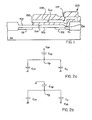
- a typical prior art EEPROM a memory cell is shown in Figure 1 and includes a transistor 100.having source 101 and drain 102 formed in a silicon substrate 99 and having a channel region 103 formed therebetween.
- a layer of gate insulation 104 electrically insulates a floating gate 105 formed above the channel 103, and extending over the drain 102.
- a very thin tunnel oxide region 106 electrically insulates a small portion of the floating gate 105 from the drain 102.
- This prior art structure further includes a control gate 108, and a layer of insulation 107 formed between the floating gate 105 and the control gate 108.
- C ch is the capacitance formed between floating gate 105 and channel region 103
- capacitance Cpp is the capacitance formed between control gate 108 and floating gate 105
- capacitance C t is the capacitance formed between floating gate 105 and drain 102.
- This injection of electrons on the floating gate is accomplished for example, by Fowler-Nordheim tunneling.
- One technique for this electron tunneling is to place a high voltage (typically 10 to 20 volts) on the control gate 108, and grounding the drain 102, source 101 and substrate 99. This causes electrons to tunnel from the drain region 102 through the tunneling oxide 106 to the floating gate 105.
- Vt control gate threshold voltage
- the floating gate 105 In order to erase a memory cell or, in other words, to change the state of a memory cell from a logical zero to a logical one, the floating gate 105 is discharged. This is accomplished, for example, by placing the control gate 108 at ground, a high positive voltage on the drain 102, (typically +20 volts) disconnecting the source 101 (i.e., the source is "floating"), and connecting the substrate 99 to ground. This causes electrons to flow from the floating gate 105 through the tunelling oxide 106 to the drain 102, thereby discharging the floating gate 105, decreasing the control gate threshold voltage, and storing a logical zero in the memory cell 100.
- a high positive voltage on the drain 102 typically +20 volts
- FIG. 2a Shown in Figure 2a is the connection of the various capacitances of cell 100 of Figure 1 during the programming of cell 100 to store logical zero.
- the control gate 108 is connected to a high programming voltage V , and the drain 102, source 101 and substrate 99 (and thus the channel region 103) are grounded.
- V pp the voltage V between the floating gate 105 and the drain 102 may be expressed as a fraction of the programming voltage V pp as follows: or '
- the various capacitances cell 100 may be calculated utilizing the following equation:
- the speed of charging the floating gate (i.e., programming the cell) and discharging the floating gate (i.e., erasing the cell) is determined by the magnitude of the electric field across the tunneling dielectric 106. This in turn is dependent on the magnitude of the voltgage V pp which is applied between the control gate 108 and the tunneling region (i.e., drain 102) within the substrate beneath the tunneling dielectric 106, as well as the coupling ratio of the cell.
- the coupling ratio defines what portion of the applied voltage V pp appears across the tunneling dielectric 106 between the floating gate 105 and the tunneling region (i.e., drain) 102.
- the value of C should be made as small as possible, and the value of capacitances C ch and C pp should be as large as possible.
- capacitance C t There are practical limits to the minimum plate size of capacitance C t; using technology capable of producing.3 micron.line widths, a C t plate size of approximately 2.25 x 1.0 microns is perhaps the minimum possible.
- the thickness of tunneling dielectric 106 must be made sufficiently small to allow efficient tunneling to occur between floating gate 105 and source 102.
- the capacitances C ch and Cpp can be increased without limit thus aiding the efficiency of the cell, however maintaining a small cell size is critical. Thus, there is a tradeoff to be made between reduced cell size versus increased programming and erasing efficiencies. Furthermore, increasing the programming and erasing voltage Vpp will increase the speed of programming and erasing the EEPROM cell. However, it is also highly desirable to minimize the programmable voltage V pp , thereby to prevent circuit failure due to undesired voltage breakdowns, as well as to allow the EEPROM cells to be used in circuits which do not need to provide a rather high voltage as V pp
- U.S. Patent No. 4,361,847 issued November 30, 1982, to Harari discloses a unique electrically erasable, programmable read-only memory cell wherein, in contrast to other prior art structures, the tunneling dielectric is formed over a portion of the channel region and the floating gate extends over the drain diffusion and only a portion of the channel region. Harari's structure alo requires that the capacitance between the source and the floating gate be held to a minimum.
- Other prior art EEPROM devices are described in U. S. Patents No. 4,342,099; 4,267,632; and 4,115,914 which, together with the previously.mentioned U.S. Patent No. 4,361,847, are hereby incorporated by reference.
- the EEPROM cell includes not only a source, a channel, and a drain region located within a semiconductor substrate, but also a separate and distinct programming diffusion.
- the tunneling oxide rather than being formed over the drain region, is located over the tunneling region, and the floating gate extends not only over the source, the channel and the drain, but over the tunneling region as well.
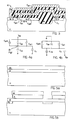
- Figure 3 is a cross-sectional view of one embodiment of an EEPROM cell constructed in accordance with this invention.
- the cell of Figure 3 will be described as being fabricated in a P type silicon substrate, having N type diffused regions formed therein, and utilizing polycrystalline silicon interconnects and gates.
- other embodiments of my invention utilize different conductivity types and interconnects made of materials other than polycrystalline silicon, such as aluminum, alloys of aluminum, refractory metals, and alloys of refractory metals.
- N-type drain region 18-3 Within P-type substrate 11 is formed N-type drain region 18-3, N-type source region 18-2, and a unique N-type programming region 18-1 which is separated from source region 18-2 by thick field oxide 16.
- a channel region 18-4 is formed within substrate 11 between drain region 18-3 and source region 18-2.
- a gate dielectric (e.g., oxide) 19 is formed on the surface of the substrate 11 over drain region 18-3, source region 18-2, the channel region 18-4, and a portion of programming region 18-1.
- thin tunneling dielectric 20 Above the remaining portion of programming region 18-1 is formed thin tunneling dielectric 20, which allows electrons to flow (by tunneling) between the floating gate 21 and programming region 18-1 during programming and erasure of cell 10.
- Floating gate 21 is formed above drain 18-3, channel 18-4, source 18-2, and programming region 18-1. Formed on the sides and top of floating gate 21 is dielectric layer 22 (such as oxide), above which is formed control gate 23, which is connected to drain 18-3, as shown. If desired, the floating gate 21 need not be electrically connected to drain 18-3 if other means of applying to drain 18-3 the voltages necessary to program and erase the cell are provided. Those of ordinary skill in the art will appreciate that gate oxide 19 need not be formed over any portion of tunneling region 18-1; the formation of thin tunneling oxide 20 and the insulation of floating gate 21 from programming region 18-1 is of importance.
- tunneling dielectric may be formed of, for example, silicon nitride, silicon dioxide, or a "sandwich" formed of silicon dioxide and silicon nitride.
- control gate 23 need not be formed, and the data (i.e., logical one or zero) stored in the memory cell is determined by whether current flows between the source 18-2 and the drain 18-3 as a result of the voltages applied thereto as well as the charge stored on floating gate 21.
- a capacitance Cp rl is formed between floating gate 21 and drain 18-3, a capacitance C ch is formed between floating gate 21 and channel 18-4, a capacitance Cp r2 is formed between floating gate 21 and source 18-2, a capacitance C t is formed between floating gate 21 and programming region 18-1, and a capacitance C is formed between polycrystalline silicon control gate 23 and polycrystalline silicon floating gate 21.
- substrate 11 and tunneling region 18-1 are connected to ground, and control gate 23 (and thus drain 18-3) and source 18-2 are connected to a highly positive programming voltage V pp (typically 20 volts).
- V pp typically 20 volts
- This negative potential on floating gate 21 causes the control gate threshold voltage to be increased, thus indicating that cell 10 stores a logical zero.
- electrons are removed from floating gate 21 in order to lower the control gate threshold voltage and thus store a logical one in cell 10.
- Vpp typically 20 volts
- FIG. 4a Shown in Figure 4a is the connection of the various capacitances of cell 10 of Figure 3 during the programming of cell 10 to store a logical zero.
- the substrate 11 and thus the channel region 18-4) and tunneling area 18-1 are connected to ground, and control gate 23, drain 18-3, and source 18-2 connected to a positive programming voltage V .
- the voltage V F between floating gate 21 and tunneling region 18-1 may be expressed as a fraction of the programming voltage V pp as follows: or
- the programming efficiency a of an EEPROM cell construction in accordance with my invention is improved as compared with that of a prior art EEPROM having similar plate dimensions and cell size.
- the EEPROM cell constructed in accordance with my invention included capacitances C pp1 and C pp2 as indicated by the above equations, the erasing efficiency of an EEPROM cell construction in accordance with my invention is improved as compared with that of a prior art EEPROM having similar plate dimensions and cell size.
- the programming efficiency ⁇ (equation (10)) is approximately 90% and the erasing efficiency p (equation (13)) is approximately 95%.
- the test structure referred to in Table 2 is slightly larger than the prior art EEPROM cell referred to in Table 1.
- the principles of this invention can easily be applied by one of ordinary skill in the art to fabricate EEPROM cells having the same or smaller cell size than prior art EEPROM cells, while still providing the increased programming and erasing efficiencies made possible by my invention.
- FIG. 5a One process for fabricating a device in accordance with one embodiment of my invention is depicted in the cross-sectional views of Figures 5a through 5h.
- a P-type substrate 11 having crystal orientation ⁇ 100> and having a resistivity within the range of approximately 30 to 66 ohm-cm is used.
- a layer of base oxidation 12 is formed to a thickness within the range of approximately 700 to 800A by, for example, oxidation in dry oxygen plus approximately 3% HCL for approximately 55 minutes at approximately 1,000°C.
- suitable "ramp up” and “ramp down” temperatures in suitable atmospheres are utilized to prevent excessive thermal shock to the wafer undergoing this base oxidation step.
- a layer of silicon nitride 13 is formed to a thickness within the ° range of approximately 1400 to 1600A by, for example, low pressure chemical vapor deposition (LPCVD) as described, for example, in an article by Rosler entitled “Low Pressure CVD Production Processes For Poly, Nitride, and Oxide", Solid-State Technology, April 1977, pages 63-70, which is hereby incorporated by reference.
- LPCVD low pressure chemical vapor deposition
- a layer of photoresist 14 is formed in a well known manner and patterned utilizing suitable photolithographic techniques well known to those of ordinary skill in the art in order to define those regions in which field oxide is to be formed.
- Nitride layer 13 is then patterned, for example, utilizing a CF 4 plasma, in order to expose those portions of base oxide 12 where field oxide is to be formed.
- a field implant is performed in order to increase the field inversion voltage. This is performed, for example, by the ion implantation of boron to a dosage of approximately 3.0 X 10 13 ions/cm 2 at an energy level of approximately 70 KEV.
- the implanted boron is indicated by the dashed lines labeled 15 in Figure 5b.
- photoresist 14 is then removed utilizing suitable well known techniques.
- the portions of base oxide 12 exposed by nitride layer 13 is then removed, for example, by etching with buffered HF.
- field oxide 16 is then grown in those regions of the substrate 11 exposed by nitride layer 13 to a thickness within the range of approximately 12,000 to 14,OOOA by, for example, oxidation in wet 0 2 at approximately 900°C for approximately 840 minutes.
- the remaining portions of nitride layer 13 are then removed, for example, by etching with a CF 4 plasma, thereby providing the structure shown in Figure 5c.
- a layer of photoresist 17 is formed and patterned, utilizing suitable well known photolithographic techniques, in order to protect the base oxide 12 overlying the channel regions of the to be formed EEPROM cell. Undesired portions of base oxide are then removed, for example, by etching with buffered HF. Source and drain regions 18-2 and 18-3, respectively, are then formed, for example by the implantation of arsenic ions to a dosage of 8.0 x 10 15 ions/cm 2 at an energy level of approximately 50 KEV.
- Photoresist 17 is then removed, and the remaining portions of base oxide 12 are removed, for example, using buffered HF.
- Gate oxide 19 is then formed as shown in Figure 5f, for example, by oxidation in dry oxygen containing approximately 3% HCL for approximately 55 minutes at approximately 1000°C. This results in gate oxide 19 having a thickness within the range of approximately 700 o to 800 A.
- a layer of photoresist (not shown) is then applied to the surface of the wafer and patterned to expose that portion of the wafer upon which is to be formed the tunneling region 18-1 (Fig. 3).
- Gate oxide 19 is then removed in this area, for example, by etching with buffered HF.
- Tunneling region 18-1 is then formed, for example, by the implantation of arsenic to a dosage of approximately 1 x 10 14 ions/cm 2 at energy of approximately 100 KEV.
- the photoresist is then removed, and the tunneling oxide 20 is 0 formed, for example, to a thickness of approximately 100A.
- Tunneling oxide 20 is formed, for example, by thermal oxidation by transferring the wafer from an ambient atmosphere to a nitrogen atmosphere containing approximately 1% oxygen at a temperature of approximate 900°C during a 10 minutes "push" cycle, holding the wafer in the 1% oxygen/99% nitrogen atmosphere at approximately 900°C, for approximately 10 minutes, changing the atmosphere to pure oxygen at approximately 900°C for a period of approximately five minutes, changing the atmosphere to nitrogen containing approximately 9% HCL at approximately 900°C for approximately 10 minutes, changing the atmosphere to pure oxygen at approximately 900°C for approximately 10 minutes, changing the atmosphere to pure nitrogen at approximately 900°C for approximately 10 minutes, and removing the wafer from the pure nitrogen atmosphere to an ambient atmosphere during a 10 minute "pull" cycle.
- a layer of polycrystalline silicon 21, which will serve as the floating gate of the EEPROM device, is formed to a thickness within the range ° of approximately 3900 to 4600A using, for example, low pressure chemical vapor deposition.
- a layer of photoresist (not shown) is then formed in order to expose those portions of polycrystalline silicon layer 21 which are to be removed and to protect those portions of polycrystalline silicon layer 21 which are to remain to form floating gate 21.
- Exposed portions of polycrystalline silicon layer 21 are then removed, for example, using a CF 4 plasma.
- the photoresist is then removed, and the polycrystalline silicon is then doped, for example, with POCl 3 , in order to have a V/I characteristic within the range of approximately 2.5 to 3.5.
- Oxide layer 22, shown in Figure 5g is then formed to a thickness within the range of approxi-0 mately 700 to 800A by, for example, oxidizing polycrystalline silicon layer 21 for approximately 30 minutes in oxygen at 1100°C.
- a layer of polycrystalline silicon 22 is then formed to a thickness of 0 approximately 3800 to 4500A by, for example, low pressure chemical vapor deposition.
- Polycrystalline silicon layer 22 is then doped with, for example, POC1 3 , to have a V/I characteristic within the range of approximately 2.5 to 3.5.
- Polycrystalline silicon layer 22 which will serve as the control gate of the EEPROM cells, is then defined utilizing well known photolithographic techniques and patterned, for example, utilizing a CF 4 plasma.
- additional processing steps are used to form additional insulation layers on the surface of the device, and if desired, additional layers of electrical interconnects, for example, aluminum. These final processing steps are well known to those of ordinary skill in the art and thus will not be described here.
Landscapes
- Non-Volatile Memory (AREA)
Applications Claiming Priority (2)
| Application Number | Priority Date | Filing Date | Title |
|---|---|---|---|
| US52289083A | 1983-08-12 | 1983-08-12 | |
| US522890 | 1995-09-01 |
Publications (2)
| Publication Number | Publication Date |
|---|---|
| EP0133667A2 true EP0133667A2 (de) | 1985-03-06 |
| EP0133667A3 EP0133667A3 (en) | 1987-08-26 |
Family
ID=24082795
Family Applications (1)
| Application Number | Title | Priority Date | Filing Date |
|---|---|---|---|
| EP84108811A Withdrawn EP0133667A3 (en) | 1983-08-12 | 1984-07-25 | High coupling ratio dense electrically erasable programmable read-only memory |
Country Status (2)
| Country | Link |
|---|---|
| EP (1) | EP0133667A3 (de) |
| JP (1) | JPS6055670A (de) |
Cited By (5)
| Publication number | Priority date | Publication date | Assignee | Title |
|---|---|---|---|---|
| EP0231507A3 (en) * | 1986-01-03 | 1988-04-20 | Sierra Semiconductor Corporation | An electrically alterable non-volatile memory device |
| EP0268315A3 (en) * | 1986-11-18 | 1988-12-14 | Sgs-Thomson Microelectronics S.P.A. | Eeprom memory cell with a single polysilicon level and a tunnel oxide zone |
| EP0389693A1 (de) * | 1989-03-31 | 1990-10-03 | Koninklijke Philips Electronics N.V. | EPROM, der eine mehrfache Verwendung der Bitleitungskontakte ermöglicht |
| US5309009A (en) * | 1992-09-14 | 1994-05-03 | Chao Robert L | Integrated electrically adjustable analog transistor device |
| US5656838A (en) * | 1994-04-19 | 1997-08-12 | Nec Corporation | Non-volatile semiconductor memory having programming region for injecting and ejecting carriers into and from floating gate |
Families Citing this family (1)
| Publication number | Priority date | Publication date | Assignee | Title |
|---|---|---|---|---|
| JP7372047B2 (ja) * | 2018-05-25 | 2023-10-31 | 旭化成エレクトロニクス株式会社 | 不揮発性記憶素子 |
Family Cites Families (4)
| Publication number | Priority date | Publication date | Assignee | Title |
|---|---|---|---|---|
| JPS58130571A (ja) * | 1982-01-29 | 1983-08-04 | Hitachi Ltd | 半導体装置 |
| US4558344A (en) * | 1982-01-29 | 1985-12-10 | Seeq Technology, Inc. | Electrically-programmable and electrically-erasable MOS memory device |
| GB2126788B (en) * | 1982-03-09 | 1985-06-19 | Rca Corp | An electrically alterable nonvolatile floating gate memory device |
| FR2562707A1 (fr) * | 1984-04-06 | 1985-10-11 | Efcis | Point-memoire electriquement effacable et reprogrammable, comportant une grille flottante au-dessus d'une grille de commande |
-
1984
- 1984-07-25 EP EP84108811A patent/EP0133667A3/en not_active Withdrawn
- 1984-07-30 JP JP59160171A patent/JPS6055670A/ja active Pending
Cited By (8)
| Publication number | Priority date | Publication date | Assignee | Title |
|---|---|---|---|---|
| EP0231507A3 (en) * | 1986-01-03 | 1988-04-20 | Sierra Semiconductor Corporation | An electrically alterable non-volatile memory device |
| EP0268315A3 (en) * | 1986-11-18 | 1988-12-14 | Sgs-Thomson Microelectronics S.P.A. | Eeprom memory cell with a single polysilicon level and a tunnel oxide zone |
| EP0389693A1 (de) * | 1989-03-31 | 1990-10-03 | Koninklijke Philips Electronics N.V. | EPROM, der eine mehrfache Verwendung der Bitleitungskontakte ermöglicht |
| US5017978A (en) * | 1989-03-31 | 1991-05-21 | U.S. Philips Corp. | EPROM having a reduced number of contacts |
| US5309009A (en) * | 1992-09-14 | 1994-05-03 | Chao Robert L | Integrated electrically adjustable analog transistor device |
| US5656838A (en) * | 1994-04-19 | 1997-08-12 | Nec Corporation | Non-volatile semiconductor memory having programming region for injecting and ejecting carriers into and from floating gate |
| US5801414A (en) * | 1994-04-19 | 1998-09-01 | Nec Corporation | Non-volatile semiconductor memory having programming region for injecting and ejecting carriers into and from a floating gate |
| EP0875943A3 (de) * | 1994-04-19 | 1998-12-09 | Nec Corporation | Nicht-flüchtiger Halbleiterspeicher mit Programmierbereichen durch Injektion und Ejektion von Ladungsträgern in und aus einer schwebenden Steuerelektrode |
Also Published As
| Publication number | Publication date |
|---|---|
| EP0133667A3 (en) | 1987-08-26 |
| JPS6055670A (ja) | 1985-03-30 |
Similar Documents
| Publication | Publication Date | Title |
|---|---|---|
| US4688078A (en) | Partially relaxable composite dielectric structure | |
| US5099297A (en) | EEPROM cell structure and architecture with programming and erase terminals shared between several cells | |
| JP3710082B2 (ja) | メモリ・トランジスタを作成する方法 | |
| US4274012A (en) | Substrate coupled floating gate memory cell | |
| US6458656B1 (en) | Process for creating a flash memory cell using a photoresist flow operation | |
| US5869369A (en) | Method of fabricating a flash memory | |
| EP0557581A2 (de) | Nichtflüchtige DRAM-Zelle | |
| US20040108537A1 (en) | Scalable nano-transistor and memory using back-side trapping | |
| US20020009852A1 (en) | Method of manufacturing semiconductor device | |
| EP0083387B1 (de) | Speicheranordnung | |
| EP0105802A2 (de) | Programmierbarer Nurlesespeicher | |
| US6232634B1 (en) | Non-volatile memory cell and method for manufacturing same | |
| US5583066A (en) | Method of fabricating nonvolatile semiconductor memory element having elevated source and drain regions | |
| US5504708A (en) | Flash EEPROM array with P-tank insulated from substrate by deep N-tank | |
| EP0177816B1 (de) | Nichtflüchtige dynamische Schreib-/Lesespeicher mit wahlfreiem Zugriff | |
| US5087583A (en) | Process for EEPROM cell structure and architecture with shared programming and erase terminals | |
| US5973355A (en) | Nonvolatile semiconductor memory device and manufacturing method of the same | |
| US5017980A (en) | Electrically-erasable, electrically-programmable read-only memory cell | |
| US5166904A (en) | EEPROM cell structure and architecture with increased capacitance and with programming and erase terminals shared between several cells | |
| US5332914A (en) | EEPROM cell structure and architecture with increased capacitance and with programming and erase terminals shared between several cells | |
| US5304505A (en) | Process for EEPROM cell structure and architecture with increased capacitance and with programming and erase terminals shared between several cells | |
| EP0133667A2 (de) | Elektrisch löschbarer programmierbarer Nurlesespeicher hoher Dichte mit hohem Kopplungsverhältnis | |
| US6117756A (en) | Method of forming high density and low power flash memories with a high capacitive-coupling ratio | |
| US6008087A (en) | Method to form high density NAND structure nonvolatile memories | |
| KR100872581B1 (ko) | 소스 및 채널 영역을 모두 이용한 플래시 메모리 셀 소거방식 |
Legal Events
| Date | Code | Title | Description |
|---|---|---|---|
| PUAI | Public reference made under article 153(3) epc to a published international application that has entered the european phase |
Free format text: ORIGINAL CODE: 0009012 |
|
| AK | Designated contracting states |
Designated state(s): AT DE FR GB IT NL SE |
|
| 17P | Request for examination filed |
Effective date: 19841227 |
|
| PUAL | Search report despatched |
Free format text: ORIGINAL CODE: 0009013 |
|
| AK | Designated contracting states |
Kind code of ref document: A3 Designated state(s): AT DE FR GB IT NL SE |
|
| STAA | Information on the status of an ep patent application or granted ep patent |
Free format text: STATUS: THE APPLICATION IS DEEMED TO BE WITHDRAWN |
|
| 18D | Application deemed to be withdrawn |
Effective date: 19880227 |
|
| RIN1 | Information on inventor provided before grant (corrected) |
Inventor name: MALTIEL, RON |