EP0139371A1 - Procédé pour fabriquer un circuit intégré de type MOS utilisant une méthode pour former des couches en siliciure de métaux réfractaires - Google Patents
Procédé pour fabriquer un circuit intégré de type MOS utilisant une méthode pour former des couches en siliciure de métaux réfractaires Download PDFInfo
- Publication number
- EP0139371A1 EP0139371A1 EP84305444A EP84305444A EP0139371A1 EP 0139371 A1 EP0139371 A1 EP 0139371A1 EP 84305444 A EP84305444 A EP 84305444A EP 84305444 A EP84305444 A EP 84305444A EP 0139371 A1 EP0139371 A1 EP 0139371A1
- Authority
- EP
- European Patent Office
- Prior art keywords
- layer
- refractory metal
- gate
- drain
- source
- Prior art date
- Legal status (The legal status is an assumption and is not a legal conclusion. Google has not performed a legal analysis and makes no representation as to the accuracy of the status listed.)
- Granted
Links
Images


Classifications
-
- H—ELECTRICITY
- H10—SEMICONDUCTOR DEVICES; ELECTRIC SOLID-STATE DEVICES NOT OTHERWISE PROVIDED FOR
- H10D—INORGANIC ELECTRIC SEMICONDUCTOR DEVICES
- H10D62/00—Semiconductor bodies, or regions thereof, of devices having potential barriers
- H10D62/80—Semiconductor bodies, or regions thereof, of devices having potential barriers characterised by the materials
- H10D62/83—Semiconductor bodies, or regions thereof, of devices having potential barriers characterised by the materials being Group IV materials, e.g. B-doped Si or undoped Ge
-
- H—ELECTRICITY
- H10—SEMICONDUCTOR DEVICES; ELECTRIC SOLID-STATE DEVICES NOT OTHERWISE PROVIDED FOR
- H10D—INORGANIC ELECTRIC SEMICONDUCTOR DEVICES
- H10D64/00—Electrodes of devices having potential barriers
- H10D64/60—Electrodes characterised by their materials
- H10D64/62—Electrodes ohmically coupled to a semiconductor
-
- H—ELECTRICITY
- H10—SEMICONDUCTOR DEVICES; ELECTRIC SOLID-STATE DEVICES NOT OTHERWISE PROVIDED FOR
- H10D—INORGANIC ELECTRIC SEMICONDUCTOR DEVICES
- H10D64/00—Electrodes of devices having potential barriers
- H10D64/60—Electrodes characterised by their materials
- H10D64/66—Electrodes having a conductor capacitively coupled to a semiconductor by an insulator, e.g. MIS electrodes
- H10D64/661—Electrodes having a conductor capacitively coupled to a semiconductor by an insulator, e.g. MIS electrodes the conductor comprising a layer of silicon contacting the insulator, e.g. polysilicon having vertical doping variation
- H10D64/662—Electrodes having a conductor capacitively coupled to a semiconductor by an insulator, e.g. MIS electrodes the conductor comprising a layer of silicon contacting the insulator, e.g. polysilicon having vertical doping variation the conductor further comprising additional layers, e.g. multiple silicon layers having different crystal structures
- H10D64/663—Electrodes having a conductor capacitively coupled to a semiconductor by an insulator, e.g. MIS electrodes the conductor comprising a layer of silicon contacting the insulator, e.g. polysilicon having vertical doping variation the conductor further comprising additional layers, e.g. multiple silicon layers having different crystal structures the additional layers comprising a silicide layer contacting the layer of silicon, e.g. polycide gates
-
- H—ELECTRICITY
- H10—SEMICONDUCTOR DEVICES; ELECTRIC SOLID-STATE DEVICES NOT OTHERWISE PROVIDED FOR
- H10D—INORGANIC ELECTRIC SEMICONDUCTOR DEVICES
- H10D84/00—Integrated devices formed in or on semiconductor substrates that comprise only semiconducting layers, e.g. on Si wafers or on GaAs-on-Si wafers
- H10D84/01—Manufacture or treatment
- H10D84/0123—Integrating together multiple components covered by H10D12/00 or H10D30/00, e.g. integrating multiple IGBTs
- H10D84/0126—Integrating together multiple components covered by H10D12/00 or H10D30/00, e.g. integrating multiple IGBTs the components including insulated gates, e.g. IGFETs
- H10D84/0165—Integrating together multiple components covered by H10D12/00 or H10D30/00, e.g. integrating multiple IGBTs the components including insulated gates, e.g. IGFETs the components including complementary IGFETs, e.g. CMOS devices
- H10D84/0172—Manufacturing their gate conductors
- H10D84/0174—Manufacturing their gate conductors the gate conductors being silicided
-
- H—ELECTRICITY
- H10—SEMICONDUCTOR DEVICES; ELECTRIC SOLID-STATE DEVICES NOT OTHERWISE PROVIDED FOR
- H10D—INORGANIC ELECTRIC SEMICONDUCTOR DEVICES
- H10D84/00—Integrated devices formed in or on semiconductor substrates that comprise only semiconducting layers, e.g. on Si wafers or on GaAs-on-Si wafers
- H10D84/01—Manufacture or treatment
- H10D84/02—Manufacture or treatment characterised by using material-based technologies
- H10D84/03—Manufacture or treatment characterised by using material-based technologies using Group IV technology, e.g. silicon technology or silicon-carbide [SiC] technology
- H10D84/038—Manufacture or treatment characterised by using material-based technologies using Group IV technology, e.g. silicon technology or silicon-carbide [SiC] technology using silicon technology, e.g. SiGe
-
- H—ELECTRICITY
- H10—SEMICONDUCTOR DEVICES; ELECTRIC SOLID-STATE DEVICES NOT OTHERWISE PROVIDED FOR
- H10P—GENERIC PROCESSES OR APPARATUS FOR THE MANUFACTURE OR TREATMENT OF DEVICES COVERED BY CLASS H10
- H10P30/00—Ion implantation into wafers, substrates or parts of devices
- H10P30/20—Ion implantation into wafers, substrates or parts of devices into semiconductor materials, e.g. for doping
- H10P30/22—Ion implantation into wafers, substrates or parts of devices into semiconductor materials, e.g. for doping using masks
-
- H—ELECTRICITY
- H10—SEMICONDUCTOR DEVICES; ELECTRIC SOLID-STATE DEVICES NOT OTHERWISE PROVIDED FOR
- H10W—GENERIC PACKAGES, INTERCONNECTIONS, CONNECTORS OR OTHER CONSTRUCTIONAL DETAILS OF DEVICES COVERED BY CLASS H10
- H10W10/00—Isolation regions in semiconductor bodies between components of integrated devices
- H10W10/01—Manufacture or treatment
- H10W10/011—Manufacture or treatment of isolation regions comprising dielectric materials
- H10W10/012—Manufacture or treatment of isolation regions comprising dielectric materials using local oxidation of silicon [LOCOS]
-
- H—ELECTRICITY
- H10—SEMICONDUCTOR DEVICES; ELECTRIC SOLID-STATE DEVICES NOT OTHERWISE PROVIDED FOR
- H10W—GENERIC PACKAGES, INTERCONNECTIONS, CONNECTORS OR OTHER CONSTRUCTIONAL DETAILS OF DEVICES COVERED BY CLASS H10
- H10W10/00—Isolation regions in semiconductor bodies between components of integrated devices
- H10W10/01—Manufacture or treatment
- H10W10/041—Manufacture or treatment of isolation regions comprising polycrystalline semiconductor materials
-
- H—ELECTRICITY
- H10—SEMICONDUCTOR DEVICES; ELECTRIC SOLID-STATE DEVICES NOT OTHERWISE PROVIDED FOR
- H10W—GENERIC PACKAGES, INTERCONNECTIONS, CONNECTORS OR OTHER CONSTRUCTIONAL DETAILS OF DEVICES COVERED BY CLASS H10
- H10W10/00—Isolation regions in semiconductor bodies between components of integrated devices
- H10W10/10—Isolation regions comprising dielectric materials
- H10W10/13—Isolation regions comprising dielectric materials formed using local oxidation of silicon [LOCOS], e.g. sealed interface localised oxidation [SILO] or side-wall mask isolation [SWAMI]
-
- H—ELECTRICITY
- H10—SEMICONDUCTOR DEVICES; ELECTRIC SOLID-STATE DEVICES NOT OTHERWISE PROVIDED FOR
- H10W—GENERIC PACKAGES, INTERCONNECTIONS, CONNECTORS OR OTHER CONSTRUCTIONAL DETAILS OF DEVICES COVERED BY CLASS H10
- H10W10/00—Isolation regions in semiconductor bodies between components of integrated devices
- H10W10/40—Isolation regions comprising polycrystalline semiconductor materials
Definitions
- Still another object of the invention is to provide such a method of manufacture in which the refractory metal silicide layer is formed by depositing two refractory metal layers including an inner layer of low resistance metal, such as titanium or tantalum, which forms the silicide and an outer layer of a non-oxidizing refractory metal, such as molybdenum, which prevents oxidation of the inner layer to enable the portions of the inner layer which do not form a silicide to be selectively removed by etching to leave self-aligned silicide areas on only the source, drain and gate elements of the transistor.
- an inner layer of low resistance metal such as titanium or tantalum
- a non-oxidizing refractory metal such as molybdenum
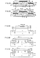
- An aluminum-silicon alloy contact region 66 is deposited through each contact opening 64 by sputtering to provide ohmic contacts with the source and drain regions 56 and 60 in the N well layer 30 and the source and drain regions 60 in the expitaxial layer region 12 to the left of the trench 20. Then the photoresist layer used to form the ohmic contact deposition region 66 is removed and the entire integrated circuit is again heated for annealing to insure that the ohmic contacts 66 form good electrical contact with the source and drain portions of the field effect transistors.
- the second nitride layer 102 is removed by reactive ion etching except for side wall portions 104 which are coated over the vertical side walls of the raised portion of epitaxial layer 12 covered by the oxide layer 100, and over the ends of the first nitride layer 94.
- the reactive ion etching step etches anisotropically in a downward vertical direction but not horizontally to any appreciable extent.
- the reactive ion etching solution may be made of CHF 3 + H 2 gas which removes silicon nitride but does not etch silicon.
Landscapes
- Metal-Oxide And Bipolar Metal-Oxide Semiconductor Integrated Circuits (AREA)
- Element Separation (AREA)
- Electrodes Of Semiconductors (AREA)
- Insulated Gate Type Field-Effect Transistor (AREA)
Applications Claiming Priority (2)
| Application Number | Priority Date | Filing Date | Title |
|---|---|---|---|
| US522885 | 1983-08-12 | ||
| US06/522,885 US4477310A (en) | 1983-08-12 | 1983-08-12 | Process for manufacturing MOS integrated circuit with improved method of forming refractory metal silicide areas |
Publications (2)
| Publication Number | Publication Date |
|---|---|
| EP0139371A1 true EP0139371A1 (fr) | 1985-05-02 |
| EP0139371B1 EP0139371B1 (fr) | 1988-07-20 |
Family
ID=24082771
Family Applications (1)
| Application Number | Title | Priority Date | Filing Date |
|---|---|---|---|
| EP84305444A Expired EP0139371B1 (fr) | 1983-08-12 | 1984-08-09 | Procédé pour fabriquer un circuit intégré de type MOS utilisant une méthode pour former des couches en siliciure de métaux réfractaires |
Country Status (4)
| Country | Link |
|---|---|
| US (1) | US4477310A (fr) |
| EP (1) | EP0139371B1 (fr) |
| JP (1) | JPS60149166A (fr) |
| DE (1) | DE3472860D1 (fr) |
Cited By (5)
| Publication number | Priority date | Publication date | Assignee | Title |
|---|---|---|---|---|
| FR2578097A1 (fr) * | 1985-02-26 | 1986-08-29 | Efcis | Procede de fabrication de circuits integres en technologie mos et cmos et structure cmos correspondante |
| GB2183907A (en) * | 1985-11-27 | 1987-06-10 | Raytheon Co | Reducing radiation effects on integrated circuits |
| US4936928A (en) * | 1985-11-27 | 1990-06-26 | Raytheon Company | Semiconductor device |
| GB2254731A (en) * | 1991-04-09 | 1992-10-14 | Samsung Electronics Co Ltd | Element-isolating process for a semiconductor device |
| EP0520209A1 (fr) * | 1991-06-26 | 1992-12-30 | TEMIC TELEFUNKEN microelectronic GmbH | Procédé de fabrication d'un dispositif semi-conducteur en technologie CMOS |
Families Citing this family (75)
| Publication number | Priority date | Publication date | Assignee | Title |
|---|---|---|---|---|
| JPS5965481A (ja) * | 1982-10-06 | 1984-04-13 | Nec Corp | 半導体装置 |
| US4647957A (en) * | 1983-10-11 | 1987-03-03 | At&T Bell Laboratories | Latchup-preventing CMOS device |
| US4646123A (en) * | 1983-10-11 | 1987-02-24 | At&T Bell Laboratories | Latchup-preventing CMOS device |
| US4661202A (en) * | 1984-02-14 | 1987-04-28 | Kabushiki Kaisha Toshiba | Method of manufacturing semiconductor device |
| US4688069A (en) * | 1984-03-22 | 1987-08-18 | International Business Machines Corporation | Isolation for high density integrated circuits |
| FR2562326B1 (fr) * | 1984-03-30 | 1987-01-23 | Bois Daniel | Procede de fabrication de zones d'isolation electrique des composants d'un circuit integre |
| JPH0618255B2 (ja) * | 1984-04-04 | 1994-03-09 | 株式会社東芝 | 半導体装置 |
| FR2566179B1 (fr) * | 1984-06-14 | 1986-08-22 | Commissariat Energie Atomique | Procede d'autopositionnement d'un oxyde de champ localise par rapport a une tranchee d'isolement |
| US4587710A (en) * | 1984-06-15 | 1986-05-13 | Gould Inc. | Method of fabricating a Schottky barrier field effect transistor |
| EP0166386A3 (fr) * | 1984-06-29 | 1987-08-05 | Siemens Aktiengesellschaft | Circuit intégré selon la technologie à circuits complémentaires |
| US4597164A (en) * | 1984-08-31 | 1986-07-01 | Texas Instruments Incorporated | Trench isolation process for integrated circuit devices |
| KR900005124B1 (ko) * | 1984-10-17 | 1990-07-19 | 가부시기가이샤 히다찌세이사꾸쇼 | 상보형 반도체장치 |
| US4656730A (en) * | 1984-11-23 | 1987-04-14 | American Telephone And Telegraph Company, At&T Bell Laboratories | Method for fabricating CMOS devices |
| US5190886A (en) * | 1984-12-11 | 1993-03-02 | Seiko Epson Corporation | Semiconductor device and method of production |
| JPS61139058A (ja) * | 1984-12-11 | 1986-06-26 | Seiko Epson Corp | 半導体製造装置 |
| US4633290A (en) * | 1984-12-28 | 1986-12-30 | Gte Laboratories Incorporated | Monolithic CMOS integrated circuit structure with isolation grooves |
| US4635347A (en) * | 1985-03-29 | 1987-01-13 | Advanced Micro Devices, Inc. | Method of fabricating titanium silicide gate electrodes and interconnections |
| US4685196A (en) * | 1985-07-29 | 1987-08-11 | Industrial Technology Research Institute | Method for making planar FET having gate, source and drain in the same plane |
| US4714686A (en) * | 1985-07-31 | 1987-12-22 | Advanced Micro Devices, Inc. | Method of forming contact plugs for planarized integrated circuits |
| US4660276A (en) * | 1985-08-12 | 1987-04-28 | Rca Corporation | Method of making a MOS field effect transistor in an integrated circuit |
| US4922318A (en) * | 1985-09-18 | 1990-05-01 | Advanced Micro Devices, Inc. | Bipolar and MOS devices fabricated on same integrated circuit substrate |
| US4929992A (en) * | 1985-09-18 | 1990-05-29 | Advanced Micro Devices, Inc. | MOS transistor construction with self aligned silicided contacts to gate, source, and drain regions |
| US4740827A (en) * | 1985-09-30 | 1988-04-26 | Kabushiki Kaisha Toshiba | CMOS semiconductor device |
| US4755480A (en) * | 1986-02-03 | 1988-07-05 | Intel Corporation | Method of making a silicon nitride resistor using plasma enhanced chemical vapor deposition |
| US4786612A (en) * | 1986-02-03 | 1988-11-22 | Intel Corporation | Plasma enhanced chemical vapor deposited vertical silicon nitride resistor |
| US4855800A (en) * | 1986-03-27 | 1989-08-08 | Texas Instruments Incorporated | EPROM with increased floating gate/control gate coupling |
| US4766090A (en) * | 1986-04-21 | 1988-08-23 | American Telephone And Telegraph Company, At&T Bell Laboratories | Methods for fabricating latchup-preventing CMOS device |
| JPS62271435A (ja) * | 1986-05-20 | 1987-11-25 | Fujitsu Ltd | レジストの剥離方法 |
| JPS62279655A (ja) * | 1986-05-28 | 1987-12-04 | Mitsubishi Electric Corp | 半導体装置の製造方法 |
| JPS632370A (ja) * | 1986-06-23 | 1988-01-07 | Nissan Motor Co Ltd | 半導体装置 |
| JPH0654797B2 (ja) * | 1986-08-06 | 1994-07-20 | 日産自動車株式会社 | Cmos半導体装置 |
| US4732865A (en) * | 1986-10-03 | 1988-03-22 | Tektronix, Inc. | Self-aligned internal mobile ion getter for multi-layer metallization on integrated circuits |
| US4753709A (en) * | 1987-02-05 | 1988-06-28 | Texas Instuments Incorporated | Method for etching contact vias in a semiconductor device |
| US4755477A (en) * | 1987-03-24 | 1988-07-05 | Industrial Technology Research Institute | Overhang isolation technology |
| US5166770A (en) * | 1987-04-15 | 1992-11-24 | Texas Instruments Incorporated | Silicided structures having openings therein |
| US4812419A (en) * | 1987-04-30 | 1989-03-14 | Hewlett-Packard Company | Via connection with thin resistivity layer |
| US4980311A (en) * | 1987-05-05 | 1990-12-25 | Seiko Epson Corporation | Method of fabricating a semiconductor device |
| JPS6449273A (en) * | 1987-08-19 | 1989-02-23 | Mitsubishi Electric Corp | Semiconductor device and its manufacture |
| US4897362A (en) * | 1987-09-02 | 1990-01-30 | Harris Corporation | Double epitaxial method of fabricating semiconductor devices on bonded wafers |
| US4939567A (en) * | 1987-12-21 | 1990-07-03 | Ibm Corporation | Trench interconnect for CMOS diffusion regions |
| NL8800222A (nl) * | 1988-01-29 | 1989-08-16 | Philips Nv | Werkwijze voor het vervaardigen van een halfgeleiderinrichting waarbij op zelfregistrerende wijze metaalsilicide wordt aangebracht. |
| US5273914A (en) * | 1988-10-14 | 1993-12-28 | Matsushita Electric Industrial Co., Ltd. | Method of fabricating a CMOS semiconductor devices |
| US5030582A (en) * | 1988-10-14 | 1991-07-09 | Matsushita Electric Industrial Co., Ltd. | Method of fabricating a CMOS semiconductor device |
| US5362662A (en) * | 1989-08-11 | 1994-11-08 | Ricoh Company, Ltd. | Method for producing semiconductor memory device having a planar cell structure |
| US5116778A (en) * | 1990-02-05 | 1992-05-26 | Advanced Micro Devices, Inc. | Dopant sources for cmos device |
| US5094981A (en) * | 1990-04-17 | 1992-03-10 | North American Philips Corporation, Signetics Div. | Technique for manufacturing interconnections for a semiconductor device by annealing layers of titanium and a barrier material above 550° C. |
| US5110411A (en) * | 1990-04-27 | 1992-05-05 | Micron Technology, Inc. | Method of isotropically dry etching a poly/WSix sandwich structure |
| US5160408A (en) * | 1990-04-27 | 1992-11-03 | Micron Technology, Inc. | Method of isotropically dry etching a polysilicon containing runner with pulsed power |
| US5045486A (en) * | 1990-06-26 | 1991-09-03 | At&T Bell Laboratories | Transistor fabrication method |
| US5208168A (en) * | 1990-11-26 | 1993-05-04 | Motorola, Inc. | Semiconductor device having punch-through protected buried contacts and method for making the same |
| JPH07505013A (ja) * | 1991-11-15 | 1995-06-01 | アナログ・デバイセズ・インコーポレイテッド | 絶縁体を充填した深いトレンチを半導体基板に製作する方法 |
| US5719065A (en) | 1993-10-01 | 1998-02-17 | Semiconductor Energy Laboratory Co., Ltd. | Method for manufacturing semiconductor device with removable spacers |
| JP3396553B2 (ja) * | 1994-02-04 | 2003-04-14 | 三菱電機株式会社 | 半導体装置の製造方法及び半導体装置 |
| US6271093B1 (en) * | 1994-06-30 | 2001-08-07 | Siemens Aktiengesellschaft | Methods for reducing anomalous narrow channel effect in trench-bounded buried-channel p-MOSFETs |
| JPH0897163A (ja) * | 1994-07-28 | 1996-04-12 | Hitachi Ltd | 半導体ウエハの製造方法、半導体ウエハ、半導体集積回路装置の製造方法および半導体集積回路装置 |
| US5770504A (en) * | 1997-03-17 | 1998-06-23 | International Business Machines Corporation | Method for increasing latch-up immunity in CMOS devices |
| US6198114B1 (en) * | 1997-10-28 | 2001-03-06 | Stmicroelectronics, Inc. | Field effect transistor having dielectrically isolated sources and drains and method for making same |
| US6034401A (en) * | 1998-02-06 | 2000-03-07 | Lsi Logic Corporation | Local interconnection process for preventing dopant cross diffusion in shared gate electrodes |
| JP3107075B2 (ja) | 1998-12-14 | 2000-11-06 | 日本電気株式会社 | 液晶表示装置 |
| US6297103B1 (en) * | 2000-02-28 | 2001-10-02 | Micron Technology, Inc. | Structure and method for dual gate oxide thicknesses |
| EP1220312A1 (fr) * | 2000-12-29 | 2002-07-03 | STMicroelectronics S.r.l. | Procédé d'intégration d'un dispositif semiconducteur dans un substrat du type SOI comprenant au moins un puits diélectriquement isolé |
| JPWO2003049188A1 (ja) * | 2001-11-30 | 2005-04-21 | 株式会社ルネサステクノロジ | 半導体集積回路装置およびその製造方法 |
| JP3844239B2 (ja) * | 2003-01-22 | 2006-11-08 | 旭化成マイクロシステム株式会社 | 半導体装置の製造方法 |
| JP2004266185A (ja) * | 2003-03-04 | 2004-09-24 | Renesas Technology Corp | 半導体装置およびその製造方法 |
| JP2006032410A (ja) * | 2004-07-12 | 2006-02-02 | Matsushita Electric Ind Co Ltd | 半導体装置およびその製造方法 |
| US20070120199A1 (en) * | 2005-11-30 | 2007-05-31 | Advanced Micro Devices, Inc. | Low resistivity compound refractory metal silicides with high temperature stability |
| US7344954B2 (en) * | 2006-01-03 | 2008-03-18 | United Microelectonics Corp. | Method of manufacturing a capacitor deep trench and of etching a deep trench opening |
| JP2007194259A (ja) * | 2006-01-17 | 2007-08-02 | Toshiba Corp | 半導体装置及びその製造方法 |
| JP2007288063A (ja) * | 2006-04-19 | 2007-11-01 | Ngk Insulators Ltd | 誘電体デバイス |
| US7696562B2 (en) * | 2006-04-28 | 2010-04-13 | Semiconductor Energy Laboratory Co., Ltd | Semiconductor device |
| US20070252233A1 (en) * | 2006-04-28 | 2007-11-01 | Semiconductor Energy Laboratory Co., Ltd. | Semiconductor device and method for manufacturing the semiconductor device |
| JP5243271B2 (ja) * | 2007-01-10 | 2013-07-24 | シャープ株式会社 | 半導体装置の製造方法、表示装置の製造方法、半導体装置、半導体素子の製造方法、及び、半導体素子 |
| US20120119302A1 (en) | 2010-11-11 | 2012-05-17 | International Business Machines Corporation | Trench Silicide Contact With Low Interface Resistance |
| US9691863B2 (en) * | 2015-04-08 | 2017-06-27 | Alpha And Omega Semiconductor Incorporated | Self-aligned contact for trench power MOSFET |
| US10243047B2 (en) * | 2016-12-08 | 2019-03-26 | Globalfoundries Inc. | Active and passive components with deep trench isolation structures |
Citations (6)
| Publication number | Priority date | Publication date | Assignee | Title |
|---|---|---|---|---|
| FR2445625A1 (fr) * | 1978-12-29 | 1980-07-25 | Western Electric Co | Dispositif integre a semi-conducteurs comportant un motif conducteur qui comprend une couche de silicium polycristallin |
| US4292156A (en) * | 1978-02-28 | 1981-09-29 | Vlsi Technology Research Association | Method of manufacturing semiconductor devices |
| EP0054659A1 (fr) * | 1980-12-19 | 1982-06-30 | International Business Machines Corporation | Procédé de formation de régions d'isolement diélectriques dans un substrat monocristallin semiconducteur |
| US4373965A (en) * | 1980-12-22 | 1983-02-15 | Ncr Corporation | Suppression of parasitic sidewall transistors in locos structures |
| EP0072966A2 (fr) * | 1981-08-27 | 1983-03-02 | International Business Machines Corporation | Structure de circuit intégré et procédé pour la formation d'une structure d'isolation encastrée pour circuits intégrés |
| EP0078890A2 (fr) * | 1981-11-06 | 1983-05-18 | Rockwell International Corporation | Procédé pour la fabrication d'un dispositif CMOS diélectriquement isolé comportant des rainures d'isolation |
Family Cites Families (5)
| Publication number | Priority date | Publication date | Assignee | Title |
|---|---|---|---|---|
| JPS6047739B2 (ja) * | 1977-11-17 | 1985-10-23 | 松下電器産業株式会社 | 半導体装置の製造方法 |
| US4140558A (en) * | 1978-03-02 | 1979-02-20 | Bell Telephone Laboratories, Incorporated | Isolation of integrated circuits utilizing selective etching and diffusion |
| US4255207A (en) * | 1979-04-09 | 1981-03-10 | Harris Corporation | Fabrication of isolated regions for use in self-aligning device process utilizing selective oxidation |
| JPS5799775A (en) * | 1980-12-12 | 1982-06-21 | Toshiba Corp | Manufacture of semiconductor device |
| US4486266A (en) * | 1983-08-12 | 1984-12-04 | Tektronix, Inc. | Integrated circuit method |
-
1983
- 1983-08-12 US US06/522,885 patent/US4477310A/en not_active Expired - Fee Related
-
1984
- 1984-07-27 JP JP59158561A patent/JPS60149166A/ja active Pending
- 1984-08-09 DE DE8484305444T patent/DE3472860D1/de not_active Expired
- 1984-08-09 EP EP84305444A patent/EP0139371B1/fr not_active Expired
Patent Citations (6)
| Publication number | Priority date | Publication date | Assignee | Title |
|---|---|---|---|---|
| US4292156A (en) * | 1978-02-28 | 1981-09-29 | Vlsi Technology Research Association | Method of manufacturing semiconductor devices |
| FR2445625A1 (fr) * | 1978-12-29 | 1980-07-25 | Western Electric Co | Dispositif integre a semi-conducteurs comportant un motif conducteur qui comprend une couche de silicium polycristallin |
| EP0054659A1 (fr) * | 1980-12-19 | 1982-06-30 | International Business Machines Corporation | Procédé de formation de régions d'isolement diélectriques dans un substrat monocristallin semiconducteur |
| US4373965A (en) * | 1980-12-22 | 1983-02-15 | Ncr Corporation | Suppression of parasitic sidewall transistors in locos structures |
| EP0072966A2 (fr) * | 1981-08-27 | 1983-03-02 | International Business Machines Corporation | Structure de circuit intégré et procédé pour la formation d'une structure d'isolation encastrée pour circuits intégrés |
| EP0078890A2 (fr) * | 1981-11-06 | 1983-05-18 | Rockwell International Corporation | Procédé pour la fabrication d'un dispositif CMOS diélectriquement isolé comportant des rainures d'isolation |
Non-Patent Citations (1)
| Title |
|---|
| JAPANESE JOURNAL OF APPLIED PHYSICS. SUPPL., vol. 21, no. 1, 1982, pages 37-40, Supplement 21-1, Tokyo (JP); * |
Cited By (7)
| Publication number | Priority date | Publication date | Assignee | Title |
|---|---|---|---|---|
| FR2578097A1 (fr) * | 1985-02-26 | 1986-08-29 | Efcis | Procede de fabrication de circuits integres en technologie mos et cmos et structure cmos correspondante |
| EP0194916A1 (fr) * | 1985-02-26 | 1986-09-17 | STMicroelectronics S.A. | Procédé de fabrication de circuits intégrés en technologie MOS et CMOS, et structure CMOS correspondante |
| GB2183907A (en) * | 1985-11-27 | 1987-06-10 | Raytheon Co | Reducing radiation effects on integrated circuits |
| GB2183907B (en) * | 1985-11-27 | 1989-10-04 | Raytheon Co | Semiconductor device |
| US4936928A (en) * | 1985-11-27 | 1990-06-26 | Raytheon Company | Semiconductor device |
| GB2254731A (en) * | 1991-04-09 | 1992-10-14 | Samsung Electronics Co Ltd | Element-isolating process for a semiconductor device |
| EP0520209A1 (fr) * | 1991-06-26 | 1992-12-30 | TEMIC TELEFUNKEN microelectronic GmbH | Procédé de fabrication d'un dispositif semi-conducteur en technologie CMOS |
Also Published As
| Publication number | Publication date |
|---|---|
| US4477310A (en) | 1984-10-16 |
| JPS60149166A (ja) | 1985-08-06 |
| DE3472860D1 (en) | 1988-08-25 |
| EP0139371B1 (fr) | 1988-07-20 |
Similar Documents
| Publication | Publication Date | Title |
|---|---|---|
| US4477310A (en) | Process for manufacturing MOS integrated circuit with improved method of forming refractory metal silicide areas | |
| US4486266A (en) | Integrated circuit method | |
| EP0088922B1 (fr) | Procédé pour fabriquer des électrodes et bandes d'interconnexion sur un dispositif semi-conducteur | |
| US4948745A (en) | Process for elevated source/drain field effect structure | |
| EP0138978B1 (fr) | Procede de fabrication d'un dispositif a semiconducteur de petites dimensions | |
| US4711017A (en) | Formation of buried diffusion devices | |
| US4641416A (en) | Method of making an integrated circuit structure with self-aligned oxidation to isolate extrinsic base from emitter | |
| US4659428A (en) | Method of manufacturing a semiconductor device and semiconductor device manufactured by means of the method | |
| US4810665A (en) | Semiconductor device and method of fabrication | |
| US4418469A (en) | Method of simultaneously forming buried resistors and bipolar transistors by ion implantation | |
| JPH0620079B2 (ja) | 高融点金属シリサイド層を形成する方法 | |
| US4648909A (en) | Fabrication process employing special masks for the manufacture of high speed bipolar analog integrated circuits | |
| US4717678A (en) | Method of forming self-aligned P contact | |
| JPH0622240B2 (ja) | バイポーラ・トランジスタ・デバイスの製造方法 | |
| US4716128A (en) | Method of fabricating silicon-on-insulator like devices | |
| US5057455A (en) | Formation of integrated circuit electrodes | |
| JP3396571B2 (ja) | 集積回路中の分離領域形成プロセス及び形成された構造体 | |
| EP0038079A1 (fr) | Procédé de fabrication d'un circuit intégré à semi-conducteur | |
| US5115296A (en) | Preferential oxidization self-aligned contact technology | |
| US6103560A (en) | Process for manufacturing a semiconductor device | |
| RU1830156C (ru) | Способ изготовлени полупроводниковых приборов | |
| EP0134692A2 (fr) | Dispositifs semi-conducteurs multi-couches ayant une structure conductrice enfoncée | |
| JP3142336B2 (ja) | 半導体装置及びその製造方法 | |
| JP4058710B2 (ja) | 集積回路の作製方法 | |
| US5956589A (en) | Method of forming narrow thermal silicon dioxide side isolation regions in a semiconductor substrate and MOS semiconductor devices fabricated by this method |
Legal Events
| Date | Code | Title | Description |
|---|---|---|---|
| PUAI | Public reference made under article 153(3) epc to a published international application that has entered the european phase |
Free format text: ORIGINAL CODE: 0009012 |
|
| AK | Designated contracting states |
Designated state(s): DE FR GB IT NL |
|
| 17P | Request for examination filed |
Effective date: 19851024 |
|
| 17Q | First examination report despatched |
Effective date: 19870309 |
|
| ITF | It: translation for a ep patent filed | ||
| GRAA | (expected) grant |
Free format text: ORIGINAL CODE: 0009210 |
|
| AK | Designated contracting states |
Kind code of ref document: B1 Designated state(s): DE FR GB IT NL |
|
| REF | Corresponds to: |
Ref document number: 3472860 Country of ref document: DE Date of ref document: 19880825 |
|
| ET | Fr: translation filed | ||
| PLBE | No opposition filed within time limit |
Free format text: ORIGINAL CODE: 0009261 |
|
| STAA | Information on the status of an ep patent application or granted ep patent |
Free format text: STATUS: NO OPPOSITION FILED WITHIN TIME LIMIT |
|
| 26N | No opposition filed | ||
| PGFP | Annual fee paid to national office [announced via postgrant information from national office to epo] |
Ref country code: GB Payment date: 19900711 Year of fee payment: 7 Ref country code: FR Payment date: 19900711 Year of fee payment: 7 |
|
| PGFP | Annual fee paid to national office [announced via postgrant information from national office to epo] |
Ref country code: DE Payment date: 19900730 Year of fee payment: 7 |
|
| ITTA | It: last paid annual fee | ||
| PGFP | Annual fee paid to national office [announced via postgrant information from national office to epo] |
Ref country code: NL Payment date: 19900831 Year of fee payment: 7 |
|
| PG25 | Lapsed in a contracting state [announced via postgrant information from national office to epo] |
Ref country code: GB Effective date: 19910809 |
|
| PG25 | Lapsed in a contracting state [announced via postgrant information from national office to epo] |
Ref country code: NL Effective date: 19920301 |
|
| GBPC | Gb: european patent ceased through non-payment of renewal fee | ||
| NLV4 | Nl: lapsed or anulled due to non-payment of the annual fee | ||
| PG25 | Lapsed in a contracting state [announced via postgrant information from national office to epo] |
Ref country code: FR Effective date: 19920430 |
|
| PG25 | Lapsed in a contracting state [announced via postgrant information from national office to epo] |
Ref country code: DE Effective date: 19920501 |
|
| REG | Reference to a national code |
Ref country code: FR Ref legal event code: ST |