EP0181448A2 - Verfahren zur Herstellung einer lichtemittierenden Diode aus einem Verbindungshalbleiter - Google Patents
Verfahren zur Herstellung einer lichtemittierenden Diode aus einem Verbindungshalbleiter Download PDFInfo
- Publication number
- EP0181448A2 EP0181448A2 EP85110772A EP85110772A EP0181448A2 EP 0181448 A2 EP0181448 A2 EP 0181448A2 EP 85110772 A EP85110772 A EP 85110772A EP 85110772 A EP85110772 A EP 85110772A EP 0181448 A2 EP0181448 A2 EP 0181448A2
- Authority
- EP
- European Patent Office
- Prior art keywords
- layer
- substrate
- conductivity type
- emitting diode
- light emitting
- Prior art date
- Legal status (The legal status is an assumption and is not a legal conclusion. Google has not performed a legal analysis and makes no representation as to the accuracy of the status listed.)
- Granted
Links
- 239000004065 semiconductor Substances 0.000 title claims description 13
- 150000001875 compounds Chemical class 0.000 title claims description 5
- 238000004519 manufacturing process Methods 0.000 title description 17
- 238000000034 method Methods 0.000 claims abstract description 44
- 239000000758 substrate Substances 0.000 claims abstract description 33
- 239000002184 metal Substances 0.000 claims abstract description 19
- 229910052751 metal Inorganic materials 0.000 claims abstract description 19
- 229910001218 Gallium arsenide Inorganic materials 0.000 claims abstract description 18
- 238000005229 chemical vapour deposition Methods 0.000 claims abstract description 6
- 238000005530 etching Methods 0.000 claims description 22
- 239000000463 material Substances 0.000 claims description 11
- 239000000203 mixture Substances 0.000 claims description 4
- 239000013078 crystal Substances 0.000 description 10
- 238000004943 liquid phase epitaxy Methods 0.000 description 8
- 239000013307 optical fiber Substances 0.000 description 8
- 239000000243 solution Substances 0.000 description 8
- 229920002120 photoresistant polymer Polymers 0.000 description 7
- 239000000969 carrier Substances 0.000 description 6
- 239000002019 doping agent Substances 0.000 description 5
- 230000007480 spreading Effects 0.000 description 5
- 238000003892 spreading Methods 0.000 description 5
- 239000011701 zinc Substances 0.000 description 5
- 230000003247 decreasing effect Effects 0.000 description 4
- 238000002347 injection Methods 0.000 description 4
- 239000007924 injection Substances 0.000 description 4
- 238000001451 molecular beam epitaxy Methods 0.000 description 4
- 230000005540 biological transmission Effects 0.000 description 3
- 230000008878 coupling Effects 0.000 description 3
- 238000010168 coupling process Methods 0.000 description 3
- 238000005859 coupling reaction Methods 0.000 description 3
- 230000003287 optical effect Effects 0.000 description 3
- 229910052725 zinc Inorganic materials 0.000 description 3
- DDFHBQSCUXNBSA-UHFFFAOYSA-N 5-(5-carboxythiophen-2-yl)thiophene-2-carboxylic acid Chemical compound S1C(C(=O)O)=CC=C1C1=CC=C(C(O)=O)S1 DDFHBQSCUXNBSA-UHFFFAOYSA-N 0.000 description 2
- 230000009471 action Effects 0.000 description 2
- RBFQJDQYXXHULB-UHFFFAOYSA-N arsane Chemical compound [AsH3] RBFQJDQYXXHULB-UHFFFAOYSA-N 0.000 description 2
- 230000015572 biosynthetic process Effects 0.000 description 2
- 230000002950 deficient Effects 0.000 description 2
- HQWPLXHWEZZGKY-UHFFFAOYSA-N diethylzinc Chemical compound CC[Zn]CC HQWPLXHWEZZGKY-UHFFFAOYSA-N 0.000 description 2
- 230000000694 effects Effects 0.000 description 2
- 238000009713 electroplating Methods 0.000 description 2
- 239000000835 fiber Substances 0.000 description 2
- 230000020169 heat generation Effects 0.000 description 2
- 229920006395 saturated elastomer Polymers 0.000 description 2
- XCZXGTMEAKBVPV-UHFFFAOYSA-N trimethylgallium Chemical compound C[Ga](C)C XCZXGTMEAKBVPV-UHFFFAOYSA-N 0.000 description 2
- 229910017974 NH40H Inorganic materials 0.000 description 1
- BUGBHKTXTAQXES-UHFFFAOYSA-N Selenium Chemical compound [Se] BUGBHKTXTAQXES-UHFFFAOYSA-N 0.000 description 1
- 238000010521 absorption reaction Methods 0.000 description 1
- 238000000149 argon plasma sintering Methods 0.000 description 1
- 229910052785 arsenic Inorganic materials 0.000 description 1
- 229910052804 chromium Inorganic materials 0.000 description 1
- 230000007547 defect Effects 0.000 description 1
- 230000002708 enhancing effect Effects 0.000 description 1
- 238000002474 experimental method Methods 0.000 description 1
- 229910052733 gallium Inorganic materials 0.000 description 1
- 239000007789 gas Substances 0.000 description 1
- 229910052737 gold Inorganic materials 0.000 description 1
- 239000012535 impurity Substances 0.000 description 1
- 230000035515 penetration Effects 0.000 description 1
- 230000009467 reduction Effects 0.000 description 1
- JLTRXTDYQLMHGR-UHFFFAOYSA-N trimethylaluminium Chemical compound C[Al](C)C JLTRXTDYQLMHGR-UHFFFAOYSA-N 0.000 description 1
Images


Classifications
-
- H—ELECTRICITY
- H10—SEMICONDUCTOR DEVICES; ELECTRIC SOLID-STATE DEVICES NOT OTHERWISE PROVIDED FOR
- H10H—INORGANIC LIGHT-EMITTING SEMICONDUCTOR DEVICES HAVING POTENTIAL BARRIERS
- H10H20/00—Individual inorganic light-emitting semiconductor devices having potential barriers, e.g. light-emitting diodes [LED]
- H10H20/01—Manufacture or treatment
- H10H20/011—Manufacture or treatment of bodies, e.g. forming semiconductor layers
- H10H20/013—Manufacture or treatment of bodies, e.g. forming semiconductor layers having light-emitting regions comprising only Group III-V materials
-
- H—ELECTRICITY
- H10—SEMICONDUCTOR DEVICES; ELECTRIC SOLID-STATE DEVICES NOT OTHERWISE PROVIDED FOR
- H10H—INORGANIC LIGHT-EMITTING SEMICONDUCTOR DEVICES HAVING POTENTIAL BARRIERS
- H10H20/00—Individual inorganic light-emitting semiconductor devices having potential barriers, e.g. light-emitting diodes [LED]
- H10H20/80—Constructional details
- H10H20/81—Bodies
- H10H20/811—Bodies having quantum effect structures or superlattices, e.g. tunnel junctions
-
- H—ELECTRICITY
- H10—SEMICONDUCTOR DEVICES; ELECTRIC SOLID-STATE DEVICES NOT OTHERWISE PROVIDED FOR
- H10H—INORGANIC LIGHT-EMITTING SEMICONDUCTOR DEVICES HAVING POTENTIAL BARRIERS
- H10H20/00—Individual inorganic light-emitting semiconductor devices having potential barriers, e.g. light-emitting diodes [LED]
- H10H20/80—Constructional details
- H10H20/81—Bodies
- H10H20/822—Materials of the light-emitting regions
- H10H20/824—Materials of the light-emitting regions comprising only Group III-V materials, e.g. GaP
Definitions
- This invention relates to a light emitting diode excellent in larger quantity production and, in particular, to a light emitting diode of a double hetero-junction structure using a compound semiconductor material.
- a light emitting diode can be manufactured at low cost with high reliability as compared with a laser diode (LD) and does not encounter, for example, any modal noise resulting from a combination of the LD with multi-mode fiber. From this, it will be understood that the LED is a key device of the above-mentioned optical subscriber transmission system.
- the LED is very much higher in cost than general electric parts. Thus, in order for the optical subscriber transmission system to become generally accepted, it is essential that the LED's be inexpensive.
- a low yield in the manufacture of the LED's constitutes one of the major bars to the realization of the low-cost LED's.
- the respective layers are formed by a LPE (liquid phase epitaxy) method.
- the LPE method must be applied generally to small wafer areas, and a poor uniformity in the thickness of the respective films and in the composition is involved. Thus, it may be said that the LPE method is not suitable for a large quantity production of LED's.
- the use of the LPE method causes drooping at a layer-to-layer interface due to the lack of sharpness at the interface, resulting in the lowered light emission efficiency of the active layer.
- the use of the LPE method assures no excellent light emission characteristic.
- a lens is attached to the LED wafer. This step also presents a bar to the obtainment of low-cost LED's.
- the use of a MOC V D (Metal Organic Chemical Vapor Deposition) method in the crystal growth step is now under study.
- MOCVD method Metal Organic Chemical Vapor Deposition
- the light emission efficiency is markedly lowered.
- the LD since light is emitted due to the induced emission, the lowered light emission efficiency at the active layer offers no great problem.
- the LED on the other hand, the lowered light emission efficiency produces a fatal defect.
- the use of the MOCVD method has been believed unsuitable for the manufacture of LED's.
- a light emitting diode comprising a semiconductor substrate of a first conductivity type, a double hetero-junction structure obtained by sequentially forming at least a clad layer of a first conductivity type, an active layer of the first conductivity type or a second conductivity type and a clad layer of the second conductivity type on the substrate, and a current narrowing structure obtained by selectively forming a contact metal on the clad layer of the second conductivity type in the double hetero-junction structure with an insulating film or a reverse junction formed around the contact metal, in which the double hetero-junction structure is formed by an MOCVD method.
- a light emitting diode which comprises a semiconductor substrate of a first conductivity type, a double hetero-junction structure obtained by sequentially forming at least a clad layer of a first conductivity type, an active layer of the first conductivity type or a second conductivity type and a clad layer of the second conductivity type on the substrate, and a current narrowing structure obtained by selectively forming a contact metal on the clad layer of the second conductivity type in the double hetero-junction structure with an insulating film or a reverse junction formed around the contact metal, in which the double hetero-junction structure is formed by the MOCVD method, MBE (molecular beam epitaxial growth) method, etc., and among the clad layers in the double hetero-junction structure the N-type clad layer formed by doping an N-type impurity has a greater forbidden band width than that of the active layer and provides a multi-layer structure whose layers are different from each other in a composition ratio.
- the summary of this invention resides in that a MOCVD method is used for the crystal growth of a double hetero-junction structure and that the lowering of the light emission efficiency of LED's can be suppressed even if the MOCVD method is used.
- the inventors have conducted various experiments using the MOCVD method whereby LED's are manufactured, and found that the resultant lowered light emission efficiency of the LED as prepared by the MOCVD method is due to a defective element, such as a contaminated row material and to improper parameters. That is, the MOCVD method is still novel and in the MOCVD method which has conventionally been practiced, its merits could not be obtained to full satisfaction.
- LED's are prepared with various associated parameters optimally set and without using any such defective element, it has been found possible to obtain the light emission efficiency substantially as high as, or higher than, that of LED's with the use of the LPE method.
- the use of the MOCVD method assures an excellent uniformity in the thickness of the layers and in the composition as well as permiting a wider wafer area to be taken.
- LED's of high efficiency can be implemented at low cost with the use of the MOCVD method.
- Fig. 1 is a cross-sectional view showing an arrangement of a Burrus type LED according to a first embodiment of this invention.
- reference numeral 11 shows an N-GaAs substrate; 12, an N-GaAs buffer layer; 13, a first clad layer of N-GaAtAs; 14, a P-GaAs activated layer; and 15, a second clad layer of P-GaAtAs.
- a double hetero-junction structure is formed, noting that the buffer layer 12, first clad layer 13, active layer 14 and second clad layer 15 are grown by the MOCVD method.
- Reference numeral 16 shows a contact metal layer of AuZn and 17 shows an Si0 2 layer, these layers constituting a current narrowing structure.
- 18 shows a P-side electrode; 19, an N-side electrode; 20, a heat sink comprised of an Au layer; and 21, a light pick-up window.
- Figs. 2A to 2E are cross-sectional views showing the steps of manufacturing a LED structure as set out above.
- an N-GaAs buffer layer 12 As shown in Fig. 2A, an N-GaAs buffer layer 12, first clad layer 13 of N-Ga 0.65 Al 0.35 As, P-GaAs active layer 14 and second clad layer 15 of P-Ga 0.65 Al 0.35 As are sequentially grown, by the MOCVD method, on an N-GaAs substrate 11 in that order.
- the carrier concentration, thickness, etc., of the respective layers 12 to 15 are shown in Table 1 below.
- Se is used as an N-type dopant and Zn is used as a P-type dopant.
- the crystal growth temperature is set at 750 [°C] under such conditions that it is possible to obtain a high light emission efficiency and better surface state.
- As a row material use was made of trimethylgallium [(CH 3 ) 3 Ga], trimethylaluminum [(CH 3 ) 3 AX] and arsine [AsH 3 ]. Diethyl zinc [(C 2 H 5 ) 2 Zn] was used as a P-type dopant and hydrogen selenide [H 2 Se] was used as an N-type dopant.
- an ohmic electrode (contact metal) 16 of AuZn (5 % Zn) was formed on the whole surface of the second clad layer 15 to have a thickness of 3,000 to 4,000 [A].
- the electrode 16 was etched with a 1 2 -KI-H 2 0 (weight ratio 1 : 1 : 4)-based etching solution with a photoresist as a mask to leave a circular electrode 16 of 30 [pm] in diameter.
- a 3,000 [A]-thick Si0 2 film 17 was formed by a CVD method on the whole surface of the resultant structure as shown in Fig. 2C. With the photoresist as a mask, the Si 02 film on the ohmic electrode 16 was selectively removed, noting that a ammonium fluoride solution was used as such an etching solution.
- Fig. 2D Cr and Au layers were sequentially formed with the thickness of 1,000 [A] and 5,000 [A], respectively, to provide a P-side electrode 18. Then, the substrate 11 of 300 to 350 [ ⁇ m] in thickness was polished at its rear surface side to obtain an about 80 [pm]-thick substrate 11. As shown in Fig. 2E, AuGe (0.5 % Ge) and Au layers were formed on the rear surface side of the substrate 11 to have the thickness of 5,000 [A] and 1,000 [A], respectively, to provide an N-side electrode 19. With the photoresist as a mask, the N-side electrode 19 was etched to leave a circle space of 150 [pm] in diameter facing the ohmic electrode 16. Then, a 20 [um]-thick heat sink 20 of Au was formed by an electroplating method on the surface of the P-side electrode 18.
- the LED so obtained showed an improved external quantum efficiency of more than 3 [%], reflecting a high-quality crystallinity and a sharp, better interface characteristic realized by the MOCVD method.
- the LED was butt-jointed to a GI fiber with a core diameter of 50 [ ⁇ m] and clad diameter of 125 [pm], producing an optical fiber output of more than 110 [pW], i.e. an excellent output, at a current level of 100 [mA]. If as in this case, the optical fiber is formed to have a spherical end, an optical fiber output of more than 230 [pW], a world highest level at present, was manifested as the excellent characteristic.
- the reason why the coupling efficiency for the optical fiber is elevated is that the respective layers are grown by the MOCVD method, whereby no drooping occurs at the crystalline interface. That is, the Burrus type LED is coupled to an optical fiber 25 as shown in Fig. 3, and the LED obtained by the LPE method shows drooping at that surface of the first clad layer 13 exposed by substrate etching, whereby light emitted from the active layer 12 is scattered in the surface of the clad layer 13 so as to lower the coupling efficiency between the LED and the optical fiber 25. In the LED obtained by the MOCVD method, no drooping occurs on that surface of the clad layer 13 which is at a nearly mirror-like state. For this reason, no light scattering occurs, assuring an enhanced coupling efficiency.
- the MOCVD method permits a larger-diameter wafer of excellent uniformity to be obtained at low manufacturing costs and, thus, is effective for quantity production. Furthermore, the use of the MOCVD method permits an increase in the amount of Zn doped into the clad layer 15. For this reason, a series resistance induced at the ohmic contact can be decreased, thus suppressing heat generation at the resistive area and assuring a still higher light emission efficiency.
- Fig. 4 is a cross-sectional view showing an arrangement of an LED according to a second embodiment of this invention. This embodiment is different from the first embodiment in that an etching stopper layer 32 containing Al is formed in place of the buffer layer 12.
- This arrangement can positively stop, at the etching stopper layer 32, the penetration of the etching for the formation of the light pick-up window.
- This embodiment permits the obtainment of the same advantages as those of the first embodiment.
- the arrangement is effective for the control of the etching depth when such control is required in the substrate etching.
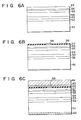
- Fig. 5 is a cross-sectional view showing an arrangement of a Burrus type LED according to a third embodiment of this invention
- Figs. 6A to 6C are cross-sectional views showing the steps of manufacturing the above-mentioned LED.
- This embodiment is different from the first embodiment in that the N-type clad layer is of a three-layer structure.
- an N-GaAs buffer layer 52, first clad layer 53 of N-GaAtAs, second clad layer 54 of N-GaAAAs, third clad layer 55 of N-GaAlAs, active layer 56 of P-GaAs and clad layer 57 of P-GaAtAs are grown by the MOCVD method on an N-GaAs substrate 51 in that order as shown in Fig. 6A.
- the mole traction, carrier concentration and depth of the respective layers are as shown in Table 2 below.
- Se and Zn were used as an N-type and a P-type dopant, respectively.
- the temperature for crystal growth was set at 750 [°C] under the condition that a better surface state is obtained.
- the above-mentioned numerical values are the most preferable examples, and can be properly varied according to the specification.
- the AlAs mole traction X, carrier concentration n and thickness of the first and second N-type clad layers 53 and 55 are 0.3 to 0.45 , 0 . 8 to 4 x 10 17 [cm -3 J and 1 to 3 [ ⁇ m], respectively, noting that these numerical values can properly be varied within these numeral ranges.
- the AtAs mixed crystal ratio X, carrier concentration and thickness of the second clad layer 54 are 0.1 to 0.25, 4 to 8 x 10 17 [cm -3 ] and 5 to 20 [ ⁇ m], respectively, noting that these numeral values can properly be varied within these ranges.
- ohmic electrode (contact metal) 58 made of AuZn (5 % Zn) was formed on the P-type clad layer 57, it was etched, with a I 2 -KI-H 2 0 (weight ratio: 1 : 1 : 4)-based etching solution, with a photoresist as a mask to leave a circular electrode 58 of 30 [um] in diameter.
- a 3,000 [A]-thick Si0 2 film 59 was formed by the CVD method on the surface of the P-side layer, followed by etching the Si0 2 film 59 on the ohmic electrode 58 with a photoresist as a mask by using an ammonium fluoride solution.
- a 1,000 [A] Cr layer and 5,000 [A] Au layer were formed on the surface of the P-side layer to form a P side electrode 60.
- an about 20 [um] heat sink 61 of Au was formed by an electroplating method on the surface of the P-side electrode 60.
- a 5,000 [A] layer of AuGe (0.5 % Ge) and 1,000 [A] layer of Au were evaporated on the rear surface of the substrate 51 to form an N-side electrode 62.
- the etching rate of GaAs in the substrate 51 and buffer layer 52 is about 10 times as fast as that of the first clad layer 53 (GaAtAs) of the N-type and, therefore, the first clad layer 53 acts as an etching stopper layer when the light pick-up window 63 is formed.
- the heat sink 61 is mounted on a stem, not shown.
- the forbidden band width of the N-type clad layers 53, 54 and 55 is greater than the forbidden band width of the active layer 56 and, therefore, light emitted from the active layer 56 is taken out without absorption at the interior of the LED structure.
- the confinement of carriers due to the presence of a double hetero-junction structure is carried out through the third clad layer 55, the reduction of the series resistance in the LED is carried out through the second clad layer 54 and the first clad layer 53 serves as an etching stopper layer when the light pick-up window is formed.
- the reason for this is as follows: That is, where the LED is manufactured by the MOCVD method, the carrier concentration of an N-Ga 1-x Al x As layer is not generally increased with an increase in the AtAs mixed crystal ratio X.
- injection carriers can be positively confined through the action of the third clad layer 55 and the spreading resistance can be decreased through the action of the second clad layer 54.
- This embodiment produces the same effect as that of the first embodiment of this invention. Furthermore, it is possible to beforehand prevent the light emission power from being dropped due to the influence of heat resulting from the series resistance at the LED. Therefore, a still higher output power can be assured due to such light emission characteristic.
- Fig. 7 is a cross-sectional view showing an arrangement of a Burrus type LED according to a fourth embodiment of this invention.
- the same reference numerals are employed to designate portions corresponding to those shown in Fig. 5, and, therefore, no further explanation is included for brevity.
- This embodiment is different from the third embodiment in that the N-type clad layer is formed as three or more layers. That is, a number of N-GaAlAs layers 73 1 , ..., 73 N are formed, as the N-type clad layers, between the N-type buffer layer 52 and the P-type active layer.
- those layers near the active layer 56 should be formed so that, in order to assure a positive confinement of injection carriers, the AlAs mole traction X is set to be higher than 0.3; the intermediate layer should be so formed that, in order to adequately raise the carrier concentration, the AlAs mixed crystal ratio X is set to be adequately small; and the layer in contact with the buffer layer 52 should be so formed that, in order to act as a stopper layer when the etching step is carried out, the AlAs mole traction X is set to be somewhat greater.
- the AlAs, mole traction X in the N-type clad layer can be varied in a step-like fashion to permit the mole traction X to vary in a near-continuous state.
- the N-type clad layer structure is not restricted to the three or more layer structure. That is, a two-layer structure may be adopted with the first clad layer omitted, provided that the etching rate of the second clad layer is sufficiently slower than that of the GaAs layers (the substrate and buffer layer) when an etching step is carried out.
- the Si0 2 film (the insulating film) formed on the above-mentioned clad layer to permit current to be narrowed use may be made of a semiconductor layer having a conductivity opposite to that of the above-mentioned clad layer.
- the semiconductor material which is used for the substrate and respective layers is not restricted to the GaAs/GaAlAs-based material only. It is also possible to use an InP/InGaAsP-based material or the other semiconductor material belonging to Group III-V compounds. This invention can be changed or modified in a variety of ways without departing from the spirit and scope of this invention.
Landscapes
- Led Devices (AREA)
Applications Claiming Priority (4)
| Application Number | Priority Date | Filing Date | Title |
|---|---|---|---|
| JP226154/84 | 1984-10-27 | ||
| JP59226154A JPS61104680A (ja) | 1984-10-27 | 1984-10-27 | 発光ダイオ−ドの製造方法 |
| JP16789/85 | 1985-01-31 | ||
| JP1678985A JPH0738458B2 (ja) | 1985-01-31 | 1985-01-31 | 半導体発光素子 |
Publications (3)
| Publication Number | Publication Date |
|---|---|
| EP0181448A2 true EP0181448A2 (de) | 1986-05-21 |
| EP0181448A3 EP0181448A3 (en) | 1986-11-05 |
| EP0181448B1 EP0181448B1 (de) | 1991-10-16 |
Family
ID=26353188
Family Applications (1)
| Application Number | Title | Priority Date | Filing Date |
|---|---|---|---|
| EP85110772A Expired - Lifetime EP0181448B1 (de) | 1984-10-27 | 1985-08-27 | Verfahren zur Herstellung einer lichtemittierenden Diode aus einem Verbindungshalbleiter |
Country Status (3)
| Country | Link |
|---|---|
| US (1) | US4706101A (de) |
| EP (1) | EP0181448B1 (de) |
| DE (1) | DE3584416D1 (de) |
Cited By (2)
| Publication number | Priority date | Publication date | Assignee | Title |
|---|---|---|---|---|
| EP0325493A3 (en) * | 1988-01-21 | 1990-08-22 | Mitsubishi Monsanto Chemical Company | Epitaxial substrate for high-intensity led, and method of manufacturing same |
| CN105845793A (zh) * | 2016-06-01 | 2016-08-10 | 天津三安光电有限公司 | 一种不可见光发光二极管及其制作方法 |
Families Citing this family (21)
| Publication number | Priority date | Publication date | Assignee | Title |
|---|---|---|---|---|
| US4870468A (en) * | 1986-09-12 | 1989-09-26 | Kabushiki Kaisha Toshiba | Semiconductor light-emitting device and method of manufacturing the same |
| NL8602653A (nl) * | 1986-10-23 | 1988-05-16 | Philips Nv | Halfgeleiderlaser en werkwijze ter vervaardiging daarvan. |
| JPH0278280A (ja) * | 1988-09-14 | 1990-03-19 | Ricoh Co Ltd | 半導体発光装置 |
| US4943970A (en) * | 1988-10-24 | 1990-07-24 | General Dynamics Corporation, Electronics Division | Surface emitting laser |
| US4901327A (en) * | 1988-10-24 | 1990-02-13 | General Dynamics Corporation, Electronics Division | Transverse injection surface emitting laser |
| US4873696A (en) * | 1988-10-31 | 1989-10-10 | The Regents Of The University Of California | Surface-emitting lasers with periodic gain and a parallel driven nipi structure |
| FR2640438B1 (fr) * | 1988-12-09 | 1991-01-25 | Thomson Csf | Procede de realisation de lasers semi-conducteurs et lasers obtenus par le procede |
| US5038356A (en) * | 1989-12-04 | 1991-08-06 | Trw Inc. | Vertical-cavity surface-emitting diode laser |
| SE468410B (sv) * | 1991-05-08 | 1993-01-11 | Asea Brown Boveri | Ytlysande lysdiod |
| JP3374878B2 (ja) * | 1994-09-02 | 2003-02-10 | 三菱電機株式会社 | 半導体エッチング方法 |
| US9586526B2 (en) * | 1995-04-21 | 2017-03-07 | Magna Mirrors Of America, Inc. | Vehicle exterior mirror system |
| US6633120B2 (en) * | 1998-11-19 | 2003-10-14 | Unisplay S.A. | LED lamps |
| US8587020B2 (en) | 1997-11-19 | 2013-11-19 | Epistar Corporation | LED lamps |
| DE10039945B4 (de) * | 2000-08-16 | 2006-07-13 | Vishay Semiconductor Gmbh | Verfahren zum Herstellen einer lichtemittierenden Halbleiteranordnung aus GaAIAs mit Doppelheterostruktur und entsprechende Halbleiteranordnung |
| JP3910817B2 (ja) * | 2000-12-19 | 2007-04-25 | ユーディナデバイス株式会社 | 半導体受光装置 |
| US7233028B2 (en) * | 2001-02-23 | 2007-06-19 | Nitronex Corporation | Gallium nitride material devices and methods of forming the same |
| AU2003227230A1 (en) * | 2002-04-04 | 2003-10-20 | Sharp Kabushiki Kaisha | Semiconductor laser device |
| JP4074498B2 (ja) * | 2002-09-25 | 2008-04-09 | セイコーエプソン株式会社 | 面発光型発光素子、光モジュールおよび光伝達装置 |
| US8513688B2 (en) * | 2009-12-02 | 2013-08-20 | Walsin Lihwa Corporation | Method for enhancing electrical injection efficiency and light extraction efficiency of light-emitting devices |
| CN102117871A (zh) * | 2009-12-31 | 2011-07-06 | 华新丽华股份有限公司 | 增益发光装置的电注入效率和出光效率的方法 |
| FR3069106B1 (fr) * | 2017-07-17 | 2019-10-18 | Commissariat A L'energie Atomique Et Aux Energies Alternatives | Diode electroluminescente comportant un empilement a partie amincie et procede d'elaboration de la diode electroluminescente |
Family Cites Families (4)
| Publication number | Priority date | Publication date | Assignee | Title |
|---|---|---|---|---|
| US3936855A (en) * | 1974-08-08 | 1976-02-03 | International Telephone And Telegraph Corporation | Light-emitting diode fabrication process |
| GB1478152A (en) * | 1974-10-03 | 1977-06-29 | Standard Telephones Cables Ltd | Light emissive diode |
| US4184170A (en) * | 1977-02-11 | 1980-01-15 | Xerox Corporation | Light emitting diode |
| US4447822A (en) * | 1981-09-21 | 1984-05-08 | Bell Telephone Laboratories, Incorporated | Light emitting diode |
-
1985
- 1985-08-20 US US06/767,425 patent/US4706101A/en not_active Expired - Lifetime
- 1985-08-27 DE DE8585110772T patent/DE3584416D1/de not_active Expired - Lifetime
- 1985-08-27 EP EP85110772A patent/EP0181448B1/de not_active Expired - Lifetime
Cited By (2)
| Publication number | Priority date | Publication date | Assignee | Title |
|---|---|---|---|---|
| EP0325493A3 (en) * | 1988-01-21 | 1990-08-22 | Mitsubishi Monsanto Chemical Company | Epitaxial substrate for high-intensity led, and method of manufacturing same |
| CN105845793A (zh) * | 2016-06-01 | 2016-08-10 | 天津三安光电有限公司 | 一种不可见光发光二极管及其制作方法 |
Also Published As
| Publication number | Publication date |
|---|---|
| US4706101A (en) | 1987-11-10 |
| DE3584416D1 (de) | 1991-11-21 |
| EP0181448A3 (en) | 1986-11-05 |
| EP0181448B1 (de) | 1991-10-16 |
Similar Documents
| Publication | Publication Date | Title |
|---|---|---|
| US4706101A (en) | Light emitting diode formed of a compound semiconductor material | |
| US6278137B1 (en) | Semiconductor light-emitting devices | |
| US5153889A (en) | Semiconductor light emitting device | |
| EP0356037B1 (de) | Verfahren zur Herstellung einer elektro-optischen Vorrichtung mit einem umgekehrten durchsichtigen Substrat | |
| US5932896A (en) | Nitride system semiconductor device with oxygen | |
| JP3276641B2 (ja) | 発光半導体装置及びその製造方法 | |
| US5115286A (en) | Electro-optical device with inverted transparent substrate and method for making same | |
| KR100912622B1 (ko) | 반도체 광소자의 제조 방법 | |
| US4503539A (en) | Semiconductor laser | |
| US20040021142A1 (en) | Light emitting diode device | |
| US4810670A (en) | Method of manufacturing an embedded type semiconductor laser | |
| EP0293000B1 (de) | Lichtemittierende Vorrichtung | |
| US7230281B2 (en) | Semiconductor light emitting device | |
| JPH11284280A (ja) | 半導体レーザ装置及びその製造方法ならびにiii−v族化合物半導体素子の製造方法 | |
| JPH05218498A (ja) | 横方向に接合を有する発光ダイオード | |
| EP0140645B1 (de) | Lichtemittierende Halbleitervorrichtung | |
| KR890004477B1 (ko) | 발광 다이오드의 제조방법 | |
| JPH0945959A (ja) | 発光素子 | |
| JP3141888B2 (ja) | 半導体発光素子 | |
| JP2002164569A (ja) | 発光素子用エピタキシャルウェハ及び発光素子 | |
| JPH09172198A (ja) | 発光ダイオードおよびその製造方法 | |
| JP3139886B2 (ja) | 半導体レーザ素子およびその製造方法 | |
| JPH05218585A (ja) | 半導体発光装置 | |
| JP2004356600A (ja) | 半導体発光素子 | |
| JPH0572118B2 (de) |
Legal Events
| Date | Code | Title | Description |
|---|---|---|---|
| PUAI | Public reference made under article 153(3) epc to a published international application that has entered the european phase |
Free format text: ORIGINAL CODE: 0009012 |
|
| 17P | Request for examination filed |
Effective date: 19850924 |
|
| AK | Designated contracting states |
Kind code of ref document: A2 Designated state(s): DE FR GB |
|
| PUAL | Search report despatched |
Free format text: ORIGINAL CODE: 0009013 |
|
| AK | Designated contracting states |
Kind code of ref document: A3 Designated state(s): DE FR GB |
|
| 17Q | First examination report despatched |
Effective date: 19890215 |
|
| GRAA | (expected) grant |
Free format text: ORIGINAL CODE: 0009210 |
|
| AK | Designated contracting states |
Kind code of ref document: B1 Designated state(s): DE FR GB |
|
| REF | Corresponds to: |
Ref document number: 3584416 Country of ref document: DE Date of ref document: 19911121 |
|
| ET | Fr: translation filed | ||
| PLBE | No opposition filed within time limit |
Free format text: ORIGINAL CODE: 0009261 |
|
| STAA | Information on the status of an ep patent application or granted ep patent |
Free format text: STATUS: NO OPPOSITION FILED WITHIN TIME LIMIT |
|
| 26N | No opposition filed | ||
| PGFP | Annual fee paid to national office [announced via postgrant information from national office to epo] |
Ref country code: GB Payment date: 19970818 Year of fee payment: 13 |
|
| PGFP | Annual fee paid to national office [announced via postgrant information from national office to epo] |
Ref country code: DE Payment date: 19970905 Year of fee payment: 13 |
|
| PG25 | Lapsed in a contracting state [announced via postgrant information from national office to epo] |
Ref country code: GB Free format text: LAPSE BECAUSE OF NON-PAYMENT OF DUE FEES Effective date: 19980827 |
|
| GBPC | Gb: european patent ceased through non-payment of renewal fee |
Effective date: 19980827 |
|
| REG | Reference to a national code |
Ref country code: FR Ref legal event code: D6 |
|
| PG25 | Lapsed in a contracting state [announced via postgrant information from national office to epo] |
Ref country code: DE Free format text: LAPSE BECAUSE OF NON-PAYMENT OF DUE FEES Effective date: 19990601 |
|
| PGFP | Annual fee paid to national office [announced via postgrant information from national office to epo] |
Ref country code: FR Payment date: 20040810 Year of fee payment: 20 |