EP0143607B1 - Empaquetage pour semi-conducteur - Google Patents
Empaquetage pour semi-conducteur Download PDFInfo
- Publication number
- EP0143607B1 EP0143607B1 EP84308084A EP84308084A EP0143607B1 EP 0143607 B1 EP0143607 B1 EP 0143607B1 EP 84308084 A EP84308084 A EP 84308084A EP 84308084 A EP84308084 A EP 84308084A EP 0143607 B1 EP0143607 B1 EP 0143607B1
- Authority
- EP
- European Patent Office
- Prior art keywords
- base
- cap
- semiconductor device
- metallization
- insulating
- Prior art date
- Legal status (The legal status is an assumption and is not a legal conclusion. Google has not performed a legal analysis and makes no representation as to the accuracy of the status listed.)
- Expired
Links
Images


Classifications
-
- H—ELECTRICITY
- H10—SEMICONDUCTOR DEVICES; ELECTRIC SOLID-STATE DEVICES NOT OTHERWISE PROVIDED FOR
- H10W—GENERIC PACKAGES, INTERCONNECTIONS, CONNECTORS OR OTHER CONSTRUCTIONAL DETAILS OF DEVICES COVERED BY CLASS H10
- H10W70/00—Package substrates; Interposers; Redistribution layers [RDL]
- H10W70/60—Insulating or insulated package substrates; Interposers; Redistribution layers
-
- H—ELECTRICITY
- H10—SEMICONDUCTOR DEVICES; ELECTRIC SOLID-STATE DEVICES NOT OTHERWISE PROVIDED FOR
- H10W—GENERIC PACKAGES, INTERCONNECTIONS, CONNECTORS OR OTHER CONSTRUCTIONAL DETAILS OF DEVICES COVERED BY CLASS H10
- H10W74/00—Encapsulations, e.g. protective coatings
- H10W74/01—Manufacture or treatment
-
- H—ELECTRICITY
- H10—SEMICONDUCTOR DEVICES; ELECTRIC SOLID-STATE DEVICES NOT OTHERWISE PROVIDED FOR
- H10W—GENERIC PACKAGES, INTERCONNECTIONS, CONNECTORS OR OTHER CONSTRUCTIONAL DETAILS OF DEVICES COVERED BY CLASS H10
- H10W70/00—Package substrates; Interposers; Redistribution layers [RDL]
- H10W70/60—Insulating or insulated package substrates; Interposers; Redistribution layers
- H10W70/67—Insulating or insulated package substrates; Interposers; Redistribution layers characterised by their insulating layers or insulating parts
- H10W70/68—Shapes or dispositions thereof
-
- H—ELECTRICITY
- H10—SEMICONDUCTOR DEVICES; ELECTRIC SOLID-STATE DEVICES NOT OTHERWISE PROVIDED FOR
- H10W—GENERIC PACKAGES, INTERCONNECTIONS, CONNECTORS OR OTHER CONSTRUCTIONAL DETAILS OF DEVICES COVERED BY CLASS H10
- H10W72/00—Interconnections or connectors in packages
- H10W72/071—Connecting or disconnecting
-
- H—ELECTRICITY
- H10—SEMICONDUCTOR DEVICES; ELECTRIC SOLID-STATE DEVICES NOT OTHERWISE PROVIDED FOR
- H10W—GENERIC PACKAGES, INTERCONNECTIONS, CONNECTORS OR OTHER CONSTRUCTIONAL DETAILS OF DEVICES COVERED BY CLASS H10
- H10W76/00—Containers; Fillings or auxiliary members therefor; Seals
- H10W76/60—Seals
-
- H—ELECTRICITY
- H10—SEMICONDUCTOR DEVICES; ELECTRIC SOLID-STATE DEVICES NOT OTHERWISE PROVIDED FOR
- H10W—GENERIC PACKAGES, INTERCONNECTIONS, CONNECTORS OR OTHER CONSTRUCTIONAL DETAILS OF DEVICES COVERED BY CLASS H10
- H10W70/00—Package substrates; Interposers; Redistribution layers [RDL]
- H10W70/60—Insulating or insulated package substrates; Interposers; Redistribution layers
- H10W70/67—Insulating or insulated package substrates; Interposers; Redistribution layers characterised by their insulating layers or insulating parts
- H10W70/68—Shapes or dispositions thereof
- H10W70/682—Shapes or dispositions thereof comprising holes having chips therein
-
- H—ELECTRICITY
- H10—SEMICONDUCTOR DEVICES; ELECTRIC SOLID-STATE DEVICES NOT OTHERWISE PROVIDED FOR
- H10W—GENERIC PACKAGES, INTERCONNECTIONS, CONNECTORS OR OTHER CONSTRUCTIONAL DETAILS OF DEVICES COVERED BY CLASS H10
- H10W72/00—Interconnections or connectors in packages
- H10W72/50—Bond wires
- H10W72/551—Materials of bond wires
- H10W72/552—Materials of bond wires comprising metals or metalloids, e.g. silver
- H10W72/5522—Materials of bond wires comprising metals or metalloids, e.g. silver comprising gold [Au]
-
- H—ELECTRICITY
- H10—SEMICONDUCTOR DEVICES; ELECTRIC SOLID-STATE DEVICES NOT OTHERWISE PROVIDED FOR
- H10W—GENERIC PACKAGES, INTERCONNECTIONS, CONNECTORS OR OTHER CONSTRUCTIONAL DETAILS OF DEVICES COVERED BY CLASS H10
- H10W72/00—Interconnections or connectors in packages
- H10W72/50—Bond wires
- H10W72/551—Materials of bond wires
- H10W72/552—Materials of bond wires comprising metals or metalloids, e.g. silver
- H10W72/5524—Materials of bond wires comprising metals or metalloids, e.g. silver comprising aluminium [Al]
-
- H—ELECTRICITY
- H10—SEMICONDUCTOR DEVICES; ELECTRIC SOLID-STATE DEVICES NOT OTHERWISE PROVIDED FOR
- H10W—GENERIC PACKAGES, INTERCONNECTIONS, CONNECTORS OR OTHER CONSTRUCTIONAL DETAILS OF DEVICES COVERED BY CLASS H10
- H10W76/00—Containers; Fillings or auxiliary members therefor; Seals
- H10W76/10—Containers or parts thereof
- H10W76/17—Containers or parts thereof characterised by their materials
- H10W76/18—Insulating materials, e.g. resins, glasses or ceramics
-
- H—ELECTRICITY
- H10—SEMICONDUCTOR DEVICES; ELECTRIC SOLID-STATE DEVICES NOT OTHERWISE PROVIDED FOR
- H10W—GENERIC PACKAGES, INTERCONNECTIONS, CONNECTORS OR OTHER CONSTRUCTIONAL DETAILS OF DEVICES COVERED BY CLASS H10
- H10W90/00—Package configurations
- H10W90/701—Package configurations characterised by the relative positions of pads or connectors relative to package parts
- H10W90/751—Package configurations characterised by the relative positions of pads or connectors relative to package parts of bond wires
- H10W90/754—Package configurations characterised by the relative positions of pads or connectors relative to package parts of bond wires between a chip and a stacked insulating package substrate, interposer or RDL
Definitions
- the present invention relates to a semiconductor device, more particularly, to a semiconductor device including a semiconductor chip in a cavity on a ceramic base and a ceramic cap sealing the cavity.
- the cap is preferably made of ceramic.
- the cap is bonded to the base by metallizing the two in the regions of contact and soldering them in the metallized regions. Soldering is carried out by inserting a thin ring pattern of solder between the ceramic base and cap, melting the solder while simultaneously pressing the cap against the base, and then cooling. The pressing of the cap is effected to prevent formation of voids in the soldering portion between the base and the cap since a ceramic cap is often somewhat warped.
- Japanese Unexamined Patent Publication (Kokai) No. 55-148445 disclosed formation of a separate pattern of metallization in addition to a pattern of metallization for soldering on an inner surface of a ceramic cap.
- the separate metallization pattern is formed on a portion of the cap spaced from and inward from the metallization pattern provided for soldering the surface of the cap facing the base.
- This separate metallization pattern is, however, not very effective for preventing the flow or the flight of excess solder toward the outside of the cap and the base and into a cavity of the base. Also, the problem of seal quality between the cap and the base is not solved by this separate pattern of metallization.
- the object of the present invention is to provide a semiconductor device comprised of an insulating base carrying a semiconductor chip and an insulating cap sealed to the insulating base and in which the soldering of the insulating base to the insulating cap is effected with reduced flow or flight of excess solder.
- a semiconductor device comprising a semiconductor chip, an insulating base having a cavity for carrying the semiconductor chip, and an insulating cap covering and sealing the cavity of the insulating base, and in which the insulating base and the insulating cap have patterns of metallization in areas of contact therebetween, characterized in that the pattern of metallization of the insulating cap extends from the area of contact between the base and the cap to include at least a portion of the side surfaces of the insulating cap, the insulating base and the insulating cap being soldered to each other in the areas of the patterns of metallization.
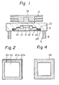
- FIG. 1 illustrates a preferred embodiment of a semiconductor device embodying the present invention.
- the semiconductor device comprises a ceramic base 2 of, e.g., alumina having a cavity 4, a semiconductor chip 6 mounted on the base 2 at the bottom of the cavity 4, a plurality of lead pins 8 of, e.g., an iron-nickel alloy provided on the base 2 on the side where the cavity 4 is opened, a ceramic cap 10 of, e.g., alumina covering the cavity 4, and a cooling fin 12 provided on the base 2 on the side opposite to the lead pins 8.
- the semiconductor chip 6 is mounted onto a metallized dice stage of, e.g., tungsten plated by nickel and gold, which stage is on the surface of the base 2 at the bottom of the cavity 4.
- the semiconductor chip 6 is electrically connected to the lead pins 8 by means of fine wires 14 of, e.g., gold or aluminium and through metallization patterns 16, of e.g., tungsten running in the ceramic base 2.
- the fine wires are bonded to each of the metallization patterns 16 and to each of terminals of the semiconductor chip 6.
- the metallization patterns 16 in the base reach the lead pins 8.
- the cooling fin 12 is attached to the base 2 with a member 18 bonded to the base 2 for carrying the cooling fin 12.
- the ceramic cap 10 and the ceramic base 2 have metallization patterns 20 and 22 respectively in regions where they contact each other.
- the metallization pattern 20 of the cap 10 extends not only to a region of the main inner surface of the cap 10 where the cap 10 contacts the base 2, but also to the four side surfaces of the cap 10.
- the ceramic cap 10 has a metallization pattern 20 including a pattern 20a on the main surface of the cap 10 along the periphery thereof, the central square or rectangular portion of the cap 10 not being covered, and a pattern 20b on the four side surfaces of the cap 10.
- This metallization pattern 20 is made, for example, by screen printing, e.g., tungsten paste onto the surfaces of a green ceramic cap five times, once for the main surface and four times for the four side surfaces, then firing the green cap 10 and plating nickel and gold layers on the surface of the tungsten pattern.
- the ceramic base 2 has a metallized dice stage 24 at the bottom of the cavity 4, metallization patterns 16 running in the ceramic base 2 and extending onto an intermediate stage in the cavity 4, and a metallization pattern 22 for soldering on the surface of a cap-receiving stage, the cap-receiving stage being slightly lower than the top surface of the base 10 in order to make the top surfaces of the base 2 and the cap 10 even.
- the base is made, for example, by shaping green ceramic sheets, screen printing and pouring metal paste on the surface and in pores of the green sheets, laminating the green sheets, and firing the lamination of the green sheets to sinter them.
- the outer edges of the metallization pattern 22 of the base 2 preferably extend slightly more outward than the cap 10. This allows formation of a meniscus by excess solder at the corners formed by the metallized top surface of the base 2 and the metallized side surfaces of the cap 10.
- the inner edges of the metallization pattern 22 preferably do not enter all the way to the edges of the cavity 4. This prevents overflow of metal paste into the cavity 4 due to misalignment of a screen with the cap receiving portion of the base when metal paste is screen printed.
- the inner edges of the metallization pattern 20 of the cap 10 preferably extend further inward than the inner edges of the metallization pattern 22 of the base 2. This enables thorough contact between the metallization patterns 20 and 22, even if alignment between them is not complete.
- a thin solder pattern 26 (Fig. 4) of, e.g., a gold-tin alloy (or a lead-tin alloy) 70 pm thick is inserted between the metallization patterns 20 and 22 of the base 2 and the cap 10.
- the volume of the solder pattern is calculated to conform with the required volume. Applying pressure of approximately 1 x 10 5 Pa toward the cap 10, the assembly of the base 2, the solder pattern 26, and the cap 10 is heated to a temperature of 330°C and then cooled to solidify the solder (28 in Fig. 1).
- the lead pins 8 are not illustrated in Figs. 3a and 3b for simplicity.
- the extended metallization portion absorbs excess solder but the extended metallization portion, if too large, often absorbs the solder necessary to seal the space between the cap and the base, resulting in the formation of voids in the soldering.
- Figure 5 illustrates another embodiment of a semiconductor device according to the present invention.
- This device is the same as that in Fig. 1 except that the base 2 has a metallization pattern 32 which exists not only in the area where the base 2 is in contact with the cap 10 but also on the surfaces of the side walls of the recess of the base 2 for receiving the cap 10 to make the top surfaces of the cap 10 and the base 2 even.
- a meniscus of solder may also be formed between the two metallization patterns 20 and 32 of the cap 10 and the base 2.
- FIG. 6 illustrates a further embodiment of a semiconductor device according to the present invention.
- This semiconductor device is similar to the semicoductor device in Fig. 1. Parts of this semiconductor device similar to those in Fig. 1 are indicated by the same reference numerals.
- no cooling fin is attached to a ceramic base 42
- a plurality of lead pins 8 are provided on the rear side of the base 42 opposite to the side where a cavity 4 opens and a ceramic cap 10 is emplaced, and the top surface of the cap 10 is not even with the top surface of the base 42.
- soldering metallization patterns of the ceramic cap and the ceramic base may be different from those described before.
- the inner edges of the metallization pattern of the cap may extend only to a point outward from the inner edges of the metallization pattern of the base or just up to those inner edges.
- the inner edges of the metallization of the cap may extend to the edges of the cavity of the base or further inward.
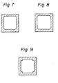
- the shape of the metallization pattern of the cap may be strictly square or rectangular or, for example, of the shapes shown in Figures 7 to 9.
- the ceramic cap 10 may be a disc and the metallization of the cap 10 is consequently in the form of a ring.
- the materials of the cap, base metallizations, and solder and the process for fabricating a semiconductor device may be different from those described before.
- alumina is the most preferable at present, other materials such as alumina with added ingredients, such as beryllium oxide BeO or silicon carbide SiC are also applicable.
- a ceramic package of a so-called Pin Grid Array is illustrated. Metal pads such as solder pads may be used instead of the pins 8.
Landscapes
- Lead Frames For Integrated Circuits (AREA)
- Cooling Or The Like Of Semiconductors Or Solid State Devices (AREA)
- Wire Bonding (AREA)
Claims (12)
Applications Claiming Priority (2)
| Application Number | Priority Date | Filing Date | Title |
|---|---|---|---|
| JP58222191A JPS60115247A (ja) | 1983-11-28 | 1983-11-28 | 半導体装置 |
| JP222191/83 | 1983-11-28 |
Publications (3)
| Publication Number | Publication Date |
|---|---|
| EP0143607A2 EP0143607A2 (fr) | 1985-06-05 |
| EP0143607A3 EP0143607A3 (en) | 1986-10-22 |
| EP0143607B1 true EP0143607B1 (fr) | 1989-01-18 |
Family
ID=16778575
Family Applications (1)
| Application Number | Title | Priority Date | Filing Date |
|---|---|---|---|
| EP84308084A Expired EP0143607B1 (fr) | 1983-11-28 | 1984-11-21 | Empaquetage pour semi-conducteur |
Country Status (6)
| Country | Link |
|---|---|
| US (1) | US4626960A (fr) |
| EP (1) | EP0143607B1 (fr) |
| JP (1) | JPS60115247A (fr) |
| KR (1) | KR850004174A (fr) |
| DE (1) | DE3476296D1 (fr) |
| IE (1) | IE56188B1 (fr) |
Families Citing this family (38)
| Publication number | Priority date | Publication date | Assignee | Title |
|---|---|---|---|---|
| GB2167906B (en) * | 1984-11-23 | 1988-08-10 | Gec Avionics | Rack mounted circuit module |
| JPS6256597A (ja) * | 1985-09-06 | 1987-03-12 | Hitachi Ltd | 電子部品のメツキ方法 |
| US4640438A (en) * | 1986-03-17 | 1987-02-03 | Comienco Limited | Cover for semiconductor device packages |
| US4802718A (en) * | 1986-09-03 | 1989-02-07 | Grumman Aerospace Corporation | One piece frame for holding a holographic element in a holographic system |
| JPH0777247B2 (ja) * | 1986-09-17 | 1995-08-16 | 富士通株式会社 | 半導体装置の製造方法 |
| US4746583A (en) * | 1986-11-21 | 1988-05-24 | Indium Corporation | Ceramic combined cover |
| US4785827A (en) * | 1987-01-28 | 1988-11-22 | Minnesota Mining And Manufacturing Company | Subcutaneous housing assembly |
| US4796156A (en) * | 1987-12-04 | 1989-01-03 | General Electric Company | Self packaging chip mount |
| US4833568A (en) * | 1988-01-29 | 1989-05-23 | Berhold G Mark | Three-dimensional circuit component assembly and method corresponding thereto |
| US4857988A (en) * | 1988-02-09 | 1989-08-15 | Fottler Stanley A | Leadless ceramic chip carrier |
| US5184211A (en) * | 1988-03-01 | 1993-02-02 | Digital Equipment Corporation | Apparatus for packaging and cooling integrated circuit chips |
| JPH02180053A (ja) * | 1988-12-30 | 1990-07-12 | Narumi China Corp | 半導体パッケージ用リード基板 |
| JPH02142536U (fr) * | 1989-04-28 | 1990-12-04 | ||
| EP0435155B1 (fr) * | 1989-12-29 | 1994-06-01 | Sumitomo Electric Industries, Ltd. | Dissipateur de chaleur ayant une longévité améliorée et une conductibilité thermique |
| US5556810A (en) * | 1990-06-01 | 1996-09-17 | Kabushiki Kaisha Toshiba | Method for manufacturing a semiconductor device wherein a semiconductor chip is connected to a lead frame by metal plating |
| JP2540652B2 (ja) * | 1990-06-01 | 1996-10-09 | 株式会社東芝 | 半導体装置 |
| US5270491A (en) * | 1990-10-09 | 1993-12-14 | Eastman Kodak Company | Hermetically sealed microelectronic package |
| JPH10501656A (ja) * | 1992-01-27 | 1998-02-10 | ハリス・コーポレーション | 半導体デバイス及びその量産方法 |
| EP0608418B1 (fr) * | 1992-05-20 | 1998-11-04 | Seiko Epson Corporation | Cartouche destinee a un appareil electronique |
| US8213431B2 (en) * | 2008-01-18 | 2012-07-03 | The Boeing Company | System and method for enabling wireless real time applications over a wide area network in high signal intermittence environments |
| US5353193A (en) * | 1993-02-26 | 1994-10-04 | Lsi Logic Corporation | High power dissipating packages with matched heatspreader heatsink assemblies |
| US5821455A (en) * | 1993-04-26 | 1998-10-13 | Sumitomo Metal (Smi) Electronics Devices, Inc. | Lid with variable solder layer for sealing semiconductor package, package having the lid and method for producing the lid |
| US5367193A (en) * | 1993-06-17 | 1994-11-22 | Sun Microsystems, Inc. | Low cost, thermally efficient, and surface mountable semiconductor package for a high applied power VLSI die |
| JP3417608B2 (ja) * | 1993-08-03 | 2003-06-16 | 日本特殊陶業株式会社 | 半導体パッケージ用のセラミック製リッド基板 |
| JP3369665B2 (ja) * | 1993-08-27 | 2003-01-20 | 日本特殊陶業株式会社 | 半導体パッケージ用のセラミック製リッド基板およびセラミック製リッド |
| US5477409A (en) * | 1993-11-24 | 1995-12-19 | Vlsi Technology Inc. | Fusion heat sink for integrated circuit |
| US5498900A (en) * | 1993-12-22 | 1996-03-12 | Honeywell Inc. | Semiconductor package with weldable ceramic lid |
| US5917239A (en) * | 1995-11-30 | 1999-06-29 | Intel Corporation | Recessed or raised characters on a ceramic lid |
| US6753922B1 (en) | 1998-10-13 | 2004-06-22 | Intel Corporation | Image sensor mounted by mass reflow |
| DE19983826T1 (de) * | 1998-12-21 | 2002-03-07 | Intel Corp | Mit einem Fenster versehenes nicht-keramisches Gehäuse mit einem eingebetteten Rahmen |
| US6262479B1 (en) * | 1999-10-05 | 2001-07-17 | Pan Pacific Semiconductor Co., Ltd. | Semiconductor packaging structure |
| US6352935B1 (en) | 2000-01-18 | 2002-03-05 | Analog Devices, Inc. | Method of forming a cover cap for semiconductor wafer devices |
| GB2372473B (en) * | 2001-02-24 | 2003-04-16 | Marconi Caswell Ltd | A method of soldering |
| JP4511278B2 (ja) * | 2004-08-11 | 2010-07-28 | 三洋電機株式会社 | セラミックパッケージ |
| FR2890065B1 (fr) * | 2005-08-30 | 2007-09-21 | Commissariat Energie Atomique | Procede d'encapsulation d'un composant, notamment electrique ou electronique au moyen d'un cordon de soudure ameliore |
| JP6028592B2 (ja) | 2013-01-25 | 2016-11-16 | 三菱電機株式会社 | 半導体装置 |
| JP2015192097A (ja) * | 2014-03-28 | 2015-11-02 | 住友電工デバイス・イノベーション株式会社 | 電子部品搭載用パッケージ |
| CN117139767B (zh) * | 2023-10-27 | 2023-12-26 | 合肥先进封装陶瓷有限公司 | 一种陶瓷封壳体输送装置及其装配设备 |
Family Cites Families (4)
| Publication number | Priority date | Publication date | Assignee | Title |
|---|---|---|---|---|
| US3943557A (en) * | 1974-02-19 | 1976-03-09 | Plessey Incorporated | Semiconductor package with integral hermeticity detector |
| JPS55148445A (en) * | 1979-05-10 | 1980-11-19 | Nec Corp | Semiconductor device |
| JPS57192054A (en) * | 1981-05-22 | 1982-11-26 | Hitachi Ltd | Heat radiating structure of leadless package |
| JPS58158950A (ja) * | 1982-03-16 | 1983-09-21 | Nec Corp | 半導体装置 |
-
1983
- 1983-11-28 JP JP58222191A patent/JPS60115247A/ja active Pending
-
1984
- 1984-11-21 DE DE8484308084T patent/DE3476296D1/de not_active Expired
- 1984-11-21 EP EP84308084A patent/EP0143607B1/fr not_active Expired
- 1984-11-27 IE IE3034/84A patent/IE56188B1/en not_active IP Right Cessation
- 1984-11-28 US US06/675,795 patent/US4626960A/en not_active Expired - Lifetime
- 1984-11-28 KR KR1019840007462A patent/KR850004174A/ko not_active Ceased
Also Published As
| Publication number | Publication date |
|---|---|
| JPS60115247A (ja) | 1985-06-21 |
| EP0143607A3 (en) | 1986-10-22 |
| EP0143607A2 (fr) | 1985-06-05 |
| IE843034L (en) | 1985-05-28 |
| KR850004174A (ko) | 1985-07-01 |
| DE3476296D1 (en) | 1989-02-23 |
| IE56188B1 (en) | 1991-05-08 |
| US4626960A (en) | 1986-12-02 |
Similar Documents
| Publication | Publication Date | Title |
|---|---|---|
| US4626960A (en) | Semiconductor device having soldered bond between base and cap thereof | |
| KR100480515B1 (ko) | 반도체 장치 | |
| EP0627766B1 (fr) | Dispositif semi-conducteur et méthode pour sa fabrication | |
| US6486551B1 (en) | Wired board and method of producing the same | |
| US5296737A (en) | Semiconductor device with a plurality of face to face chips | |
| US5970320A (en) | Process of resin sealing a semiconductor device and lead frame | |
| US4677741A (en) | Method of manufacturing package for high power integrated circuit | |
| US4857988A (en) | Leadless ceramic chip carrier | |
| JP3327452B2 (ja) | 電子部品用パッケージ | |
| JP4384339B2 (ja) | 連結セラミック配線基板の製造方法、および配線基板の製造方法。 | |
| JP2001319991A (ja) | 連結セラミック配線基板 | |
| JP4184632B2 (ja) | 電子部品パッケージ及びそれに使用するセラミック製端子台の製造方法 | |
| EP0474224B1 (fr) | Dispositif semi-conducteur comprenant une pluralité de puces semi-conductrices | |
| JPH0714942A (ja) | 半導体装置 | |
| TWI869699B (zh) | 配線基板及電子裝置 | |
| JPS6336688Y2 (fr) | ||
| JP2602834B2 (ja) | 半導体装置 | |
| JP2001185638A (ja) | セラミック積層構造の配線基板 | |
| JP2702455B2 (ja) | ピングリッドアレイ型半導体装置 | |
| JP3359521B2 (ja) | 半導体装置の製造方法 | |
| JPS6233342Y2 (fr) | ||
| EP0762494B1 (fr) | Diode semi-conductrice en silicium, son module de circuit et structure avec un corps isolant et procédé de préparation | |
| JPS5940774Y2 (ja) | マルチチツプ集積回路の気密実装構造 | |
| JP3441170B2 (ja) | 配線基板 | |
| JPH08162589A (ja) | 半導体装置 |
Legal Events
| Date | Code | Title | Description |
|---|---|---|---|
| PUAI | Public reference made under article 153(3) epc to a published international application that has entered the european phase |
Free format text: ORIGINAL CODE: 0009012 |
|
| AK | Designated contracting states |
Designated state(s): DE FR GB |
|
| PUAL | Search report despatched |
Free format text: ORIGINAL CODE: 0009013 |
|
| AK | Designated contracting states |
Kind code of ref document: A3 Designated state(s): DE FR GB |
|
| 17P | Request for examination filed |
Effective date: 19870313 |
|
| 17Q | First examination report despatched |
Effective date: 19880215 |
|
| GRAA | (expected) grant |
Free format text: ORIGINAL CODE: 0009210 |
|
| AK | Designated contracting states |
Kind code of ref document: B1 Designated state(s): DE FR GB |
|
| REF | Corresponds to: |
Ref document number: 3476296 Country of ref document: DE Date of ref document: 19890223 |
|
| ET | Fr: translation filed | ||
| PLBE | No opposition filed within time limit |
Free format text: ORIGINAL CODE: 0009261 |
|
| STAA | Information on the status of an ep patent application or granted ep patent |
Free format text: STATUS: NO OPPOSITION FILED WITHIN TIME LIMIT |
|
| 26N | No opposition filed | ||
| PGFP | Annual fee paid to national office [announced via postgrant information from national office to epo] |
Ref country code: FR Payment date: 19981110 Year of fee payment: 15 |
|
| PGFP | Annual fee paid to national office [announced via postgrant information from national office to epo] |
Ref country code: GB Payment date: 19981127 Year of fee payment: 15 |
|
| PGFP | Annual fee paid to national office [announced via postgrant information from national office to epo] |
Ref country code: DE Payment date: 19981130 Year of fee payment: 15 |
|
| PG25 | Lapsed in a contracting state [announced via postgrant information from national office to epo] |
Ref country code: GB Free format text: LAPSE BECAUSE OF NON-PAYMENT OF DUE FEES Effective date: 19991121 |
|
| GBPC | Gb: european patent ceased through non-payment of renewal fee |
Effective date: 19991121 |
|
| PG25 | Lapsed in a contracting state [announced via postgrant information from national office to epo] |
Ref country code: FR Free format text: LAPSE BECAUSE OF NON-PAYMENT OF DUE FEES Effective date: 20000731 |
|
| PG25 | Lapsed in a contracting state [announced via postgrant information from national office to epo] |
Ref country code: DE Free format text: LAPSE BECAUSE OF NON-PAYMENT OF DUE FEES Effective date: 20000901 |
|
| REG | Reference to a national code |
Ref country code: FR Ref legal event code: ST |