EP0144828A1 - Dispositif de commande d'un élément à cristal liquide - Google Patents
Dispositif de commande d'un élément à cristal liquide Download PDFInfo
- Publication number
- EP0144828A1 EP0144828A1 EP84113754A EP84113754A EP0144828A1 EP 0144828 A1 EP0144828 A1 EP 0144828A1 EP 84113754 A EP84113754 A EP 84113754A EP 84113754 A EP84113754 A EP 84113754A EP 0144828 A1 EP0144828 A1 EP 0144828A1
- Authority
- EP
- European Patent Office
- Prior art keywords
- voltage
- circuit
- liquid crystal
- crystal element
- output voltage
- Prior art date
- Legal status (The legal status is an assumption and is not a legal conclusion. Google has not performed a legal analysis and makes no representation as to the accuracy of the status listed.)
- Ceased
Links
Images




Classifications
-
- G—PHYSICS
- G02—OPTICS
- G02F—OPTICAL DEVICES OR ARRANGEMENTS FOR THE CONTROL OF LIGHT BY MODIFICATION OF THE OPTICAL PROPERTIES OF THE MEDIA OF THE ELEMENTS INVOLVED THEREIN; NON-LINEAR OPTICS; FREQUENCY-CHANGING OF LIGHT; OPTICAL LOGIC ELEMENTS; OPTICAL ANALOGUE/DIGITAL CONVERTERS
- G02F1/00—Devices or arrangements for the control of the intensity, colour, phase, polarisation or direction of light arriving from an independent light source, e.g. switching, gating or modulating; Non-linear optics
- G02F1/01—Devices or arrangements for the control of the intensity, colour, phase, polarisation or direction of light arriving from an independent light source, e.g. switching, gating or modulating; Non-linear optics for the control of the intensity, phase, polarisation or colour
- G02F1/13—Devices or arrangements for the control of the intensity, colour, phase, polarisation or direction of light arriving from an independent light source, e.g. switching, gating or modulating; Non-linear optics for the control of the intensity, phase, polarisation or colour based on liquid crystals, e.g. single liquid crystal display cells
- G02F1/133—Constructional arrangements; Operation of liquid crystal cells; Circuit arrangements
- G02F1/1333—Constructional arrangements; Manufacturing methods
- G02F1/133382—Heating or cooling of liquid crystal cells other than for activation, e.g. circuits or arrangements for temperature control, stabilisation or uniform distribution over the cell
-
- B—PERFORMING OPERATIONS; TRANSPORTING
- B60—VEHICLES IN GENERAL
- B60R—VEHICLES, VEHICLE FITTINGS, OR VEHICLE PARTS, NOT OTHERWISE PROVIDED FOR
- B60R1/00—Optical viewing arrangements; Real-time viewing arrangements for drivers or passengers using optical image capturing systems, e.g. cameras or video systems specially adapted for use in or on vehicles
- B60R1/02—Rear-view mirror arrangements
- B60R1/08—Rear-view mirror arrangements involving special optical features, e.g. avoiding blind spots, e.g. convex mirrors; Side-by-side associations of rear-view and other mirrors
- B60R1/083—Anti-glare mirrors, e.g. "day-night" mirrors
- B60R1/088—Anti-glare mirrors, e.g. "day-night" mirrors using a cell of electrically changeable optical characteristic, e.g. liquid-crystal or electrochromic mirrors
Definitions
- the present invention relates to an apparatus designed to drive a liquid crystal element in an attempt to extend the operating temperature range of the element, particularly its low temperature region.
- the apparatus of the present invention is adapted for driving a liquid crystal element operated within a wide temperature range as in an automotive glare prevention type reflex mirror or the like employing a DSM (dynamic scattering mode) liquid crystal.
- DSM dynamic scattering mode
- the DSM liquid crystal element used heretofore generally has specific characteristics that its threshold voltage to generate a dynamic scattering mode varies depending on a temperature in such a manner as to become higher with temperature fall. Therefore, when the driving voltage is established at a low level for reducing power consumption of the liquid crystal element, its operating temperature range is rendered so narrow that a proper operation is impossible in a low temperature region. To the contrary, if the driving voltage is established at a higher level to widen the temperature range, the power consumption is increased with another disadvantage that an excess voltage far higher than the threshold voltage is applied under normal temperature condition, whereby the service life of the element is shortened.
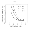
- the temperature -characteristic of the DSM liquid crystal element with respect to the threshold voltage thereof is such as graphically shown in Fig. 1 with the frequency used as a parameter.
- the DSM liquid crystal element employed in the experiment was composed of nematic liquid crystal DNM-4 (made by Dai Nippon Paint Co., Ltd.), and its substrate was processed with parallel orientation at an interval of 10 microns.
- DNM-4 made by Dai Nippon Paint Co., Ltd.
- its threshold voltage increases in accordance with temperature fall.
- the graph further shows that the trend of increase of the threshold voltage induced with temperature fall appears to be more conspicuous with rise of the driving frequency and also that, in case the temperature is maintained constant, the threshold voltage becomes higher as the driving frequency rises.
- the primary object of the present invention resides in providing an improved apparatus which is so designed as to increase a driving voltage for a liquid crystal element in accordance with fall of the element temperature while minimizing a voltage loss during generation of the driving voltage and is still capable of ensuring stable driving of the element despite any variation occurring in a battery voltage applied as a driving input.
- a booster circuit is employed in the present invention to increase the battery voltage.
- the booster circuit is of a feedback control type which receives an input control voltage obtained through division of the aforesaid output voltage and executes boosting to maintain the control voltage constant.
- a voltage divider circuit for dividing the output voltage is composed of a thermistor as a component to sense the temperature of the liquid crystal element, so as to increase the output voltage in conformity with fall of the element temperature.
- Another object of the invention is to provide a liquid crystal element driving apparatus capable of further decreasing the driving voltage in a low temperature region.
- the circuit configuration is so contrived that the frequency of the element driving voltage is lowered sequentially with temperature fall.
- This embodiment is designed to function as a driving apparatus for a glare prevention type reflex mirror equipped with a DSM liquid crystal element on its front.
- a glare preventive operation is performed by applying a voltage to the liquid crystal element to generate a dynamic scattering mode therein and scattering the light with a liquid crystal layer to reduce the reflectivity of the mirror.
- Desired prevention of glare is achieved by the application of a voltage to the DSM liquid crystal when the intensity of the light sensed by a photoelectric transducer element has exceeded a predetermined level.
- a variety of inventions have already been developed with regard to the fundamental structure of such glare preventive reflex mirror as disclosed in, for example, Japanese Patent Publication No. 48-35334.
- FIG. 2 In the electric circuit diagram of Fig. 2 for driving a liquid crystal element, there are shown an automotive battery 1 and a light switch 2. Merely when the light switch 2 is turned on or during nighttime running of an automobile, a voltage is applied to each circuit in the apparatus to perform the above-described glare preventive operation.
- a booster circuit 3 serves to increase an input voltage from the automotive battery 1 up to a level required for driving a liquid crystal element 8.
- a voltage divider 4 includes a thermistor 41 to sense the temperature of the liquid crystal element 8 and functions to divide the output voltage Vl of the booster circuit 3 in cooperation with resistors Rl and R2, thereby producing a control voltage V2 which is outputted to the booster circuit 3.
- the thermistor 41 is attached to a glare preventive reflex mirror so as to sense the temperature of the liquid crystal element 8.
- the resistance of the thermistor 41 has a negative temperature coefficient. Therefore, when temperature fall is sensed by the thermistor 41, its resistance increases to eventually lower the control voltage V2.
- Fig. 3 shows detailed configurations of such booster circuit 3 and voltage divider circuit 4.
- the booster circuit 3 comprises a switching regulator 31 (integrated circuit TL479CN made by Texas Instruments Inc.), which is actuated by the voltage received from the automotive battery 1 via the light switch 2.
- the booster circuit 3 performs its operation by utilizing an electromotive force generated when interrupting the current that flows in a coil L1.
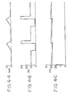
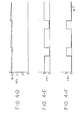
- Fig. 4 shows the waveforms of signals produced in the individual components of the electric circuits.
- the current flowing in the coil Ll is reduced and consequently an electromotive force is generated in proportion to the current reduction rate and the inductance of the coil Ll, so that the collector voltage of the transistor TR3 becomes such as shown in Fig. 4-B.
- the electromotive force thus generated serves to charge a capacitor C2 via a diode D2.
- the voltage retained in the capacitor C2 is released therefrom as an output voltage Vl (shown in Fig. 4-C), which is than divided by a voltage divider circuit 4 consisting of resistors Rl, R2 and a thermistor 41. And the divided voltage is outputted as a control voltage V2 (shown in Fig. 4-B) to the switching regulator 31.
- a comparator 31a compares the control voltage V2 with a reference voltage Vr and, in case the former is lower than the latter, its output (shown in Fig. 4-E) is inverted to a low level. Subsequently, in response to the low-level output voltage thus obtained, an oscillator circuit produces a pulse output (shown in Fig. 4-F) of a fixed duration determined by the capacitor C3. The transistor TR3 is turned on by this pulse output to perform its aforesaid boosting action. That is, when the control voltage V2 becomes lower than the reference voltage Vr, the booster circuit 3 functions to increase the control voltage V2 beyond the reference voltage Vr, thereby changing the output voltage V1 to the vicinity of the reference voltage Vr.
- the switching regulator 31 a current limiter 31c is provided for protection of the circuit from any abnormal current.
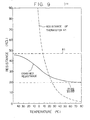
- Fig. 5 graphically shows the resistance characteristic of the thermistor 41 relative to temperature and also the combined resistance characteristic of the thermistor 41 and the resistor Rl relative to temperature.
- the combined resistance value corresponds to the output voltage Vl and increases nonlinearly in accordance with temperature fall.
- the combined resistance is limited to a fixed value by the action of the resistor Rl, thereby preventing any abnormally high resistance value that may otherwise be caused due to the sole existence of the thermistor 41.
- an oscillator circuit 6 produces an oscillation output V3 for applying an AC voltage to the liquid crystal element 8.
- the oscillator circuit 6 employed in this embodiment is of a pulse oscillation type which consists of inverters 61, 62 and 63 composed of C-MOS elements.
- the oscillation frequency of this circuit is determined by a time constant depending on the values of the resistor R3 and the capacitor Cl.
- a thermistor 5 is connected in parallel with two ends of the resistor R3 and functions as a sensor to detect the temperature of the liquid crystal element 8 as the aforesaid thermistor 41.
- the combined resistance of the thermistor 5 and the resistor R3 increases to consequently lower the oscillation frequency of the oscillator circuit 6. In this manner, the oscillation frequency can be lowered in accordance with temperature fall.
- a driving circuit 7 modulates the output voltage Vl of the booster circuit 3 with the frequency of an oscillation voltage V3 obtained from the oscillator circuit 6 and drives the liquid crystal element 8 by such modulated voltage.
- the driving circuit 7 consists of transistors TR1, TR2 and resistors R4, R5, R6 and R7.
- the output voltage Vl of the booster circuit 3 is applied via resistors R4 and R5 respectively to the collectors of transistors TR1 and TR2.
- the output voltage V3 of the oscillator circuit-6 is applied via a resistor R6 to the base of transistor TRl
- the output voltage V7 of an exclusive OR circuit 91 is applied via a resistor R7 to the base of transistor TR2.
- a glare preventive detector circuit 9 for sensing the intensity of the light incident upon the reflex mirror and producing an output signal to execute a glare preventive action in response to any light intensity above a predetermined level consists of a photodiode Dl for sensing the light intensity, an inverter 92 for inverting a signal representative of the output voltage-V4 of the photodiode Dl, and an exclusive OR circuit 91.
- the liquid crystal element 8 receives the rectangular-wave AC voltage which is equal in frequency to the oscillation voltage V3 of the oscillator circuit 6 and is also equal in amplitude to the output voltage Vl of the booster circuit 3. Consequently, a dynamic scattering mode is generated in the liquid crystal element 8 to exert a glare preventive effect on the reflex mirror due to such dynamic scattering induced in the liquid crystal layer.
- Fig. 6 graphically shows the result of measuring the temperature characteristic of the booster circuit 3 with respect to its output voltage Vl in the above embodiment, wherein the voltage Vl increases in accordance with temperature fall.
- the liquid crystal element is driven by the output of 25 volts at 25°C, and the driving voltage is increased to about 40 volts at -30°C..
- Fig. 7 graphically shows the result of measuring the temperature characteristic of the oscillator circuit 6 with respect to the frequency of its oscillation voltage V3 in the above embodiment, wherein the oscillation frequency is lowered with temperature fall.
- the liquid crystal element is driven by the output of 37 Hz at 25°C, and the driving frequency is lowered to 17 Hz at -30°C.
- a resistor R9 may be connected in series with the thermistor 41 as illustrated in Fig. 8.
- the combined resistance value of the resistors Rl, R9 and the thermistor 41 can be set at the lower limit thereof as R1 R9 / R1 + R9 and is therefore settable also at the lower limit relative to the output voltage of the booster circuit 3.
- the resistor Rl in the voltage divider circuit 4 of Fig. 8 may be replaced with a Zener diode ZD1 as shown in Fig. 10.
- the Zener diode ZD1 employed has a Zener voltage of 50 volts
- the diode ZD1 is substantially in an open state when the output voltage Vl is lower than 50 volts.
- a current comes to flow suddenly to maintain the voltage Vl under 50 volts, thereby ensuring a remarkably sharp voltage characteristic with respect to the temperature of the liquid crystal element 8.
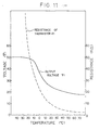
- Fig. 11 graphically shows the temperature characteristic of such voltage divider circuit relative to the output voltage Vl obtained therefrom, wherein a dotted line represents the temperature characteristic of the thermistor 41.
- thermistors are provided in the aforesaid exemplary circuit so as to sense the temperature of the ..element 8.
- a single thermistor is capable of combining the two functions.
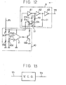
- Fig. 12 is an electric circuit diagram of principal components in such arrangement, wherein a resistor R10 and a photocoupler 51 are provided to change the oscillation frequency of the oscillator circuit 6, and a discriminator circuit 10 is provided for controlling light emission of an LED 51a in the photocoupler 51.
- the discriminator circuit 10 evaluates the output voltage Vl of the booster circuit 3 and controls light emission of the LED 51a in accordance with the result of such evaluation.
- the output voltage V1 of the booster circuit 3 is divided through resistors R11 and R12 to produce a fractional voltage V10, which is subsequently compared with the voltage Vll of a Zener diode ZD2 by a comparator 11.
- the output of the comparator 11 is turned to a low level to switch off the transistor TR4.
- no current comes to flow in the LED 51a of the photocoupler 51, so that the LED 51a is rendered dark to increase the resistance of a photoconductive element 51b. Consequently, the combined resistance of the photoconductive element 51b and the resistor R3 becomes greater to lower the oscillation frequency of the oscillator circuit 6 as a result.
- the oscillator circuit 6 may be constituted of a voltage controlled oscillator (V.C.O.) whose oscillation frequency varies in accordance with the output voltage V1.
- V.C.O. voltage controlled oscillator
- thermistor 41 of another type whose resistance value has a positive temperature coefficient to form a circuit of the configuration shown in Fig. 14.
- resistor R9 used for the thermistor 41 in the foregoing examples of Figs. 10 and 14 may be omitted depending on the temperature characteristic of the thermistor 41 with respect to its resistance value.
Landscapes
- Physics & Mathematics (AREA)
- Chemical & Material Sciences (AREA)
- Crystallography & Structural Chemistry (AREA)
- Nonlinear Science (AREA)
- Engineering & Computer Science (AREA)
- Mathematical Physics (AREA)
- General Physics & Mathematics (AREA)
- Optics & Photonics (AREA)
- Multimedia (AREA)
- Mechanical Engineering (AREA)
- Liquid Crystal (AREA)
- Liquid Crystal Display Device Control (AREA)
Applications Claiming Priority (2)
| Application Number | Priority Date | Filing Date | Title |
|---|---|---|---|
| JP213624/83 | 1983-11-14 | ||
| JP58213624A JPS60104925A (ja) | 1983-11-14 | 1983-11-14 | 液晶素子駆動装置 |
Publications (1)
| Publication Number | Publication Date |
|---|---|
| EP0144828A1 true EP0144828A1 (fr) | 1985-06-19 |
Family
ID=16642242
Family Applications (1)
| Application Number | Title | Priority Date | Filing Date |
|---|---|---|---|
| EP84113754A Ceased EP0144828A1 (fr) | 1983-11-14 | 1984-11-14 | Dispositif de commande d'un élément à cristal liquide |
Country Status (4)
| Country | Link |
|---|---|
| US (1) | US4687956A (fr) |
| EP (1) | EP0144828A1 (fr) |
| JP (1) | JPS60104925A (fr) |
| WO (1) | WO1985002273A1 (fr) |
Cited By (5)
| Publication number | Priority date | Publication date | Assignee | Title |
|---|---|---|---|---|
| FR2673005A1 (fr) * | 1991-02-18 | 1992-08-21 | Asulab Sa | Dispositif optique commandable en frequence. |
| FR2673027A1 (fr) * | 1991-02-20 | 1992-08-21 | Asahi Optical Co Ltd | Dispositif d'affichage a cristal liquide. |
| EP0499878A1 (fr) * | 1991-02-13 | 1992-08-26 | Asulab S.A. | Dispositif optique commandable en fréquence |
| US5267067A (en) * | 1991-02-13 | 1993-11-30 | Asulab S.A. | Frequency controllable optical device |
| DE3927494B4 (de) * | 1989-08-21 | 2006-08-17 | Siemens Ag | Schaltungsanordnung zur Erzeugung einer Steuerspannung für Segmente einer LCD-Anzeige |
Families Citing this family (36)
| Publication number | Priority date | Publication date | Assignee | Title |
|---|---|---|---|---|
| JPS62102231A (ja) * | 1985-10-29 | 1987-05-12 | Casio Comput Co Ltd | 液晶光シャッタの温度制御装置 |
| JPS62126384A (ja) * | 1985-11-27 | 1987-06-08 | Hitachi Ltd | 光学的物体検知装置 |
| US5686835A (en) * | 1989-01-18 | 1997-11-11 | Nippondenso Co., Ltd | Physical quantity detection device for converting a physical quantity into a corresponding time interval |
| EP0379180B1 (fr) * | 1989-01-18 | 1996-11-20 | Nippondenso Co., Ltd. | Dispositif à détection magnétique et dispositif à détection d'une quantité physique l'utilisant |
| JP2868266B2 (ja) * | 1990-01-25 | 1999-03-10 | 株式会社日本自動車部品総合研究所 | 信号位相差検出回路及び信号位相差検出方法 |
| JP2941987B2 (ja) * | 1990-04-09 | 1999-08-30 | キヤノン株式会社 | 液晶表示装置およびその駆動方法 |
| US5563624A (en) * | 1990-06-18 | 1996-10-08 | Seiko Epson Corporation | Flat display device and display body driving device |
| JP3123077B2 (ja) | 1990-06-18 | 2001-01-09 | セイコーエプソン株式会社 | フラット表示装置及び表示体駆動装置 |
| US5164849A (en) * | 1990-10-05 | 1992-11-17 | Allied-Signal Inc. | Liquid crystal display with a fast warm up |
| US5414441A (en) * | 1991-01-11 | 1995-05-09 | Ncr Corporation | Temperature compensation apparatus for liquid crystal display |
| JPH076137U (ja) * | 1993-06-29 | 1995-01-27 | 武智 ツヤ | 茶托兼容器 |
| JP2899199B2 (ja) * | 1993-12-27 | 1999-06-02 | アルプス電気株式会社 | 表示装置における濃度制御装置 |
| US5936604A (en) * | 1994-04-21 | 1999-08-10 | Casio Computer Co., Ltd. | Color liquid crystal display apparatus and method for driving the same |
| GB2288671B (en) * | 1994-04-22 | 1998-04-01 | Delco Electronic Overseas Corp | Liquid crystal display circuit and regulated power supply therefor |
| DE19510049A1 (de) * | 1995-03-20 | 1996-10-02 | Siemens Ag | Schaltung zur Erzeugung einer einstellbaren Ausgangsgleichspannung mit einem über einer Eingangsspannung liegenden Wert, insbesondere zur Verwendung bei der Bereitstellung von Kontrastspannungen für Flüssigkristallanzeigen |
| JP2861879B2 (ja) * | 1995-08-25 | 1999-02-24 | 日本電気株式会社 | 電池パック |
| JP2616496B2 (ja) * | 1995-09-11 | 1997-06-04 | セイコーエプソン株式会社 | 液晶素子の駆動方法 |
| US5936603A (en) * | 1996-01-29 | 1999-08-10 | Delco Electronics Corporation | Liquid crystal display with temperature compensated voltage |
| JP3442581B2 (ja) * | 1996-08-06 | 2003-09-02 | 株式会社ヒューネット | ネマティック液晶の駆動方法 |
| JP3572473B2 (ja) | 1997-01-30 | 2004-10-06 | 株式会社ルネサステクノロジ | 液晶表示制御装置 |
| JP3449898B2 (ja) * | 1997-10-16 | 2003-09-22 | 富士通株式会社 | 発光素子駆動回路 |
| JPH11296150A (ja) | 1998-04-10 | 1999-10-29 | Masaya Okita | 液晶の高速駆動方法 |
| JP2000221468A (ja) * | 1999-01-29 | 2000-08-11 | Citizen Watch Co Ltd | 液晶駆動装置 |
| JP3840856B2 (ja) * | 1999-11-10 | 2006-11-01 | セイコーエプソン株式会社 | 液晶パネルの駆動方法、液晶装置および電子機器 |
| JP2001242836A (ja) * | 2000-02-29 | 2001-09-07 | Matsushita Electric Ind Co Ltd | 液晶表示装置 |
| JP2001318627A (ja) * | 2000-02-29 | 2001-11-16 | Semiconductor Energy Lab Co Ltd | 発光装置 |
| GB0205860D0 (en) * | 2002-03-13 | 2002-04-24 | Koninkl Philips Electronics Nv | Battery operated device with display |
| DE102004014672A1 (de) * | 2004-03-25 | 2005-10-13 | Robert Bosch Gmbh | Anzeigeeinheit und Verfahren zur Anzeige |
| US20070103412A1 (en) * | 2005-11-09 | 2007-05-10 | Pao-Yun Tang | Liquid crystal display having a voltage divider with a thermistor |
| JP4805701B2 (ja) * | 2006-03-17 | 2011-11-02 | シチズンホールディングス株式会社 | 液晶装置 |
| JP5081495B2 (ja) * | 2007-05-02 | 2012-11-28 | 三洋電機株式会社 | 画像表示装置 |
| KR101451572B1 (ko) * | 2007-06-11 | 2014-10-24 | 엘지디스플레이 주식회사 | 액정 표시 장치 및 그 구동방법 |
| KR101472076B1 (ko) * | 2008-08-12 | 2014-12-15 | 삼성디스플레이 주식회사 | 액정 표시 장치 |
| US20100214271A1 (en) * | 2009-02-25 | 2010-08-26 | Seiko Epson Corporation | Liquid crystal device, temperature detection method, and electronic apparatus |
| JP6122111B2 (ja) | 2012-06-28 | 2017-04-26 | ダウ グローバル テクノロジーズ エルエルシー | 多層マイクロキャピラリーフィルムの製造システム、方法、および装置 |
| CN106104993B (zh) * | 2014-05-30 | 2019-05-10 | 三菱电机株式会社 | 电力用半导体元件的驱动电路 |
Citations (4)
| Publication number | Priority date | Publication date | Assignee | Title |
|---|---|---|---|---|
| US4037931A (en) * | 1974-05-02 | 1977-07-26 | Kabushiki Kaisha Suwa Seikosha | Liquid crystal display cell driving circuit |
| DE2327091B2 (de) * | 1972-05-30 | 1978-03-30 | Matsushita Electric Industrial Co., Ltd., Kadoma, Osaka (Japan) | Flüssigkristallanzeigesystem |
| DE3024530A1 (de) * | 1980-06-28 | 1982-01-28 | Eurosil GmbH, 8000 München | Fluessigkristall-steuerspannungsschaltung |
| US4417785A (en) * | 1977-12-27 | 1983-11-29 | Kabushiki Kaisha Suwa Seikosha | Liquid crystal display with negative timing signal and dielectric inversion |
Family Cites Families (9)
| Publication number | Priority date | Publication date | Assignee | Title |
|---|---|---|---|---|
| JPS4835384B1 (fr) * | 1969-08-30 | 1973-10-27 | ||
| US3614210A (en) * | 1969-11-06 | 1971-10-19 | Rca Corp | Liquid crystal day/night mirror |
| JPS4835384A (fr) * | 1971-08-13 | 1973-05-24 | ||
| US3862798A (en) * | 1973-11-19 | 1975-01-28 | Charles L Hopkins | Automatic rear view mirror adjuster |
| JPS5093160A (fr) * | 1973-12-18 | 1975-07-25 | ||
| JPS50106597A (fr) * | 1974-01-23 | 1975-08-22 | ||
| JPS5143095A (ja) * | 1974-10-09 | 1976-04-13 | Sharp Kk | Ekishokudosochi |
| IT1117275B (it) * | 1977-02-25 | 1986-02-17 | Remo Bedini | Metodo e dispositivo automatico per l attenzione dei fenomeni di abbagliamento in luce riflessa |
| US4390874A (en) * | 1981-01-09 | 1983-06-28 | Texas Instruments Incorporated | Liquid crystal display system having improved temperature compensation |
-
1983
- 1983-11-14 JP JP58213624A patent/JPS60104925A/ja active Pending
- 1983-12-13 WO PCT/JP1983/000435 patent/WO1985002273A1/fr not_active Ceased
-
1984
- 1984-11-09 US US06/670,015 patent/US4687956A/en not_active Expired - Fee Related
- 1984-11-14 EP EP84113754A patent/EP0144828A1/fr not_active Ceased
Patent Citations (4)
| Publication number | Priority date | Publication date | Assignee | Title |
|---|---|---|---|---|
| DE2327091B2 (de) * | 1972-05-30 | 1978-03-30 | Matsushita Electric Industrial Co., Ltd., Kadoma, Osaka (Japan) | Flüssigkristallanzeigesystem |
| US4037931A (en) * | 1974-05-02 | 1977-07-26 | Kabushiki Kaisha Suwa Seikosha | Liquid crystal display cell driving circuit |
| US4417785A (en) * | 1977-12-27 | 1983-11-29 | Kabushiki Kaisha Suwa Seikosha | Liquid crystal display with negative timing signal and dielectric inversion |
| DE3024530A1 (de) * | 1980-06-28 | 1982-01-28 | Eurosil GmbH, 8000 München | Fluessigkristall-steuerspannungsschaltung |
Cited By (6)
| Publication number | Priority date | Publication date | Assignee | Title |
|---|---|---|---|---|
| DE3927494B4 (de) * | 1989-08-21 | 2006-08-17 | Siemens Ag | Schaltungsanordnung zur Erzeugung einer Steuerspannung für Segmente einer LCD-Anzeige |
| EP0499878A1 (fr) * | 1991-02-13 | 1992-08-26 | Asulab S.A. | Dispositif optique commandable en fréquence |
| US5267067A (en) * | 1991-02-13 | 1993-11-30 | Asulab S.A. | Frequency controllable optical device |
| FR2673005A1 (fr) * | 1991-02-18 | 1992-08-21 | Asulab Sa | Dispositif optique commandable en frequence. |
| FR2673027A1 (fr) * | 1991-02-20 | 1992-08-21 | Asahi Optical Co Ltd | Dispositif d'affichage a cristal liquide. |
| GB2254709A (en) * | 1991-02-20 | 1992-10-14 | Asahi Optical Co Ltd | Liquid crystal display device. |
Also Published As
| Publication number | Publication date |
|---|---|
| JPS60104925A (ja) | 1985-06-10 |
| WO1985002273A1 (fr) | 1985-05-23 |
| US4687956A (en) | 1987-08-18 |
Similar Documents
| Publication | Publication Date | Title |
|---|---|---|
| US4687956A (en) | Liquid crystal element driving apparatus | |
| US4429236A (en) | Apparatus for generating pulses upon decreases in supply voltage | |
| US4820933A (en) | Control circuit for liquid crystal rear-vision mirror | |
| KR910006817A (ko) | 교류기의 출력 전력 제어용 조절기 | |
| KR880001722B1 (ko) | 발진기 이득제어가 있는 시계회로 | |
| GB2333378A (en) | PWM control circuit for a DC brushless fan | |
| US8270138B2 (en) | Power supply controller and threshold adjustment method thereof | |
| US4236187A (en) | Power supply voltage stabilizer | |
| KR0160440B1 (ko) | 자체 발진 블로킹 발진기형 스위칭 파워팩 회로 | |
| GB1519225A (en) | Lamp power supply using a dc regulator and a commutator | |
| EP0483082A2 (fr) | Circuit pour contrôler une lampe à décharge sur un véhicule | |
| US4388587A (en) | Fixed frequency voltage regulator | |
| US4736091A (en) | Integral sensor controller for an electrical heater | |
| EP0068405B1 (fr) | Circuit de traitement de signaux impulsionnels comportant un circuit de protection contre les surintensités de courant | |
| US4388586A (en) | Fixed frequency voltage regulator | |
| JPH07202584A (ja) | 低電圧誤動作防止機能付過熱保護回路 | |
| US4328537A (en) | Circuit arrangement for limiting and regulating the collector current of the control element transistor of a switching network component | |
| US4011002A (en) | Electronic device for detecting the energized state of a liquid crystal display cell | |
| US3969665A (en) | Automatic control circuit for battery charging systems | |
| EP1131669B1 (fr) | Procede et circuit electronique d'excitation pour l'element de commutation electro-optique d'un afficheur a cristaux liquides | |
| US3550006A (en) | Temperature control for crystal oscillator and modulation circuit of a radio transmitter | |
| US11456590B2 (en) | Short circuit detection module and short circuit detection method applied thereto | |
| JPH02284072A (ja) | 無線周波エネルギー検出回路 | |
| EP0081891B1 (fr) | Régulateur de tension à fréquence constante | |
| JPS61117525A (ja) | 液晶素子駆動装置 |
Legal Events
| Date | Code | Title | Description |
|---|---|---|---|
| PUAI | Public reference made under article 153(3) epc to a published international application that has entered the european phase |
Free format text: ORIGINAL CODE: 0009012 |
|
| AK | Designated contracting states |
Designated state(s): DE FR GB |
|
| 17P | Request for examination filed |
Effective date: 19850805 |
|
| 17Q | First examination report despatched |
Effective date: 19861127 |
|
| STAA | Information on the status of an ep patent application or granted ep patent |
Free format text: STATUS: THE APPLICATION HAS BEEN REFUSED |
|
| 18R | Application refused |
Effective date: 19880731 |
|
| RIN1 | Information on inventor provided before grant (corrected) |
Inventor name: OHMI, SHINYA Inventor name: HARA, KUNIHIKO Inventor name: ITOH, HIROSHI Inventor name: SUZUKI, YASUTOSHI Inventor name: FUKADA, TSUYOSHI |