EP0147626A2 - Dispositif semi-conducteur comprenant des transistors bipolaire et MOS et procédé pour sa fabrication - Google Patents
Dispositif semi-conducteur comprenant des transistors bipolaire et MOS et procédé pour sa fabrication Download PDFInfo
- Publication number
- EP0147626A2 EP0147626A2 EP84114151A EP84114151A EP0147626A2 EP 0147626 A2 EP0147626 A2 EP 0147626A2 EP 84114151 A EP84114151 A EP 84114151A EP 84114151 A EP84114151 A EP 84114151A EP 0147626 A2 EP0147626 A2 EP 0147626A2
- Authority
- EP
- European Patent Office
- Prior art keywords
- semiconductor
- layer
- silicon
- layers
- semiconductor device
- Prior art date
- Legal status (The legal status is an assumption and is not a legal conclusion. Google has not performed a legal analysis and makes no representation as to the accuracy of the status listed.)
- Withdrawn
Links
Images


Classifications
-
- H—ELECTRICITY
- H10—SEMICONDUCTOR DEVICES; ELECTRIC SOLID-STATE DEVICES NOT OTHERWISE PROVIDED FOR
- H10P—GENERIC PROCESSES OR APPARATUS FOR THE MANUFACTURE OR TREATMENT OF DEVICES COVERED BY CLASS H10
- H10P14/00—Formation of materials, e.g. in the shape of layers or pillars
- H10P14/20—Formation of materials, e.g. in the shape of layers or pillars of semiconductor materials
- H10P14/29—Formation of materials, e.g. in the shape of layers or pillars of semiconductor materials characterised by the substrates
- H10P14/2926—Crystal orientations
-
- H—ELECTRICITY
- H10—SEMICONDUCTOR DEVICES; ELECTRIC SOLID-STATE DEVICES NOT OTHERWISE PROVIDED FOR
- H10P—GENERIC PROCESSES OR APPARATUS FOR THE MANUFACTURE OR TREATMENT OF DEVICES COVERED BY CLASS H10
- H10P14/00—Formation of materials, e.g. in the shape of layers or pillars
- H10P14/20—Formation of materials, e.g. in the shape of layers or pillars of semiconductor materials
- H10P14/27—Formation of materials, e.g. in the shape of layers or pillars of semiconductor materials using selective deposition, e.g. simultaneous growth of monocrystalline and non-monocrystalline semiconductor materials
-
- H—ELECTRICITY
- H10—SEMICONDUCTOR DEVICES; ELECTRIC SOLID-STATE DEVICES NOT OTHERWISE PROVIDED FOR
- H10D—INORGANIC ELECTRIC SEMICONDUCTOR DEVICES
- H10D84/00—Integrated devices formed in or on semiconductor substrates that comprise only semiconducting layers, e.g. on Si wafers or on GaAs-on-Si wafers
- H10D84/01—Manufacture or treatment
- H10D84/0107—Integrating at least one component covered by H10D12/00 or H10D30/00 with at least one component covered by H10D8/00, H10D10/00 or H10D18/00, e.g. integrating IGFETs with BJTs
- H10D84/0109—Integrating at least one component covered by H10D12/00 or H10D30/00 with at least one component covered by H10D8/00, H10D10/00 or H10D18/00, e.g. integrating IGFETs with BJTs the at least one component covered by H10D12/00 or H10D30/00 being a MOS device
-
- H—ELECTRICITY
- H10—SEMICONDUCTOR DEVICES; ELECTRIC SOLID-STATE DEVICES NOT OTHERWISE PROVIDED FOR
- H10D—INORGANIC ELECTRIC SEMICONDUCTOR DEVICES
- H10D84/00—Integrated devices formed in or on semiconductor substrates that comprise only semiconducting layers, e.g. on Si wafers or on GaAs-on-Si wafers
- H10D84/01—Manufacture or treatment
- H10D84/0123—Integrating together multiple components covered by H10D12/00 or H10D30/00, e.g. integrating multiple IGBTs
- H10D84/0126—Integrating together multiple components covered by H10D12/00 or H10D30/00, e.g. integrating multiple IGBTs the components including insulated gates, e.g. IGFETs
- H10D84/0165—Integrating together multiple components covered by H10D12/00 or H10D30/00, e.g. integrating multiple IGBTs the components including insulated gates, e.g. IGFETs the components including complementary IGFETs, e.g. CMOS devices
-
- H—ELECTRICITY
- H10—SEMICONDUCTOR DEVICES; ELECTRIC SOLID-STATE DEVICES NOT OTHERWISE PROVIDED FOR
- H10D—INORGANIC ELECTRIC SEMICONDUCTOR DEVICES
- H10D84/00—Integrated devices formed in or on semiconductor substrates that comprise only semiconducting layers, e.g. on Si wafers or on GaAs-on-Si wafers
- H10D84/01—Manufacture or treatment
- H10D84/02—Manufacture or treatment characterised by using material-based technologies
- H10D84/03—Manufacture or treatment characterised by using material-based technologies using Group IV technology, e.g. silicon technology or silicon-carbide [SiC] technology
- H10D84/038—Manufacture or treatment characterised by using material-based technologies using Group IV technology, e.g. silicon technology or silicon-carbide [SiC] technology using silicon technology, e.g. SiGe
-
- H—ELECTRICITY
- H10—SEMICONDUCTOR DEVICES; ELECTRIC SOLID-STATE DEVICES NOT OTHERWISE PROVIDED FOR
- H10D—INORGANIC ELECTRIC SEMICONDUCTOR DEVICES
- H10D84/00—Integrated devices formed in or on semiconductor substrates that comprise only semiconducting layers, e.g. on Si wafers or on GaAs-on-Si wafers
- H10D84/40—Integrated devices formed in or on semiconductor substrates that comprise only semiconducting layers, e.g. on Si wafers or on GaAs-on-Si wafers characterised by the integration of at least one component covered by groups H10D12/00 or H10D30/00 with at least one component covered by groups H10D10/00 or H10D18/00, e.g. integration of IGFETs with BJTs
- H10D84/401—Combinations of FETs or IGBTs with BJTs
-
- H—ELECTRICITY
- H10—SEMICONDUCTOR DEVICES; ELECTRIC SOLID-STATE DEVICES NOT OTHERWISE PROVIDED FOR
- H10P—GENERIC PROCESSES OR APPARATUS FOR THE MANUFACTURE OR TREATMENT OF DEVICES COVERED BY CLASS H10
- H10P14/00—Formation of materials, e.g. in the shape of layers or pillars
- H10P14/20—Formation of materials, e.g. in the shape of layers or pillars of semiconductor materials
- H10P14/29—Formation of materials, e.g. in the shape of layers or pillars of semiconductor materials characterised by the substrates
- H10P14/2901—Materials
- H10P14/2902—Materials being Group IVA materials
- H10P14/2905—Silicon, silicon germanium or germanium
-
- H—ELECTRICITY
- H10—SEMICONDUCTOR DEVICES; ELECTRIC SOLID-STATE DEVICES NOT OTHERWISE PROVIDED FOR
- H10P—GENERIC PROCESSES OR APPARATUS FOR THE MANUFACTURE OR TREATMENT OF DEVICES COVERED BY CLASS H10
- H10P14/00—Formation of materials, e.g. in the shape of layers or pillars
- H10P14/20—Formation of materials, e.g. in the shape of layers or pillars of semiconductor materials
- H10P14/32—Formation of materials, e.g. in the shape of layers or pillars of semiconductor materials characterised by intermediate layers between substrates and deposited layers
- H10P14/3202—Materials thereof
- H10P14/3238—Materials thereof being insulating materials
-
- H—ELECTRICITY
- H10—SEMICONDUCTOR DEVICES; ELECTRIC SOLID-STATE DEVICES NOT OTHERWISE PROVIDED FOR
- H10P—GENERIC PROCESSES OR APPARATUS FOR THE MANUFACTURE OR TREATMENT OF DEVICES COVERED BY CLASS H10
- H10P14/00—Formation of materials, e.g. in the shape of layers or pillars
- H10P14/20—Formation of materials, e.g. in the shape of layers or pillars of semiconductor materials
- H10P14/32—Formation of materials, e.g. in the shape of layers or pillars of semiconductor materials characterised by intermediate layers between substrates and deposited layers
- H10P14/3242—Structure
- H10P14/3244—Layer structure
- H10P14/3248—Layer structure consisting of two layers
-
- H—ELECTRICITY
- H10—SEMICONDUCTOR DEVICES; ELECTRIC SOLID-STATE DEVICES NOT OTHERWISE PROVIDED FOR
- H10P—GENERIC PROCESSES OR APPARATUS FOR THE MANUFACTURE OR TREATMENT OF DEVICES COVERED BY CLASS H10
- H10P14/00—Formation of materials, e.g. in the shape of layers or pillars
- H10P14/20—Formation of materials, e.g. in the shape of layers or pillars of semiconductor materials
- H10P14/34—Deposited materials, e.g. layers
- H10P14/3402—Deposited materials, e.g. layers characterised by the chemical composition
- H10P14/3404—Deposited materials, e.g. layers characterised by the chemical composition being Group IVA materials
- H10P14/3411—Silicon, silicon germanium or germanium
-
- H—ELECTRICITY
- H10—SEMICONDUCTOR DEVICES; ELECTRIC SOLID-STATE DEVICES NOT OTHERWISE PROVIDED FOR
- H10P—GENERIC PROCESSES OR APPARATUS FOR THE MANUFACTURE OR TREATMENT OF DEVICES COVERED BY CLASS H10
- H10P14/00—Formation of materials, e.g. in the shape of layers or pillars
- H10P14/20—Formation of materials, e.g. in the shape of layers or pillars of semiconductor materials
- H10P14/34—Deposited materials, e.g. layers
- H10P14/3451—Structure
- H10P14/3452—Microstructure
- H10P14/3458—Monocrystalline
-
- H—ELECTRICITY
- H10—SEMICONDUCTOR DEVICES; ELECTRIC SOLID-STATE DEVICES NOT OTHERWISE PROVIDED FOR
- H10P—GENERIC PROCESSES OR APPARATUS FOR THE MANUFACTURE OR TREATMENT OF DEVICES COVERED BY CLASS H10
- H10P14/00—Formation of materials, e.g. in the shape of layers or pillars
- H10P14/20—Formation of materials, e.g. in the shape of layers or pillars of semiconductor materials
- H10P14/38—Formation of materials, e.g. in the shape of layers or pillars of semiconductor materials characterised by treatments done after the formation of the materials
- H10P14/3802—Crystallisation or recrystallisation of non-monocrystalline semiconductor materials, e.g. regrowth
- H10P14/3808—Crystallisation or recrystallisation of non-monocrystalline semiconductor materials, e.g. regrowth using laser beams
-
- H—ELECTRICITY
- H10—SEMICONDUCTOR DEVICES; ELECTRIC SOLID-STATE DEVICES NOT OTHERWISE PROVIDED FOR
- H10P—GENERIC PROCESSES OR APPARATUS FOR THE MANUFACTURE OR TREATMENT OF DEVICES COVERED BY CLASS H10
- H10P90/00—Preparation of wafers not covered by a single main group of this subclass, e.g. wafer reinforcement
- H10P90/19—Preparing inhomogeneous wafers
- H10P90/1904—Preparing vertically inhomogeneous wafers
- H10P90/1906—Preparing SOI wafers
-
- H—ELECTRICITY
- H10—SEMICONDUCTOR DEVICES; ELECTRIC SOLID-STATE DEVICES NOT OTHERWISE PROVIDED FOR
- H10W—GENERIC PACKAGES, INTERCONNECTIONS, CONNECTORS OR OTHER CONSTRUCTIONAL DETAILS OF DEVICES COVERED BY CLASS H10
- H10W10/00—Isolation regions in semiconductor bodies between components of integrated devices
- H10W10/01—Manufacture or treatment
- H10W10/061—Manufacture or treatment using SOI processes together with lateral isolation, e.g. combinations of SOI and shallow trench isolations
-
- H—ELECTRICITY
- H10—SEMICONDUCTOR DEVICES; ELECTRIC SOLID-STATE DEVICES NOT OTHERWISE PROVIDED FOR
- H10W—GENERIC PACKAGES, INTERCONNECTIONS, CONNECTORS OR OTHER CONSTRUCTIONAL DETAILS OF DEVICES COVERED BY CLASS H10
- H10W10/00—Isolation regions in semiconductor bodies between components of integrated devices
- H10W10/10—Isolation regions comprising dielectric materials
- H10W10/181—Semiconductor-on-insulator [SOI] isolation regions, e.g. buried oxide regions of SOI wafers
-
- H—ELECTRICITY
- H10—SEMICONDUCTOR DEVICES; ELECTRIC SOLID-STATE DEVICES NOT OTHERWISE PROVIDED FOR
- H10P—GENERIC PROCESSES OR APPARATUS FOR THE MANUFACTURE OR TREATMENT OF DEVICES COVERED BY CLASS H10
- H10P90/00—Preparation of wafers not covered by a single main group of this subclass, e.g. wafer reinforcement
- H10P90/19—Preparing inhomogeneous wafers
- H10P90/1904—Preparing vertically inhomogeneous wafers
- H10P90/1906—Preparing SOI wafers
- H10P90/1912—Preparing SOI wafers using selective deposition, e.g. epitaxial lateral overgrowth [ELO] or selective deposition of single crystal silicon
-
- H—ELECTRICITY
- H10—SEMICONDUCTOR DEVICES; ELECTRIC SOLID-STATE DEVICES NOT OTHERWISE PROVIDED FOR
- H10W—GENERIC PACKAGES, INTERCONNECTIONS, CONNECTORS OR OTHER CONSTRUCTIONAL DETAILS OF DEVICES COVERED BY CLASS H10
- H10W10/00—Isolation regions in semiconductor bodies between components of integrated devices
- H10W10/01—Manufacture or treatment
- H10W10/011—Manufacture or treatment of isolation regions comprising dielectric materials
- H10W10/012—Manufacture or treatment of isolation regions comprising dielectric materials using local oxidation of silicon [LOCOS]
-
- H—ELECTRICITY
- H10—SEMICONDUCTOR DEVICES; ELECTRIC SOLID-STATE DEVICES NOT OTHERWISE PROVIDED FOR
- H10W—GENERIC PACKAGES, INTERCONNECTIONS, CONNECTORS OR OTHER CONSTRUCTIONAL DETAILS OF DEVICES COVERED BY CLASS H10
- H10W10/00—Isolation regions in semiconductor bodies between components of integrated devices
- H10W10/10—Isolation regions comprising dielectric materials
- H10W10/13—Isolation regions comprising dielectric materials formed using local oxidation of silicon [LOCOS], e.g. sealed interface localised oxidation [SILO] or side-wall mask isolation [SWAMI]
Definitions
- the present invention relates to a semiconductor device and a method of fabricating the same.
- the present invention relates to a semiconductor integrated circuit device in which a bipolar transistor and a plurality of metal oxide semiconductor field effect transistor or a complementary metal oxide semiconductor field effect transistor (hereinafter referred to as "CMOS transistor") are formed on the same semiconductor substrate without producing any interaction between the transistors.
- CMOS transistor complementary metal oxide semiconductor field effect transistor
- An object of the present invention is to increase the number of elements per chip in such a manner that semiconductor element regions on a semiconductor substrate are isolated from each other by a groove.
- Another object of the present invention is to provide a method of forming a bipolar transistor and a CMOS transistor on a semiconductor substrate at a high packing density without producing any parasitic effect between semiconductor elements, and a semiconductor device fabricated by the above method.
- a semiconductor layer which is epitaxally grown on a substrate is divided by an insulating material or air into semiconductor element regions, and the element regions are isolated from each other so as not to produce any parasitic effect therebetween.
- Figs. la through lg, Fig. 2, Figs. 3a and 3b, Fig. 4 and Figs. 5a through 5d show various embodiments of the present invention.
- a silicon oxide film or layer 2 (namely, SiO 2 layer 2) is formed on a principal surface of a P-type silicon substrate 1 which is parallel to a (100) crystallographic plane, to a thickness of 10 to 50 nm by keeping the silicon substrate 1 at about 1,000°C in the atmosphere of dry oxygen for a period of 10 to 60 min., that is, by the thermal oxidation method.
- Mixed gas of SiH 2 Cl 2 and NH 3 is caused to flow at a temperature of about 770°C and a pressure of 80 Pa for a period of 20 to 100 min., while keeping the flow rates of SiH 2 Cl 2 and NH 3 at 0.03 i/min. and 0.33 l/min., respectively.
- a silicon nitride layer 3 having a thickness of 50 to 200 nm is deposited on the SiO 2 layer 2 by chemical vapor deposition.
- the composition of the silicon nitride layer 3 is such that an atomic ratio of silicon to nitrogen lies in a range from 0.7 to 1.1, and the silicon nitride layer 3 is typically made of Si 3 N 4 .
- the present inventors formed the window 4 in such a manner that the layers 2 and 3 were selectively etched by the sputtering which is carried out for a period of 1 to 3 min. in the atmosphere of CF 4 gas having a pressure of about 50 Pa and kept at a temperature of about 80°C, and consumes a power of 100 W.
- a diffusion source Sb 2 O 3 is heated to about 1,175°C, to be sublimated, and the vaporized Sb is diffused (or driven) from the bottom of the window 4 into the silicon substrate 1, to form a diffusion layer 5.
- the layers 2 and 3 function as a mask.
- the diffusion layer 5 is not always indispensable for a dielectric isolation semiconductor device according to the present invention, but will be effectively used as the buried collector layer of a bipolar transistor formed in a semiconductor region on the diffusion layer 5.
- an epitaxial silicon layer is grown on the silicon substrate 1 including the layers 2, 3 and 5, at a temperature of 900 to 1,000°C by mixed gas of SiCl 4 and H 2 .
- a monocrystalline silicon layer 6 is grown on the buried layer 5, and polysilicon layers 21 and 22 having a depth of 0.3 to 3 ⁇ m are grown on the silicon nitride layer 3.
- the layers 6, 21 and 22 are doped with a small quantity of phosphorus to have the N-type conductivity, that is, phosphorus is doped into these layers at an impurity concentration of 5 x 10 14 to 5 x 1 0 15 c m -3 using phosphine (PH 3 ) gas between 900 to 1000°C.
- phosphine (PH 3 ) gas between 900 to 1000°C.
- an Si0 2 layer 8 is then formed on the layers 6, 21 and 22 to a thickness of 10 to 50 nm, using the same fabricating conditions as in forming the Sio 2 layer 2 on the silicon substrate 1 by the thermal oxidation method, and then a silicon nitride layer 9 is deposited on the Sio 2 layer 8 to a thickness of 50 to 200 nm, using the same fabricating conditions as in forming the silicon nitride layer 3.
- Those portions of the silicon nitride layer 9, under which isolation grooves are to be provided for separating MOS and bipolar-transistors on the substrate 1, are selecting dry-etched off by CF 4 -4% 0 2 plasma over a width of-about-1 ⁇ m or more through the well-known photoresist techniques (Freon is the trade name of CF 4 ). In this ethcing process, the exposed surface of the SiO 2 layer 8 may be slightly etched.
- the substrate 1 treated is placed in the atmosphere of wet oxygen having a temperature of about 1,000°C and a pressure of about 6 K g/cm 2 , for a period of 40 to 120 min., to selectively form a thermal oxidation film 10 having a width of 1 to 3 ⁇ m and a thickness of 1 to 2 um (that is, a thickness capable of reaching the silicon nitride layer 3), on the basis of a difference in permeability to oxygen gas between the silicon nitride layer 9 and SiO 2 layer 8.
- the polysilicon layer 22 is isolated from the semiconductor regions 1 and 6 by the insulators 3 and 10, and is divided by the insulator 10 into layers 22' and 23.
- Each of the semiconductor regions 6, 22' and 23 is surrounded by the insulator 10, as shown in Fig. ld.
- the silicon nitride layer 9 is removed by the well-known wet etching techniques by hot phosphoric acid aqueous solution at about 170°C for 30 min. and then an SiO 2 layer 11 is deposited to a thickness of 0.3 to 2 ⁇ m as shown in Fig. le, by using the thermal decomposition of Si(OC2H5)4.
- the substrate 1 thus treated is placed on a carbon heater 20 which has a substrate-accepting recess 21 (0.1 - 0.5 mm depth) is pre-heated to a temperature of 1,100 to 1,300°C, and the upper side of the substrate 1 is irradiated with laser or infrared light as indicated by an arrow 19, to be rapidly heated.
- the SiO 2 layer 11 prevents the evaporation of silicon from the surfaces of molten silicon layers 6, 32 and 33. Since the bottom of the monocrystalline region 6 is kept in contact with the substrate 1 which is high in thermal conductivity, heat supplied to the region 6 is rapidly conducted to the substrate 1.
- the SiO 2 layer 2 and silicon nitride layer 3 which are relatively low in thermal conductivity, are interposed between the crystalline layers 22' and 23 and the substrate 1.
- heat supplied to the layers 22' and 23 is hard to dissipate.
- the upper side of the substrate 1 can be heated so that the monocrystalline silicon layer 6 is not melted but only the polysilicon layers 22' and 23 are melted. That is, the polysilicon layers 22' and 23 can be transformed into the approximately monocrystallized layers 32 and 33, without giving any adverse effect on the monocrystalline silicon layer 6.
- each of the layers 32 and 33 may be monocrystallized imperfectly, such imperfect monocrystalline portions will not arouse a serious problem when an MOS transistor is formed in each of these layers 32 and 33.
- the Sio 2 layer 11 is then removed by the well-known etching techniques (for example, by the etchant HF and NH 4 F at about 25°C).
- a photoresist film 12 is selectively formed by the well-known photoresist techniques to a thickness of 0.5 to 1.5 pm, as shown in Fig. lf, and boron ions are implanted into the approximately monocrystallized layer 32 with an implant energy of about 60 KeV, to form a P-type silicon layer 32 which is approximately monocrystallized and has an impurity concentration of 0 . 5 to 3 x 10 12 cm -3 . At this time, the N-type silicon layers 6 and 33 are left unchanged. The photoresist film 12 is then removed. Thereafter, as shown in Fig.
- a bipolar transistor, an N-channel MOS transistor, and a P-channel MOS transistor are formed in the N-type monocrystalline silicon layer 6, the P-type approximately-monocrystallized silicon layer 32, and the N-type approximately-monocrystallized silicon layer 33, respectively, through well-known semiconductor techniques.
- the N-channel MOS transistor and P-channel MOS transistor are connected to each other to form a CMOS transistor.
- the Si epitaxial layer having a 0.5 ⁇ m is preferable to provide the narrow width of the SiO 2 layer 10, about 0.5 ⁇ m, and the 0.7 ⁇ m rule is applied to obtain the width L of 13 x 0.7 + 2 x 0.5 ⁇ 10 ⁇ m.
- Fig. lf may be omitted to obtain a second embodiment of the present invention.
- two MOS transistors can be formed by providing two N-channel MOS transistors on the layers 32 and 33.
- One of the MOS transistors may be coupled with the base of the bipolar transistor to form a bi-MOS transistor having a high input impedance.
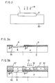
- FIG. 4 A third embodiment of the present invention will be explained, with reference to Fig. 4.
- An N +- silicon substrate 41 having a principal surface paralle to a (100) crystallographic plane and an impurity concentration of 10 19 to 10 21 cm -3 is first prepared. Then, various layers are formed by using fabricating conditions corresponding to the fabricating conditions which have been explained with reference to Figs. la through lg. In Fig. 4, these layers are designated by the same reference numerals as in Fig. la through lg.
- a P-type base region 43 is formed, by the well-known ion implantation method, in the N-type epitaxially-grown layer 6 which is kept in direct contact with the substrate 41, and an N-type emitter region 45 is formed in the P-type base region 43 by the ion implantation method.
- a contact electrode is provided on each of the base region 43 and emitter region 45.
- a collector contact electrode is provided on a principal surface of the substrate 41 opposite to the monocrystalline silicon layer 6.
- a vertical NPN power transistor 48 is obtained which is large in current passing area.
- the power transistor 48 can be driven by an MOS transistor 47 formed in the P-type or N-type approximately-monocrystallized silicon region 32.
- a fourth embodiment of the present invention is different from the above-mentioned third embodiment in that a bipolar transistor is formed in the region 32 to drive the power transistor 48.
- a fifth embodiment of the present invention is different from the third embodiment in that a P-type substrate is used for forming a PNP power transistor in place of the NPN power transistor 48.
- FIG. 3a A sixth embodiment of the present invention will be explained below, with reference to Figs. 3a and 3b.
- the same layers as in Figs. la through lg are designated by the same reference numerals.
- a ring-shaped, highly-doped, P ++ -layer55 is formed in the substrate 1 by the photolithographic techniques and ion implantation method. Thereafter, the substrate 1 is treated in the same manner as having been explained with reference to Figs. lb to lf. The substrate thus obtained is shown in Fig. 3a.
- the ring-shaped buried layer 55 is very effective for electrically isolating the buried collector layer 5 from a plurality of bipolar/CMOS transistors formed in that surface portion of the substrate 1 which is not shown in Figs. 3a and 3b.
- a seventh embodiment of the present invention is shown in which, prior to forming the insulator 10 of Fig. ld, laser heating is carried out.
- a (100) crystallographic plane can be formed in respective surfaces of the regions 22' and 23 as in the principal surface of the substrate 1.
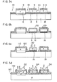
- a ninth embodiment of the present embodiment is shown in Figs. 5a through 5d.
- the substrate 1 is prepared in accordance with the steps shown in Figs. la to lc.
- KOH : H 2 O : IPA (isopropyl alcohol) 1000 g : 2333 ml : 200 ml at about 75°C to a depth reaching the silicon nitride layer 3 by using the silicon nitride layer 9 as a mask, and thus circuit element regions are separated from each other by air in an empty space 101.
- the polysilicon layers 22 and 23 which are left unetched, are approximately monocrystallized by the heat treatment using laser or infrared light. At this time, the monocrystalline silicon layer 6 is not melted.
- the above heat treatment may be carried out between the step shown in Fig. lC and the step shown in Fig. 5a.
- the portion of the silicon nitride layer 3 lying at the bottom of the empty space 101 and the silicon nitride layer 9 on each circuit element region are etched off by the hot H 3 PO 4 -H 2 O at about 170°C for 30 min.. Then., as shown in Fig.
- an Sio 2 layer 110 is deposited on the substrate 1 to a thickness of 0.3 to 2.0 ⁇ m by the thermal decomposition method, and a photoresist film 120 having a thickness of 0.5 to 1.5 ⁇ m is provided on two islands other than a center island.
- the SiO 2 layer 110 on the center island is etched off by using the photoresist film 120 as a mask.
- boron ions are implanted into the approximately monocrystallized silicon layer 32 which is the center island, with an implant energy of about 60 KeV, to form a P-type layer having an impurity concentration of 0 . 5 to 3 x 1 0 12 cm -3 .
- the photoresist film 120 and Si0 2 layer 110 are etched off.
- a phosphosilicate glass film 140 is deposited in the empty regions 101 by the plasma CVD method to a thickness of 0.2 to 1.5 ⁇ m and then a silicon nitride or oxide film 150 is deposited on the phosphosilicate glass film 140 by the plasma CVD method to a thickness of 0.1 to 1.0 pm, as shown in Fig. 5d.
- the deposition of these films 140 and 150 is carried out, while using a photoresist film (not shown) on the three islands as a mask.
- An NPN transistor 152, an N-channel MOS transistor 154 and a P-channel MOS transistor 156 are formed in the silicon layers 6, 32'and 33 forming the three islands, respectively.
- the N-channel MOS transistor 154 and P-channel M OS transistor 156 are connected to each other to form a CMOS transistor.
- narrow dielectric isolation layer can be formed, without producing a parasitic element, in accordance with the invention. Accordingly, the compact or high density integrated circuit having a bipolar and MOS transistors can be presented.
Landscapes
- Metal-Oxide And Bipolar Metal-Oxide Semiconductor Integrated Circuits (AREA)
- Element Separation (AREA)
- Recrystallisation Techniques (AREA)
Applications Claiming Priority (2)
| Application Number | Priority Date | Filing Date | Title |
|---|---|---|---|
| JP58219446A JPS60113455A (ja) | 1983-11-24 | 1983-11-24 | 半導体集積回路装置 |
| JP219446/83 | 1983-11-24 |
Publications (2)
| Publication Number | Publication Date |
|---|---|
| EP0147626A2 true EP0147626A2 (fr) | 1985-07-10 |
| EP0147626A3 EP0147626A3 (fr) | 1987-08-12 |
Family
ID=16735534
Family Applications (1)
| Application Number | Title | Priority Date | Filing Date |
|---|---|---|---|
| EP84114151A Withdrawn EP0147626A3 (fr) | 1983-11-24 | 1984-11-23 | Dispositif semi-conducteur comprenant des transistors bipolaire et MOS et procédé pour sa fabrication |
Country Status (2)
| Country | Link |
|---|---|
| EP (1) | EP0147626A3 (fr) |
| JP (1) | JPS60113455A (fr) |
Cited By (10)
| Publication number | Priority date | Publication date | Assignee | Title |
|---|---|---|---|---|
| US4710794A (en) * | 1985-02-13 | 1987-12-01 | Kabushiki Kaisha Toshiba | Composite semiconductor device |
| EP0364393A3 (fr) * | 1988-10-12 | 1990-06-06 | Nippon Telegraph And Telephone Corporation | Dispositif semi-conducteur de puissance |
| US4948748A (en) * | 1985-09-30 | 1990-08-14 | Kabushiki Kaisha Toshiba | Manufacture of a substrate structure for a composite semiconductor device using wafer bonding and epitaxial refill |
| WO1990009679A1 (fr) * | 1989-02-20 | 1990-08-23 | Fraunhofer-Gesellschaft zur Förderung der angewandten Forschung e.V. | Circuit de puissance a circuit bipolaire ou cmos integre et procede de fabrication de circuits integres |
| US4970174A (en) * | 1987-09-15 | 1990-11-13 | Samsung Electronics Co., Ltd. | Method for making a BiCMOS semiconductor device |
| US4985745A (en) * | 1988-01-05 | 1991-01-15 | Kabushiki Kaisha Toshiba | Substrate structure for composite semiconductor device |
| DE4204004A1 (de) * | 1992-02-12 | 1993-08-19 | Daimler Benz Ag | Verfahren zur herstellung einer halbleiterstruktur mit vertikalen und lateralen halbleiterbauelementen und nach dem verfahren hergestellte halbleiterstruktur |
| US5440166A (en) * | 1991-10-31 | 1995-08-08 | Sgs-Thomson Microelectronics, Inc. | Planarized isolation structure for CMOS devices |
| EP1193752A1 (fr) * | 2000-09-28 | 2002-04-03 | Motorola, Inc. | Méthode de fabrication d'une structure de silicium sur isolant localisée |
| US6559505B1 (en) * | 1999-04-06 | 2003-05-06 | Stmicroelectronics S.R.L. | Power integrated circuit with vertical current flow and related manufacturing process |
Family Cites Families (2)
| Publication number | Priority date | Publication date | Assignee | Title |
|---|---|---|---|---|
| DE1439725A1 (de) * | 1964-09-17 | 1968-11-28 | Telefunken Patent | Verfahren zur Herstellung separierter Halbleiterbereiche mit geringer Nebenschlusskapazitaet in einer mikrominiaturisierten Schaltungsanordnung |
| US4016596A (en) * | 1975-06-19 | 1977-04-05 | International Business Machines Corporation | High performance integrated bipolar and complementary field effect transistors |
-
1983
- 1983-11-24 JP JP58219446A patent/JPS60113455A/ja active Pending
-
1984
- 1984-11-23 EP EP84114151A patent/EP0147626A3/fr not_active Withdrawn
Cited By (13)
| Publication number | Priority date | Publication date | Assignee | Title |
|---|---|---|---|---|
| US4710794A (en) * | 1985-02-13 | 1987-12-01 | Kabushiki Kaisha Toshiba | Composite semiconductor device |
| US4948748A (en) * | 1985-09-30 | 1990-08-14 | Kabushiki Kaisha Toshiba | Manufacture of a substrate structure for a composite semiconductor device using wafer bonding and epitaxial refill |
| US4970174A (en) * | 1987-09-15 | 1990-11-13 | Samsung Electronics Co., Ltd. | Method for making a BiCMOS semiconductor device |
| US4985745A (en) * | 1988-01-05 | 1991-01-15 | Kabushiki Kaisha Toshiba | Substrate structure for composite semiconductor device |
| EP0364393A3 (fr) * | 1988-10-12 | 1990-06-06 | Nippon Telegraph And Telephone Corporation | Dispositif semi-conducteur de puissance |
| WO1990009679A1 (fr) * | 1989-02-20 | 1990-08-23 | Fraunhofer-Gesellschaft zur Förderung der angewandten Forschung e.V. | Circuit de puissance a circuit bipolaire ou cmos integre et procede de fabrication de circuits integres |
| DE3905149A1 (de) * | 1989-02-20 | 1990-08-30 | Fraunhofer Ges Forschung | Leistungsschaltung mit einer integrierten cmos- oder bipolar-schaltung und verfahren zum herstellen einer integrierten schaltung |
| US5440166A (en) * | 1991-10-31 | 1995-08-08 | Sgs-Thomson Microelectronics, Inc. | Planarized isolation structure for CMOS devices |
| DE4204004A1 (de) * | 1992-02-12 | 1993-08-19 | Daimler Benz Ag | Verfahren zur herstellung einer halbleiterstruktur mit vertikalen und lateralen halbleiterbauelementen und nach dem verfahren hergestellte halbleiterstruktur |
| WO1993017459A3 (fr) * | 1992-02-12 | 1993-10-28 | Daimler Benz Ag | Procede de fabrication d'une structure semi-conductrice et structure semi-conductrice realisee d'apres le procede |
| US5591665A (en) * | 1992-02-12 | 1997-01-07 | Daimler-Benz Aktiengesellschaft | Process for producing a semiconductor structure including a plurality of vertical semiconductor devices and at least one lateral semiconductor device integrated in a semiconductor body |
| US6559505B1 (en) * | 1999-04-06 | 2003-05-06 | Stmicroelectronics S.R.L. | Power integrated circuit with vertical current flow and related manufacturing process |
| EP1193752A1 (fr) * | 2000-09-28 | 2002-04-03 | Motorola, Inc. | Méthode de fabrication d'une structure de silicium sur isolant localisée |
Also Published As
| Publication number | Publication date |
|---|---|
| JPS60113455A (ja) | 1985-06-19 |
| EP0147626A3 (fr) | 1987-08-12 |
Similar Documents
| Publication | Publication Date | Title |
|---|---|---|
| US4169000A (en) | Method of forming an integrated circuit structure with fully-enclosed air isolation | |
| US4897362A (en) | Double epitaxial method of fabricating semiconductor devices on bonded wafers | |
| EP0166218B1 (fr) | Transistor du type silicium-sur-isolant | |
| JP2684455B2 (ja) | 薄い絶縁体上シリコン層の製造方法 | |
| EP0143662B1 (fr) | Dispositif semi-conducteur du type SOI | |
| JPS62203380A (ja) | 半導体素子の製造方法 | |
| EP0076106B1 (fr) | Procédé de fabrication d'un transistor bipolaire | |
| JPH053297A (ja) | Cmosトランジスタの製造方法 | |
| EP0147626A2 (fr) | Dispositif semi-conducteur comprenant des transistors bipolaire et MOS et procédé pour sa fabrication | |
| US4343080A (en) | Method of producing a semiconductor device | |
| JPH055372B2 (fr) | ||
| US5641691A (en) | Method for fabricating complementary vertical bipolar junction transistors in silicon-on-sapphire | |
| EP1187194B1 (fr) | Méthode de fabrication d'un circuit intégré à semi-conducteur | |
| US4106050A (en) | Integrated circuit structure with fully enclosed air isolation | |
| US6445043B1 (en) | Isolated regions in an integrated circuit | |
| JPH023964A (ja) | 半導体装置においてポリシリコンゲートとポリシリコンエミッタとを同時に形成する方法 | |
| KR950028174A (ko) | 바이폴라소자 및 그의 제조방법 | |
| EP0140749B1 (fr) | Procédé de fabrication d'un dispositif semi-conducteur complémentaire à isolement diélectrique | |
| JPS6095969A (ja) | 半導体集積回路の製造方法 | |
| JPS6155250B2 (fr) | ||
| JPH0450747B2 (fr) | ||
| JP3276168B2 (ja) | 薄膜soi基板の製法 | |
| JPH0936364A (ja) | 半導体装置及びその製造方法 | |
| JPH04291926A (ja) | 半導体装置とその製造方法 | |
| JPS59165435A (ja) | 半導体装置の製造方法 |
Legal Events
| Date | Code | Title | Description |
|---|---|---|---|
| PUAI | Public reference made under article 153(3) epc to a published international application that has entered the european phase |
Free format text: ORIGINAL CODE: 0009012 |
|
| AK | Designated contracting states |
Designated state(s): CH DE FR GB IT LI NL SE |
|
| PUAL | Search report despatched |
Free format text: ORIGINAL CODE: 0009013 |
|
| AK | Designated contracting states |
Kind code of ref document: A3 Designated state(s): CH DE FR GB IT LI NL SE |
|
| 17P | Request for examination filed |
Effective date: 19870819 |
|
| 17Q | First examination report despatched |
Effective date: 19890227 |
|
| STAA | Information on the status of an ep patent application or granted ep patent |
Free format text: STATUS: THE APPLICATION IS DEEMED TO BE WITHDRAWN |
|
| 18D | Application deemed to be withdrawn |
Effective date: 19890531 |
|
| RIN1 | Information on inventor provided before grant (corrected) |
Inventor name: SAITO, OSAMU Inventor name: TSUKUDA, KIYOSHI Inventor name: IKEDA, TAKAHIDE Inventor name: KAMEI, TATSUYA Inventor name: WATANABE, ATSUO Inventor name: HIRAO, MITSURU |