EP0153141A2 - Dünnfilmmagnetköpfe - Google Patents
Dünnfilmmagnetköpfe Download PDFInfo
- Publication number
- EP0153141A2 EP0153141A2 EP85300942A EP85300942A EP0153141A2 EP 0153141 A2 EP0153141 A2 EP 0153141A2 EP 85300942 A EP85300942 A EP 85300942A EP 85300942 A EP85300942 A EP 85300942A EP 0153141 A2 EP0153141 A2 EP 0153141A2
- Authority
- EP
- European Patent Office
- Prior art keywords
- thin film
- component
- zirconia
- volume
- film magnetic
- Prior art date
- Legal status (The legal status is an assumption and is not a legal conclusion. Google has not performed a legal analysis and makes no representation as to the accuracy of the status listed.)
- Granted
Links
- 239000010409 thin film Substances 0.000 title claims abstract description 21
- MCMNRKCIXSYSNV-UHFFFAOYSA-N Zirconium dioxide Chemical compound O=[Zr]=O MCMNRKCIXSYSNV-UHFFFAOYSA-N 0.000 claims abstract description 38
- 239000000758 substrate Substances 0.000 claims abstract description 22
- 239000000919 ceramic Substances 0.000 claims abstract description 13
- 239000000203 mixture Substances 0.000 claims abstract description 8
- 230000000737 periodic effect Effects 0.000 claims abstract description 7
- 239000006104 solid solution Substances 0.000 claims abstract description 6
- RKTYLMNFRDHKIL-UHFFFAOYSA-N copper;5,10,15,20-tetraphenylporphyrin-22,24-diide Chemical compound [Cu+2].C1=CC(C(=C2C=CC([N-]2)=C(C=2C=CC=CC=2)C=2C=CC(N=2)=C(C=2C=CC=CC=2)C2=CC=C3[N-]2)C=2C=CC=CC=2)=NC1=C3C1=CC=CC=C1 RKTYLMNFRDHKIL-UHFFFAOYSA-N 0.000 claims abstract description 5
- 239000012535 impurity Substances 0.000 claims abstract description 4
- 150000004767 nitrides Chemical class 0.000 claims abstract description 4
- 239000000463 material Substances 0.000 claims description 10
- 239000010987 cubic zirconia Substances 0.000 abstract 1
- 150000001247 metal acetylides Chemical class 0.000 abstract 1
- 235000012431 wafers Nutrition 0.000 description 7
- 239000010408 film Substances 0.000 description 5
- 238000000034 method Methods 0.000 description 5
- 229910003460 diamond Inorganic materials 0.000 description 4
- 239000010432 diamond Substances 0.000 description 4
- 239000000843 powder Substances 0.000 description 4
- 238000005498 polishing Methods 0.000 description 3
- 229910000859 α-Fe Inorganic materials 0.000 description 3
- 239000011248 coating agent Substances 0.000 description 2
- 238000000576 coating method Methods 0.000 description 2
- 238000000151 deposition Methods 0.000 description 2
- 230000008021 deposition Effects 0.000 description 2
- OSIVBHBGRFWHOS-UHFFFAOYSA-N dicarboxycarbamic acid Chemical compound OC(=O)N(C(O)=O)C(O)=O OSIVBHBGRFWHOS-UHFFFAOYSA-N 0.000 description 2
- 238000001000 micrograph Methods 0.000 description 2
- 238000005245 sintering Methods 0.000 description 2
- 238000004544 sputter deposition Methods 0.000 description 2
- 238000009825 accumulation Methods 0.000 description 1
- 230000015572 biosynthetic process Effects 0.000 description 1
- 229910010293 ceramic material Inorganic materials 0.000 description 1
- 230000000052 comparative effect Effects 0.000 description 1
- 238000001816 cooling Methods 0.000 description 1
- 238000005520 cutting process Methods 0.000 description 1
- 230000007547 defect Effects 0.000 description 1
- 239000006185 dispersion Substances 0.000 description 1
- 238000007731 hot pressing Methods 0.000 description 1
- 238000003754 machining Methods 0.000 description 1
- 238000004519 manufacturing process Methods 0.000 description 1
- 238000000059 patterning Methods 0.000 description 1
- 230000035699 permeability Effects 0.000 description 1
- 238000002360 preparation method Methods 0.000 description 1
- 230000000630 rising effect Effects 0.000 description 1
- 239000002002 slurry Substances 0.000 description 1
- 230000003068 static effect Effects 0.000 description 1
- 230000003746 surface roughness Effects 0.000 description 1
- XLYOFNOQVPJJNP-UHFFFAOYSA-N water Substances O XLYOFNOQVPJJNP-UHFFFAOYSA-N 0.000 description 1
Images
Classifications
-
- G—PHYSICS
- G11—INFORMATION STORAGE
- G11B—INFORMATION STORAGE BASED ON RELATIVE MOVEMENT BETWEEN RECORD CARRIER AND TRANSDUCER
- G11B5/00—Recording by magnetisation or demagnetisation of a record carrier; Reproducing by magnetic means; Record carriers therefor
- G11B5/127—Structure or manufacture of heads, e.g. inductive
- G11B5/31—Structure or manufacture of heads, e.g. inductive using thin films
Definitions
- This invention relates to a thin film magnetic head and more particularly, it is concerned with a substrate for a thin film magnetic head which is suitable for recording density.
- a thin film magnetic head is generally prepared by polishing the surface of a wafer of appropriate size e.g.
- 50 x 50 mm to give a polished 0 surface with a roughness of 50 A and a smoothness of 1 ⁇ , coating the surface with an insulating film A1 2 0 3 or Si0 2 of several microns in thickness, forming a predetermined magnetic circuit on the insulating film by sputtering or the like and then cutting out a single head. Therefore, for the mass production of such a thin film magnetic head, it is very important to find a suitably machinable substrate material having characteristics such as dimensional precision and surface smoothness in addition to the suitability for use in techniques requiring the formation of magnetic circuits and insulating films.
- ferrites and A1 2 0 3 -TiC ceramics have been proposed for substrate materials and, in particular, A1 2 0 3 -TiC ceramics have been considered most useful.
- these materials do not satisfy all of the requirements for machinability, mechanical properties and uniformity of structure, and particularly, their yield is comparatively low.
- ceramic materials having otherwise excellent mechanical properties and uniform structures are generally inferior in machinability so that they tend to exhibit chipping when they are sliced.
- the present invention provides a substrate material for a magnetic thin film head, consisting of a ceramic compact comprising zirconia as a predominant component, and a thin film magnetic head using such a substrate.
- the predominant structural phase consists of tetragonal ZrO 2 in which at least one carbide, nitride, carbonitride, carboxide, oxynitride or carboxynitride of a Group IVa, Va or VIa element of the Periodic Table is dispersed.
- the substrate material of the present invention has a suitable hardness as well as excellent mechanical strength and machinability and can thus be machined into a head with a high yield (i.e. a low failure rate), while that of the prior art, consisting predominantly of A1 2 0 3 , has a greater hardness but insufficient mechanical strength, thus being difficult to machine properly.
- a ceramic substrate for a thin film magnetic head comprises 4 to 45% by volume of a Component A, 55 to 96% by volume of a Component B and at most 3% by volume of unavoidable impurities, wherein Component A is at least one carbide, nitride, carbonitride, carboxide, oxynitride or carboxynitride of a Group IVa, Va or Group VIa elements of Periodic Table or a solid solution thereof; and Component B is zirconia consisting of 70% by weight or more of tetragonal and/or cubic structure and the balance being monoclinic, one or more of oxides of Group IIIa element of Periodic Table, particularly CaO and MgO, being dissolved to form a solid solution with the zirconia.
- the ZrO 2 phase is the predominant phase in the ceramic composition of the present invention and should preferably be in a proportion of 55 to 96% by volume to the sintered compact thereof. If it is less than 55% by volume, the proportion of Zr0 2 may be too small to provide adequate mechanical strength and machinability, while if it is more than 96% by volume, the hardness may be insufficient and the substrate's electroconductivity is lessened, making the substrate susceptible to the accumulation of static charge.
- Impurities incorporated unavoidably during the process should preferably be in a proportion of at most 3% by volume.
- the zr0 2 phase should preferably be of at least 70% by weight of tetragonal or cubic structure. If the proportion of monoclinic zirconia is increased, micro-cracks tend to form during cooling after sintering, thus resulting in marked lowering of the mechanical strength.
- Preparation of a magnetic thin film head may be performed by, for example, hot-pressing and sintering a ceramic composition as set forth above to obtain a compact, working the compact into a wafer, polishing the wafer surface using a diamond wheel, coating the polished surface with an insulating film (for example by vapour deposition of A1 2 O 3 or Si0 2 ), slicing the wafer by means of a diamond wheel, forming a magnetic head circuit on the insulating film by sputtering, slicing and assembling into a magnetic head.
- a ceramic composition containing zirconia as a predominant component according to the present invention, chipping hardly takes place during slicing and thin film magnetic heads can be produced with high yield.
- a coprecipitated powder of ZrO 2 -3 mol % Y 2 O 3 was mixed with 21% by weight (25% by volume) of TiC powder with a mean grain size of 0.1 ⁇ (as measured by a microscope) and hot-pressed at 1500°C and 300 kg/cm 2 for 1 hour to obtain a zirconia compact with a theoretical density ratio of 100% and a mean grain size of 0.5 ⁇ .
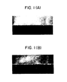
- the resulting compact and a commercially available A1 2 0 3 -TiC compact were machined into wafers, polished to give a surface roughness of 100 ⁇ , coated with A1 2 0 3 in a thickness of 10p by vapour deposition and then subjected to slicing using a diamond wheel. Consequently, it was found that the zirconia compact of the present invention had few voids as defects on the wafer surface after polishing and exhibited an excellent smoothness. As to the chipping of the edges by slicing, the zirconia compact showed 1 and A1 2 0 3 -TiC compact for comparison showed about 10, represented by a relative value of existence density of chippings of at least 10; occurring on the sliced surface.
- Figure 1 (A) and Figure 1 (B) show respectively the states of both the compacts after slicing.
- the zirconia compact wafer was provided with a magnetic head circuit by patterning, sliced and then assembled into a flying disc head which was then subjected to assessment of the characteristics as a magnetic head, while the comparative sample was similarly treated.
- the results obtained are shown under samples (1) and (10) respectively in Table 1.
- the substrates of the present invention are particularly excellent in machinability.
- Example 2 The procedure of Example 1 was repeated except using, as the hard phase, T 0.5 W 0.5 C, TiC 0.5 N 0.5 , TaC TiO 0.3 N 0.7 and TiC 0.5 N 0.2 O 0.3 instead of TiC and subjected to a similar assessment, thus obtaining the results shown in Table 2. It was found that the use of these hard phases was also effective.
- Example 2 The sintered compacts obtained in Example 2 were worked into thin film magnetic heads and practically used as a flying disc head. Consequently, it was found that the performance of these thin film magnetic heads favourably compared with that using the A1 2 O 3 -TiC substrate of the prior art.
- Example 1 The procedure of Example 1 was repeated, omitting TiC; a thin film magnetic head with a similarly good performance was obtained.
Landscapes
- Engineering & Computer Science (AREA)
- Manufacturing & Machinery (AREA)
- Magnetic Heads (AREA)
- Compositions Of Oxide Ceramics (AREA)
- Thin Magnetic Films (AREA)
Applications Claiming Priority (2)
| Application Number | Priority Date | Filing Date | Title |
|---|---|---|---|
| JP59027719A JPS60171617A (ja) | 1984-02-15 | 1984-02-15 | 薄膜磁気ヘツド用セラミツク基板 |
| JP27719/84 | 1984-02-15 |
Publications (3)
| Publication Number | Publication Date |
|---|---|
| EP0153141A2 true EP0153141A2 (de) | 1985-08-28 |
| EP0153141A3 EP0153141A3 (en) | 1988-09-14 |
| EP0153141B1 EP0153141B1 (de) | 1991-10-09 |
Family
ID=12228813
Family Applications (1)
| Application Number | Title | Priority Date | Filing Date |
|---|---|---|---|
| EP85300942A Expired EP0153141B1 (de) | 1984-02-15 | 1985-02-13 | Dünnfilmmagnetköpfe |
Country Status (5)
| Country | Link |
|---|---|
| US (1) | US4660114A (de) |
| EP (1) | EP0153141B1 (de) |
| JP (1) | JPS60171617A (de) |
| CA (1) | CA1235145A (de) |
| DE (1) | DE3584299D1 (de) |
Cited By (4)
| Publication number | Priority date | Publication date | Assignee | Title |
|---|---|---|---|---|
| WO1988000578A1 (en) * | 1986-07-10 | 1988-01-28 | Commonwealth Scientific And Industrial Research Or | Method of forming a ceramic product |
| EP0283033A3 (en) * | 1987-03-20 | 1990-03-28 | Sumitomo Electric Industries, Limited | Ceramic substrate and preparation of the same ceramic substrate and preparation of the same |
| GB2225144A (en) * | 1988-09-17 | 1990-05-23 | Tokin Corp | Magnetic head with an improved wear-resistant surface against a recording medium |
| US5165981A (en) * | 1987-03-20 | 1992-11-24 | Sumitomo Electric Industries, Ltd. | Ceramic substrate and preparation of the same |
Families Citing this family (15)
| Publication number | Priority date | Publication date | Assignee | Title |
|---|---|---|---|---|
| JPS62278164A (ja) * | 1986-05-26 | 1987-12-03 | 住友特殊金属株式会社 | 磁気ヘツド・スライダ用材料 |
| JPS63134562A (ja) * | 1986-11-21 | 1988-06-07 | 住友特殊金属株式会社 | 磁気ヘツドスライダ用材料 |
| JPH0719459B2 (ja) * | 1987-12-03 | 1995-03-06 | 日立金属株式会社 | 浮動型磁気ヘッド |
| US5010429A (en) * | 1988-11-22 | 1991-04-23 | Hitachi Metals, Ltd. | Floating magnetic head having improved static friction coefficient |
| US5060097A (en) * | 1989-01-06 | 1991-10-22 | Hitachi, Ltd. | Magnetic disc file including a slider which exhibits reduced deformation during operation |
| JP2586639B2 (ja) * | 1989-04-14 | 1997-03-05 | 松下電器産業株式会社 | 磁気ヘッド用基板材料及びそれを用いた磁気ヘッド |
| JP2977867B2 (ja) * | 1990-06-21 | 1999-11-15 | 住友特殊金属株式会社 | 磁気ヘッドスライダ用材料 |
| US5376466A (en) * | 1991-10-17 | 1994-12-27 | Mitsubishi Materials Corporation | Cermet blade member |
| US5302461A (en) * | 1992-06-05 | 1994-04-12 | Hewlett-Packard Company | Dielectric films for use in magnetoresistive transducers |
| US5636092A (en) * | 1992-07-31 | 1997-06-03 | Matsushita Electric Industrial Co., Ltd. | Magnetic head having chromium nitride protective film for use in magnetic recording and/or reproducing apparatus and method of manufacturing the same |
| US5345353A (en) * | 1992-09-21 | 1994-09-06 | International Business Machines Corporation | Step projection air bearing slider with improved stiction performance and wear resistance |
| US5626943A (en) * | 1994-06-02 | 1997-05-06 | The Carborundum Company | Ultra-smooth ceramic substrates and magnetic data storage media prepared therefrom |
| US5480695A (en) * | 1994-08-10 | 1996-01-02 | Tenhover; Michael A. | Ceramic substrates and magnetic data storage components prepared therefrom |
| US6699450B2 (en) | 1999-01-08 | 2004-03-02 | Redunndant Materials, Inc. | Carbide material by electromagnetic processing |
| EP2471972B1 (de) * | 2006-12-13 | 2014-01-29 | Idemitsu Kosan Co., Ltd. | Sputter-Target |
Family Cites Families (8)
| Publication number | Priority date | Publication date | Assignee | Title |
|---|---|---|---|---|
| JPS5614474A (en) * | 1979-07-10 | 1981-02-12 | Matsushita Electric Industrial Co Ltd | Oxygen sensor ceramic composition |
| US4316964A (en) * | 1980-07-14 | 1982-02-23 | Rockwell International Corporation | Al2 O3 /ZrO2 ceramic |
| JPS5782172A (en) * | 1980-11-12 | 1982-05-22 | Matsushita Electric Industrial Co Ltd | Substrate ceramic for thin film magnetic head |
| JPS57135772A (en) * | 1981-01-09 | 1982-08-21 | Nippon Tungsten | Material for alumina magnetic head |
| US4745509A (en) * | 1981-08-21 | 1988-05-17 | Matsushita Electric Industrial Company, Limited | Magnetic head with improved supporter for perpendicular magnetization recording |
| JPS58121179A (ja) * | 1982-01-11 | 1983-07-19 | Kyocera Corp | 磁気ヘツドスライダ |
| DE3478162D1 (en) * | 1983-09-21 | 1989-06-15 | Hitachi Metals Ltd | A magnetic head having a non-magnetic substrate |
| JPS6066403A (ja) * | 1983-09-21 | 1985-04-16 | Hitachi Metals Ltd | 薄膜磁気ヘッド用セラミックス基板 |
-
1984
- 1984-02-15 JP JP59027719A patent/JPS60171617A/ja active Pending
-
1985
- 1985-02-07 CA CA000473747A patent/CA1235145A/en not_active Expired
- 1985-02-07 US US06/699,396 patent/US4660114A/en not_active Expired - Fee Related
- 1985-02-13 DE DE8585300942T patent/DE3584299D1/de not_active Expired - Lifetime
- 1985-02-13 EP EP85300942A patent/EP0153141B1/de not_active Expired
Cited By (4)
| Publication number | Priority date | Publication date | Assignee | Title |
|---|---|---|---|---|
| WO1988000578A1 (en) * | 1986-07-10 | 1988-01-28 | Commonwealth Scientific And Industrial Research Or | Method of forming a ceramic product |
| EP0283033A3 (en) * | 1987-03-20 | 1990-03-28 | Sumitomo Electric Industries, Limited | Ceramic substrate and preparation of the same ceramic substrate and preparation of the same |
| US5165981A (en) * | 1987-03-20 | 1992-11-24 | Sumitomo Electric Industries, Ltd. | Ceramic substrate and preparation of the same |
| GB2225144A (en) * | 1988-09-17 | 1990-05-23 | Tokin Corp | Magnetic head with an improved wear-resistant surface against a recording medium |
Also Published As
| Publication number | Publication date |
|---|---|
| US4660114A (en) | 1987-04-21 |
| EP0153141A3 (en) | 1988-09-14 |
| JPS60171617A (ja) | 1985-09-05 |
| CA1235145A (en) | 1988-04-12 |
| DE3584299D1 (en) | 1991-11-14 |
| EP0153141B1 (de) | 1991-10-09 |
Similar Documents
| Publication | Publication Date | Title |
|---|---|---|
| EP0153141A2 (de) | Dünnfilmmagnetköpfe | |
| US4681813A (en) | Ceramic substrate for a thin layer magnetic head | |
| US4608293A (en) | Composite substrate for a thin-film magnetic head | |
| US4796127A (en) | Recording head slider | |
| JPH062615B2 (ja) | 磁気ヘツドスライダ材料 | |
| US5413850A (en) | Non-conductive aluminum oxide-titanium carbide (A1203-TIC) thin film computer head substrate, method of making same, and slider element incorporating same | |
| EP0137134B1 (de) | Magnetkopf mit unmagnetischem Substrat | |
| EP0142781A2 (de) | Montage eines Magnetkopfgleiters | |
| US5432016A (en) | Magnetic head slider material | |
| KR900006677B1 (ko) | 세라믹기판 및 그 제조방법 | |
| JPH0120523B2 (de) | ||
| EP0157487B1 (de) | Keramische Presskörper, die Zirkonerde enthalten | |
| JPH0121112B2 (de) | ||
| JPH05246763A (ja) | セラミックス焼結体 | |
| JPH02180754A (ja) | 磁気ヘッドのスライダ | |
| JPH05254938A (ja) | セラミックス焼結体 | |
| JPH05217117A (ja) | 薄膜磁気ヘッド | |
| JPH05109023A (ja) | 磁気ヘツド用基板 | |
| JPS6110052A (ja) | 薄膜磁気ヘツド用基板材料 | |
| JP2581935B2 (ja) | セラミック焼結体 | |
| CA2188150A1 (en) | Improved disk substrate | |
| JPS63134559A (ja) | 磁気ヘツド用非磁性セラミツクス | |
| JPH05217118A (ja) | 薄膜磁気ヘッド | |
| JPH0373043B2 (de) | ||
| JP2616800B2 (ja) | セラミック焼結体の製法 |
Legal Events
| Date | Code | Title | Description |
|---|---|---|---|
| PUAI | Public reference made under article 153(3) epc to a published international application that has entered the european phase |
Free format text: ORIGINAL CODE: 0009012 |
|
| AK | Designated contracting states |
Designated state(s): DE FR GB NL SE |
|
| 17P | Request for examination filed |
Effective date: 19851122 |
|
| PUAL | Search report despatched |
Free format text: ORIGINAL CODE: 0009013 |
|
| AK | Designated contracting states |
Kind code of ref document: A3 Designated state(s): DE FR GB NL SE |
|
| 17Q | First examination report despatched |
Effective date: 19900322 |
|
| GRAA | (expected) grant |
Free format text: ORIGINAL CODE: 0009210 |
|
| AK | Designated contracting states |
Kind code of ref document: B1 Designated state(s): DE FR GB NL SE |
|
| REF | Corresponds to: |
Ref document number: 3584299 Country of ref document: DE Date of ref document: 19911114 |
|
| ET | Fr: translation filed | ||
| PLBE | No opposition filed within time limit |
Free format text: ORIGINAL CODE: 0009261 |
|
| STAA | Information on the status of an ep patent application or granted ep patent |
Free format text: STATUS: NO OPPOSITION FILED WITHIN TIME LIMIT |
|
| 26N | No opposition filed | ||
| EAL | Se: european patent in force in sweden |
Ref document number: 85300942.1 |
|
| PGFP | Annual fee paid to national office [announced via postgrant information from national office to epo] |
Ref country code: FR Payment date: 19960125 Year of fee payment: 12 |
|
| PGFP | Annual fee paid to national office [announced via postgrant information from national office to epo] |
Ref country code: GB Payment date: 19960205 Year of fee payment: 12 |
|
| PGFP | Annual fee paid to national office [announced via postgrant information from national office to epo] |
Ref country code: SE Payment date: 19960215 Year of fee payment: 12 Ref country code: DE Payment date: 19960215 Year of fee payment: 12 |
|
| PGFP | Annual fee paid to national office [announced via postgrant information from national office to epo] |
Ref country code: NL Payment date: 19960229 Year of fee payment: 12 |
|
| PG25 | Lapsed in a contracting state [announced via postgrant information from national office to epo] |
Ref country code: GB Effective date: 19970213 |
|
| PG25 | Lapsed in a contracting state [announced via postgrant information from national office to epo] |
Ref country code: SE Effective date: 19970214 |
|
| PG25 | Lapsed in a contracting state [announced via postgrant information from national office to epo] |
Ref country code: NL Effective date: 19970901 |
|
| GBPC | Gb: european patent ceased through non-payment of renewal fee |
Effective date: 19970213 |
|
| PG25 | Lapsed in a contracting state [announced via postgrant information from national office to epo] |
Ref country code: FR Effective date: 19971030 |
|
| PG25 | Lapsed in a contracting state [announced via postgrant information from national office to epo] |
Ref country code: DE Effective date: 19971101 |
|
| EUG | Se: european patent has lapsed |
Ref document number: 85300942.1 |
|
| NLV4 | Nl: lapsed or anulled due to non-payment of the annual fee |
Effective date: 19970901 |
|
| REG | Reference to a national code |
Ref country code: FR Ref legal event code: ST |