EP0155215A2 - Halbleiteranordnung hoher Elektronenbeweglichkeit mit selektiv dotiertem Heteroübergang - Google Patents
Halbleiteranordnung hoher Elektronenbeweglichkeit mit selektiv dotiertem Heteroübergang Download PDFInfo
- Publication number
- EP0155215A2 EP0155215A2 EP85400448A EP85400448A EP0155215A2 EP 0155215 A2 EP0155215 A2 EP 0155215A2 EP 85400448 A EP85400448 A EP 85400448A EP 85400448 A EP85400448 A EP 85400448A EP 0155215 A2 EP0155215 A2 EP 0155215A2
- Authority
- EP
- European Patent Office
- Prior art keywords
- layer
- spacer
- gaas
- electron mobility
- high electron
- Prior art date
- Legal status (The legal status is an assumption and is not a legal conclusion. Google has not performed a legal analysis and makes no representation as to the accuracy of the status listed.)
- Granted
Links
Images




Classifications
-
- H—ELECTRICITY
- H10—SEMICONDUCTOR DEVICES; ELECTRIC SOLID-STATE DEVICES NOT OTHERWISE PROVIDED FOR
- H10D—INORGANIC ELECTRIC SEMICONDUCTOR DEVICES
- H10D30/00—Field-effect transistors [FET]
- H10D30/40—FETs having zero-dimensional [0D], one-dimensional [1D] or two-dimensional [2D] charge carrier gas channels
- H10D30/47—FETs having zero-dimensional [0D], one-dimensional [1D] or two-dimensional [2D] charge carrier gas channels having two-dimensional [2D] charge carrier gas channels, e.g. nanoribbon FETs or high electron mobility transistors [HEMT]
- H10D30/471—High electron mobility transistors [HEMT] or high hole mobility transistors [HHMT]
- H10D30/475—High electron mobility transistors [HEMT] or high hole mobility transistors [HHMT] having wider bandgap layer formed on top of lower bandgap active layer, e.g. undoped barrier HEMTs such as i-AlGaN/GaN HEMTs
- H10D30/4755—High electron mobility transistors [HEMT] or high hole mobility transistors [HHMT] having wider bandgap layer formed on top of lower bandgap active layer, e.g. undoped barrier HEMTs such as i-AlGaN/GaN HEMTs having wide bandgap charge-carrier supplying layers, e.g. modulation doped HEMTs such as n-AlGaAs/GaAs HEMTs
-
- H—ELECTRICITY
- H10—SEMICONDUCTOR DEVICES; ELECTRIC SOLID-STATE DEVICES NOT OTHERWISE PROVIDED FOR
- H10D—INORGANIC ELECTRIC SEMICONDUCTOR DEVICES
- H10D30/00—Field-effect transistors [FET]
- H10D30/40—FETs having zero-dimensional [0D], one-dimensional [1D] or two-dimensional [2D] charge carrier gas channels
- H10D30/47—FETs having zero-dimensional [0D], one-dimensional [1D] or two-dimensional [2D] charge carrier gas channels having two-dimensional [2D] charge carrier gas channels, e.g. nanoribbon FETs or high electron mobility transistors [HEMT]
- H10D30/471—High electron mobility transistors [HEMT] or high hole mobility transistors [HHMT]
- H10D30/473—High electron mobility transistors [HEMT] or high hole mobility transistors [HHMT] having confinement of carriers by multiple heterojunctions, e.g. quantum well HEMT
- H10D30/4732—High electron mobility transistors [HEMT] or high hole mobility transistors [HHMT] having confinement of carriers by multiple heterojunctions, e.g. quantum well HEMT using Group III-V semiconductor material
Definitions
- This invention relates to a semiconductor device with enhanced mobility employing selectively doped heterojunction, and especially, to a structure of a semiconductor device which enables a high temperature treatment without disturbing the electron mobility of the two-dimensional electron gas, in order to install the device in an integrated circuit (IC).
- IC integrated circuit
- Gallium arsenide is one of such new materials which has a capability to obtain a higher operating speed because of its electron mobility higher than that of silicon, and devices using such a material are now under development.
- the field effect transistor As a device utilizing compound semiconductor material such as gallium arsenide, the field effect transistor (FET) is ahead of development because its fabrication process is simple compared to that of a bipolar transistor.
- the Schottky barrier type FET whose parasitic capacitance is reduced by using a semi-insulating substrate of compound semiconductor is becoming a main stream of the development.
- carriers move through semiconductor lattice space where impurity ions are existing.
- the carrier have their motion affected by the lattice and the impurity ions, and loose their mobility by collision and scattering therewith. It is possible to decrease the effect of scattering by lattice (interaction with phonon) by decreasing the temperature, but it increases the scattering by impurity ions so that the mobility of the carriers is limited.
- Fig. 1 (a) and Fig. l(b) show two types of prior art heterojunction FETs including a semi-insulating gallium arsenide (GaAs) substrate 1 which, in some cases, is intentionally doped with chromium(Cr) or iron (Fe) etc. to compensate the effect of unintentionally doped impurities, and provide a very high resistivity.
- GaAs gallium arsenide
- Fe iron
- an undoped i-type GaAs layer 2 On the substrate 1 are piled, in order from the surface of the substrate, an undoped i-type GaAs layer 2, an aluminum-gallium arsenide (Al x Ga 1 -x As) layer 3 having an electron affinity smaller than that of the layer 2, and an n-type GaAs layer 4.
- the n-type GaAs layer 4 is highly doped to secure a good contact with contact wires and shaped is to form source and drain electrodes as shown in Figs. l(a) and l(b).
- the Al Ga.._ As layer 3 is doped with silicon (Si), for example, and is of the n-type.
- Carriers (in this case electron) formed in the doped layer 3 are transferred to the undoped layer 2 and accumulates in the layer 2 near the heterojunction between the i-type GaAs layer 2 and the Al x Ga 1-x As layer 3, and form a two-dimensional electron gas 2A as shown in the figure.
- This two-dimensional electron gas (abbreviated as 2DEG) plays the role of a channel in the FET, and is often designated as channel layer.
- the lattice scattering decreases, and since the i-type GaAs layer 2 is not doped and has very rare ionized impurities, the 2DEG is not affected by the scattering by the ions and sustains a high mobility. Thus, a high speed operation of the heterojunction FET is attained.
- Fig. l(a) it has been found that in the structure of Fig. l(a) some of the carriers in the 2DEG 2A are affected by the ions in the Al x Ga-1-x As layer 3, so that the mobility of the carriers may not be sufficiently high. It has then been proposed to provide a buffer zone or spacer between the 2DEG and the carrier supplying layer (reference can be made for example to U.S. Pat. 4,163,237).
- Fig. l(b) shows an example of such a structure. Compared to Fig. l(a), the Al x Ga 1-x layer 3 is subdivided into two layers 3a and 3b.
- a thin layer 3a of undoped Al x Ga 1-x As which acts as buffer zone or spacer.
- the carrier supplying layer 3b which is a Si doped layer for example.
- the thickness of the buffer zone is a few tens of (between 1 0 -9 and 10 -8 m ) .
- the 2DEG shows a mobility of 1 x 1 0 5 cm 2 /V.s at 77°K, with a 2DEG concentration of 6 x 10 11 cm -2 and the high speed operation of GaAs FETs has been improved to a great extent.
- the GaAs FETs having the above mentioned structure have been fabricated with a processing temperature fairly low compared to that of ordinary semiconductor or manufacturing process.
- the source or drain electrode has been fabricated with an eutectic alloy of gold and gold-germanium (AuGe/Au) whose eutectic temperature is 450°C, and the heating time has been kept to less than one minute.
- the thermal diffusion of impurities from the doped Al x Ga 1-x As layer 3b into the spacer region of undoped Al x Ga 1-x As layer 3a has been suppressed. If not, the impurity in the layer 3b will diffuse into the spacer layer 3a, and cause the mobility to decrease by interaction with the impurity ions.
- Another object of the present invention is to provide a high electron mobility transistor (HEMT) which can be used together with other electron devices as an integrated circuit.
- HEMT high electron mobility transistor
- the spacer layer of Al x Ga 1-x As has an effect to prevent the interaction between the ionized impurities in the doped layer of Al x Ga 1-x As (3b in Fig. l(b), but has no ability to prevent the diffusion of impurity ions from the layer 3b into the layer 3a (spacer).
- the Si impurity is distributed uniformly in both Al x Ga 1-x As layers 3a and 3b.
- the layer of undoped GaAs layer i-GaAs has shown an effect to stop the diffusion of Si.
- the inventors have provided a second spacer consisting in an undoped GaAs (i-GaAs) layer over the prior art spacer formed of an undoped Al x Ga 1-x As (i-Al x Ga 1-x As) layer, the carrier supplying layer of Si doped n-Al x Ga 1-x As being fabricated over the second spacer.
- i-GaAs undoped GaAs
- i-Al x Ga 1-x As undoped Al x Ga 1-x As
- the carrier supplying layer of Si doped n-Al x Ga 1-x As being fabricated over the second spacer.
- the thickness of the second spacer is preferably comprised between 15 and 30A (1.5x10 -9 and 3x 10 m), for example approximately 20A (2 x 10 -9 m), whereas the first spacer (i-Al x Ga 1-x As layer) has a thickness preferably comprised between 20 and 40 A (2x10 -9 and 4x10 -9 m), for example approximately 40 ⁇ (4x10 -9 m) .
- the undoped Al x Ga 1-x As layer has no effect to prevent the diffusion of Si.
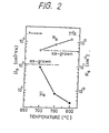
- the heating time has been reduced.
- a substrate having the same structure as in the above case has been annealed by means of a tungsten-halogen lamp heater for 10 seconds, and ⁇ s and N s have been measured at 77°K. Reducing the heating time is an effective method often used to avoid the defects of heating. However, as shown in Fig. 3, the mobility decreases even with a short time treatment of 10 seconds.
- a layer of Al O.3 Ga O.7 As has been grown on a high resistivity GaAs substrated by molecular beam epitaxy.
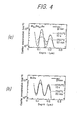
- the doping rate at various depth has been intentionally varied (such doping is sometimes called modulated doping) as shown in Fig. 4 (a).
- the abscissa is the distance from the surface of the grown layer toward the substrate, and the ordinate is the carrier concentration measured by capacitance-voltage (C-V) method.
- the heavy line indicates the concentration of the layer as grown.
- the substrate has been thermally processed by means of tungsten-halogen lamps (1050°C, 10 s) and by means of a conventional furnace (750°C 20 min).
- the dotted curve and the broken line respectively show the concentration after the above treatments.
- the curves show that Si is easily redistributed in the Al 0.3 Ga 0.7 As layer by thermal diffusion. This indicates that the spacer layer is easily penetrated by Si impurity when it is thermally treated.
- GaAs layer has been grown on a high resistivity GaAs substrate by molecular beam epitaxy, and the doping has been varied as in the above case, i.e. as shown by the heavy line of Fig. 4(a). Measurement of carrier concentration has been made under the same conditions as precedingly. As can be seen from Fig. 4(b) the GaAs layer shows far less redistribution of Si in it compared to Al x G a 1-x As. This indicates the possibility of forming a spacer with an undoped GaAs layer (i-GaAs layer).
- the substrate thus prepared has been cut into two parts; the impurity distribution of the Al Ga-1-xAs layer as grown has been measured on one part (curve 2); the other part has been thermally treated at 750°C for 80 minutes in a furnace, then the impurity distribution has been measured (curve B). In both cases, the impurity (Si) concentration has been measured by secondary ion mass spectroscopy (SIMS).
- Si secondary ion mass spectroscopy
- a practical multilayered structure according to the present invention has been determined from a computer aided simulation of energy band diagram and carrier concentration as shown in Fig. 6 by way of example.
- HEMT neighbor electron mobility transistor
- n + regions 17 having a carrier concentration of approximately 4-5 x 10 18 cm -3 are formed.
- the source electrode 18 and drain electrode 19 are fabricated.
- a recess is made in the n-GaAs layer to expose the layer 15 for contacting a gate electrode 20 thereto.
- Fig. 6 shows the energy band diagram and space distribution of the 2DEG near the channel region.
- the abscissa is the distance from the surface of the n-Al x Ga 1-x As layer 15, and the ordinate is the energy level.
- the curve C shows the energy level at each level of the cross-section of Fig. 7 and the curve 12A shows the concentration of the 2DEG with an arbitrary scale. These curves are obtained by computer simulation. When the width of the spacers 14 and 13 are varied, the 2DEG concentration varies.
- the curves of Fig. 6 correspond to the embodiment described with respect to Fig. 7, namely the widths of the first spacer 13 and of the second spacer 14 are being equal to 40 A (4x10 -9 m) and 20 ⁇ (2x10 -9 m), respectively, which is considered to be favourable.
- the total width of the two spacers should be less than 100 A (10x10 -9 m) and preferably below approximately 60 A (6x10 -9 m) or less. If the total width is increased, the 2DEG concentration decreases, so that the g m of the FET will decrease. On the contrary when the width of the spacers is too much decreased, the concentration of the 2DEG in the spacer layer 13 will increase causing the scattering by the impurity ions in the layer 15 also to increase, and the mobility decreases. For this reason, it is desirable that the spacer layer 13 has a thickness larger than approximately 20 A (2x10 -9 m). The thickness of the second spacer layer 14 should be as small as possible. But, if it is too much decreased, the diffusion of impurity occurs. A thickness of approximately 15 A (1.5x10 -9 m) is preferred. The dimensions of the structure of Fig. 7 has been thus determined.
- the potential well D in Fig. 6 formed by the second spacer layer 14 has a capacity to capture and accumulate carriers in it, but since its width is very thin, the number of carriers (E in Fig. 6) captured by the potential well D is not so high. However, if the width of the second spacer layer 14 is increased, the charge captured in the potential well increases and causes an increase of impurity ion scattering, and the mobility is decreased. Therefore, the thickness of the second spacer 14 layer is preferably less than approximately 30 A (3x10 -9 m).
- a substrate having the structure of Fig. 7 has been thermally treated during its fabrication process including a treatment at 750°C for 10 minutes and lamp annealing at 950°C. It has been further thermally treated for test with a tungsten-halogen lamp for 10 seconds at various temperatures, and the mobility and carrier concentration has been measured.
- Fig. 8 shows the results obtained. Compared to the curves of Fig. 3, the mobility does not decrease at 900°C, and keeps approximately its high value up to nearly 1,000°C.
- the structure of the present invention improves the durability of the multilayered heterojunction device at high temperatures, compared to the structures of the prior art, and keeps its high electron mobility. Therefore, the structure of the present invention is applicable to the making of ICs comprising high electron mobility transistors (HEMT).
- HEMT high electron mobility transistors
- the above disclosure has been made with respect to an n-channel FET, because the election mobility is higher than that of the holes,this giving an advantage to n-channel devices over p-channel devices for high speed devices. But it will be clear for anyone skilled in the art that the invention can be easily extended to p-channel devices.
- the invention is also not limited to the materials and processes used in the above described embodiment and any kind of other material or technology which is suitable for fabricating the structure of the device according to the invention may be used.
- the heterojunction which accumulates the 2DEG (channel layer) is not limited to be formed by only one layer; a multilayered channel with an interleaving of a plurality of heterojunction layers can be used within the spirit and scope of the present invention.
Landscapes
- Junction Field-Effect Transistors (AREA)
Applications Claiming Priority (2)
| Application Number | Priority Date | Filing Date | Title |
|---|---|---|---|
| JP44501/84 | 1984-03-08 | ||
| JP59044501A JPS60189268A (ja) | 1984-03-08 | 1984-03-08 | 半導体装置 |
Publications (3)
| Publication Number | Publication Date |
|---|---|
| EP0155215A2 true EP0155215A2 (de) | 1985-09-18 |
| EP0155215A3 EP0155215A3 (en) | 1986-02-19 |
| EP0155215B1 EP0155215B1 (de) | 1988-07-20 |
Family
ID=12693295
Family Applications (1)
| Application Number | Title | Priority Date | Filing Date |
|---|---|---|---|
| EP85400448A Expired EP0155215B1 (de) | 1984-03-08 | 1985-03-08 | Halbleiteranordnung hoher Elektronenbeweglichkeit mit selektiv dotiertem Heteroübergang |
Country Status (6)
| Country | Link |
|---|---|
| US (1) | US4593301A (de) |
| EP (1) | EP0155215B1 (de) |
| JP (1) | JPS60189268A (de) |
| KR (1) | KR890004452B1 (de) |
| CA (1) | CA1220876A (de) |
| DE (1) | DE3563897D1 (de) |
Cited By (4)
| Publication number | Priority date | Publication date | Assignee | Title |
|---|---|---|---|---|
| DE3706274A1 (de) * | 1986-02-28 | 1987-09-03 | Hitachi Ltd | Halbleiterelement und verfahren zu dessen herstellung |
| FR2600821A1 (fr) * | 1986-06-30 | 1987-12-31 | Thomson Csf | Dispositif semi-conducteur a heterojonction et double canal, son application a un transistor a effet de champ, et son application a un dispositif de transductance negative |
| US4855797A (en) * | 1987-07-06 | 1989-08-08 | Siemens Corporate Research And Support, Inc. | Modulation doped high electron mobility transistor with n-i-p-i structure |
| GB2248967A (en) * | 1990-10-19 | 1992-04-22 | Philips Electronic Associated | A high mobility semiconductor device |
Families Citing this family (25)
| Publication number | Priority date | Publication date | Assignee | Title |
|---|---|---|---|---|
| DE3334167A1 (de) * | 1983-09-21 | 1985-04-04 | Siemens AG, 1000 Berlin und 8000 München | Halbleiterdiode |
| KR900001394B1 (en) * | 1985-04-05 | 1990-03-09 | Fujitsu Ltd | Super high frequency intergrated circuit device |
| JPH088350B2 (ja) * | 1985-04-08 | 1996-01-29 | 日本電気株式会社 | 半導体装置 |
| US4710478A (en) * | 1985-05-20 | 1987-12-01 | United States Of America As Represented By The Secretary Of The Navy | Method for making germanium/gallium arsenide high mobility complementary logic transistors |
| USH411H (en) | 1985-08-28 | 1988-01-05 | United States Of America | Quasi-accumulation mode FET |
| US4745448A (en) * | 1985-12-24 | 1988-05-17 | Raytheon Company | Semiconductor devices having compensated buffer layers |
| US5181087A (en) * | 1986-02-28 | 1993-01-19 | Hitachi, Ltd. | Semiconductor device and method of producing the same |
| KR880010509A (ko) * | 1987-02-11 | 1988-10-10 | 오레그 이. 앨버 | 전계효과 트랜지스터 |
| DE3881922T2 (de) * | 1987-03-18 | 1993-10-07 | Fujitsu Ltd | Zusammengesetzte Halbleiteranordnung mit nicht-legierten ohmschen Kontakten. |
| US4965645A (en) * | 1987-03-20 | 1990-10-23 | International Business Machines Corp. | Saturable charge FET |
| JP2536523B2 (ja) * | 1987-05-14 | 1996-09-18 | 日本電気株式会社 | 半導体装置の製造方法 |
| JPS63314850A (ja) * | 1987-06-18 | 1988-12-22 | Fujitsu Ltd | 半導体装置 |
| JPH01132170A (ja) * | 1987-11-18 | 1989-05-24 | Toshiba Corp | 電界効果トランジスタ |
| US4962050A (en) * | 1988-12-06 | 1990-10-09 | Itt Corporation | GaAs FET manufacturing process employing channel confining layers |
| DE3842863A1 (de) * | 1988-12-20 | 1990-06-21 | Fraunhofer Ges Forschung | Feldeffekttransistor und verfahren zum herstellen eines feldeffekttransistors |
| DE69031813T2 (de) * | 1989-04-04 | 1998-04-09 | Siemens Ag | HEMT-Struktur |
| JPH03145139A (ja) * | 1989-10-30 | 1991-06-20 | Mitsubishi Electric Corp | 電界効果トランジスタとその製造方法 |
| US5242846A (en) * | 1989-10-30 | 1993-09-07 | Mitsubishi Denki Kabushiki Kaisha | Method of manufacturing a junction field effect transistor |
| KR910013568A (ko) * | 1989-12-31 | 1991-08-08 | 김광호 | 화합물 반도체 장치 및 그 제조방법 |
| DE4123939A1 (de) * | 1991-07-19 | 1993-01-21 | Daimler Benz Ag | Heterostruktur-feldeffekttransistor mit pulsdotiertem kanal |
| JP2687897B2 (ja) * | 1994-10-13 | 1997-12-08 | 日本電気株式会社 | 電界効果型トランジスタ及びその製造方法 |
| JP3601649B2 (ja) * | 1996-12-25 | 2004-12-15 | 株式会社村田製作所 | 電界効果トランジスタ |
| WO2003015174A2 (en) * | 2001-08-07 | 2003-02-20 | Jan Kuzmik | High electron mobility devices |
| JP4050128B2 (ja) * | 2002-10-24 | 2008-02-20 | 松下電器産業株式会社 | ヘテロ接合電界効果型トランジスタ及びその製造方法 |
| JP4940557B2 (ja) * | 2005-02-08 | 2012-05-30 | 日本電気株式会社 | 電界効果トランジスタ及びその製造方法 |
Family Cites Families (2)
| Publication number | Priority date | Publication date | Assignee | Title |
|---|---|---|---|---|
| US4163237A (en) * | 1978-04-24 | 1979-07-31 | Bell Telephone Laboratories, Incorporated | High mobility multilayered heterojunction devices employing modulated doping |
| JPS5728322A (en) * | 1980-07-28 | 1982-02-16 | Fujitsu Ltd | Formation of semiconductor single crystal layer |
-
1984
- 1984-03-08 JP JP59044501A patent/JPS60189268A/ja not_active Expired - Lifetime
-
1985
- 1985-03-01 US US06/707,290 patent/US4593301A/en not_active Expired - Lifetime
- 1985-03-06 KR KR1019850001433A patent/KR890004452B1/ko not_active Expired
- 1985-03-07 CA CA000475887A patent/CA1220876A/en not_active Expired
- 1985-03-08 EP EP85400448A patent/EP0155215B1/de not_active Expired
- 1985-03-08 DE DE8585400448T patent/DE3563897D1/de not_active Expired
Cited By (6)
| Publication number | Priority date | Publication date | Assignee | Title |
|---|---|---|---|---|
| DE3706274A1 (de) * | 1986-02-28 | 1987-09-03 | Hitachi Ltd | Halbleiterelement und verfahren zu dessen herstellung |
| FR2600821A1 (fr) * | 1986-06-30 | 1987-12-31 | Thomson Csf | Dispositif semi-conducteur a heterojonction et double canal, son application a un transistor a effet de champ, et son application a un dispositif de transductance negative |
| EP0255416A1 (de) * | 1986-06-30 | 1988-02-03 | Thomson-Csf | Halbleiteranordnung mit Heteroübergängen und zwei Kanälen, ihre Verwendung beim Feldeffekttransistor und ihre Verwendung bei einer Anordnung mit negativer Transduktanz |
| US4806998A (en) * | 1986-06-30 | 1989-02-21 | Thomson-Csf | Heterojunction and dual channel semiconductor field effect transistor or negative transconductive device |
| US4855797A (en) * | 1987-07-06 | 1989-08-08 | Siemens Corporate Research And Support, Inc. | Modulation doped high electron mobility transistor with n-i-p-i structure |
| GB2248967A (en) * | 1990-10-19 | 1992-04-22 | Philips Electronic Associated | A high mobility semiconductor device |
Also Published As
| Publication number | Publication date |
|---|---|
| DE3563897D1 (en) | 1988-08-25 |
| EP0155215A3 (en) | 1986-02-19 |
| JPS60189268A (ja) | 1985-09-26 |
| EP0155215B1 (de) | 1988-07-20 |
| US4593301A (en) | 1986-06-03 |
| KR850006788A (ko) | 1985-10-16 |
| KR890004452B1 (ko) | 1989-11-04 |
| CA1220876A (en) | 1987-04-21 |
Similar Documents
| Publication | Publication Date | Title |
|---|---|---|
| EP0155215B1 (de) | Halbleiteranordnung hoher Elektronenbeweglichkeit mit selektiv dotiertem Heteroübergang | |
| CA1142274A (en) | Vertical field effect transistor | |
| CA1125924A (en) | Nonalloyed ohmic contacts to n-type group iii(a)-v(a) semiconductors | |
| EP0397987A1 (de) | Silicium-MOSFET mit Germanium-Kanal | |
| US5677553A (en) | Semiconductor device strucutre having a two-dimensional electron gas and contact thereto | |
| US4662058A (en) | Self-aligned gate process for ICS based on modulation doped (Al,Ga) As/GaAs FETs | |
| EP0064829A2 (de) | Halbleiteranordnung mit hoher Elektronenbeweglichkeit und Verfahren zu deren Herstellung | |
| US4673959A (en) | Heterojunction FET with doubly-doped channel | |
| KR920003799B1 (ko) | 반도체 장치 | |
| JPS5925392B2 (ja) | 電界効果トランジスタ及びその製造方法 | |
| EP0080714B1 (de) | Halbleiteranordnung mit Heteroübergängen | |
| JPS61256675A (ja) | シヨツトキゲ−ト電界効果トランジスタの製造方法 | |
| US5276340A (en) | Semiconductor integrated circuit having a reduced side gate effect | |
| EP0115668B1 (de) | Halbleitervorrichtung mit Heteroübergang | |
| US4764796A (en) | Heterojunction field effect transistor with two-dimensional electron layer | |
| JPS61248470A (ja) | ▲iii▼―▲v▼族半導体デバイス | |
| US5107314A (en) | Gallium antimonide field-effect transistor | |
| JPS593977A (ja) | 半導体装置 | |
| JPS6354231B2 (de) | ||
| JPS59100577A (ja) | 半導体装置 | |
| KR910006698B1 (ko) | 반도체 장치 | |
| JPH02201934A (ja) | チャンネル限定層を使用するGaAs FETの製造方法 | |
| EP0437702B1 (de) | Integrierte Halbleiterschaltung mit Isolationszonen zwischen Komponenten aus Verbindungshalbleitern und Methode zu deren Herstellung | |
| US5693969A (en) | MESFET having a termination layer in the channel layer | |
| JPH0810701B2 (ja) | 接合型電界効果トランジスタの製造方法 |
Legal Events
| Date | Code | Title | Description |
|---|---|---|---|
| PUAI | Public reference made under article 153(3) epc to a published international application that has entered the european phase |
Free format text: ORIGINAL CODE: 0009012 |
|
| AK | Designated contracting states |
Designated state(s): DE FR GB IT |
|
| PUAL | Search report despatched |
Free format text: ORIGINAL CODE: 0009013 |
|
| AK | Designated contracting states |
Designated state(s): DE FR GB IT |
|
| 17P | Request for examination filed |
Effective date: 19860314 |
|
| 17Q | First examination report despatched |
Effective date: 19870902 |
|
| GRAA | (expected) grant |
Free format text: ORIGINAL CODE: 0009210 |
|
| AK | Designated contracting states |
Kind code of ref document: B1 Designated state(s): DE FR GB IT |
|
| REF | Corresponds to: |
Ref document number: 3563897 Country of ref document: DE Date of ref document: 19880825 |
|
| ITF | It: translation for a ep patent filed | ||
| ET | Fr: translation filed | ||
| PLBE | No opposition filed within time limit |
Free format text: ORIGINAL CODE: 0009261 |
|
| STAA | Information on the status of an ep patent application or granted ep patent |
Free format text: STATUS: NO OPPOSITION FILED WITHIN TIME LIMIT |
|
| 26N | No opposition filed | ||
| ITTA | It: last paid annual fee | ||
| REG | Reference to a national code |
Ref country code: GB Ref legal event code: IF02 |
|
| PGFP | Annual fee paid to national office [announced via postgrant information from national office to epo] |
Ref country code: GB Payment date: 20040303 Year of fee payment: 20 |
|
| PGFP | Annual fee paid to national office [announced via postgrant information from national office to epo] |
Ref country code: FR Payment date: 20040309 Year of fee payment: 20 |
|
| PGFP | Annual fee paid to national office [announced via postgrant information from national office to epo] |
Ref country code: DE Payment date: 20040318 Year of fee payment: 20 |
|
| PG25 | Lapsed in a contracting state [announced via postgrant information from national office to epo] |
Ref country code: GB Free format text: LAPSE BECAUSE OF EXPIRATION OF PROTECTION Effective date: 20050307 |
|
| REG | Reference to a national code |
Ref country code: GB Ref legal event code: PE20 |