EP0159042A2 - Gerät zum Herabsetzen von Geräuschen in Audiosignalen - Google Patents
Gerät zum Herabsetzen von Geräuschen in Audiosignalen Download PDFInfo
- Publication number
- EP0159042A2 EP0159042A2 EP85104736A EP85104736A EP0159042A2 EP 0159042 A2 EP0159042 A2 EP 0159042A2 EP 85104736 A EP85104736 A EP 85104736A EP 85104736 A EP85104736 A EP 85104736A EP 0159042 A2 EP0159042 A2 EP 0159042A2
- Authority
- EP
- European Patent Office
- Prior art keywords
- signal
- noise
- reproduced
- detector
- dropout
- Prior art date
- Legal status (The legal status is an assumption and is not a legal conclusion. Google has not performed a legal analysis and makes no representation as to the accuracy of the status listed.)
- Granted
Links
Images


Classifications
-
- G—PHYSICS
- G11—INFORMATION STORAGE
- G11B—INFORMATION STORAGE BASED ON RELATIVE MOVEMENT BETWEEN RECORD CARRIER AND TRANSDUCER
- G11B20/00—Signal processing not specific to the method of recording or reproducing; Circuits therefor
- G11B20/24—Signal processing not specific to the method of recording or reproducing; Circuits therefor for reducing noise
-
- G—PHYSICS
- G11—INFORMATION STORAGE
- G11B—INFORMATION STORAGE BASED ON RELATIVE MOVEMENT BETWEEN RECORD CARRIER AND TRANSDUCER
- G11B20/00—Signal processing not specific to the method of recording or reproducing; Circuits therefor
- G11B20/02—Analogue recording or reproducing
- G11B20/025—Error detection or correction
-
- H—ELECTRICITY
- H03—ELECTRONIC CIRCUITRY
- H03G—CONTROL OF AMPLIFICATION
- H03G3/00—Gain control in amplifiers or frequency changers
- H03G3/20—Automatic control
- H03G3/30—Automatic control in amplifiers having semiconductor devices
- H03G3/34—Muting amplifier when no signal is present
- H03G3/345—Muting during a short period of time when noise pulses are detected, i.e. blanking
-
- H—ELECTRICITY
- H03—ELECTRONIC CIRCUITRY
- H03G—CONTROL OF AMPLIFICATION
- H03G3/00—Gain control in amplifiers or frequency changers
- H03G3/20—Automatic control
- H03G3/30—Automatic control in amplifiers having semiconductor devices
- H03G3/34—Muting amplifier when no signal is present
- H03G3/348—Muting in response to a mechanical action or to power supply variations, e.g. during tuning; Click removal circuits
Definitions
- the present invention relates to an apparatus for reducing noise in audio signals for use in a rotary head magnetic recording and reproducing system of a helical-scan type in which a magnetic tape, which is wrapped helically on the surface of a rotary cylinder at a given angle with the axis of rotation of the rotary cylinder, is fed along a path of rotation for at least one magnetic head provided on the rotary cylinder so that the magnetic head successively records and reproduces audio signals in and from a group of record patterns in the magnetic tape inclined relative to the longitudinal direction of the magnetic tape.
- an audio signal modulated wave reproduced by a magnetic head which is provided on a rotary cylinder, is demodulated to pass through a phase shifter for shifting the phase of the demodulated audio signal, thereby generating two signals which are different in the phase.
- a hold circuit which operates in synchronism with the successive switching between the record patterns in a magnetic tape to be reproduced and also operates in response to the occurrence of dropout noise in the reproduced signal of the modulated wave, and a sum output signal of output signals from the two hold circuits is obtained thereby to attain the reduction of noise.
- Numeral 1 designates an input terminal to which a reproduced signal of the modulated wave is applied
- 2 a detector for detecting the magnitude of the reproduced modulated wave signal applied to the input terminal 1
- 3 a demodulator, 4 and 6 amplifiers, 5 and 10 switches which are switched off in response to the operation of the detector 2, 7 and 11 holding capacitors, 8 an output terminal, and 9 an all-pass circuit which is connected to an output of the amplifier 4 to operate as a phase shifter and includes an operational amplifier 9a, resistors 9b and 9c connected respectively to inverting and non-inverting input terminals to the operational amplifier 9a, a resistor 9d connected across an output terminal and the inverting input terminal of the operational amplifier 9a and a capacitor 9e connected across the non-inverting input terminal and the ground.
- the switch 10 is responsive to the operation of the detector 2 and applies an output signal F of the all-pass circuit 9 to an input terminal to the amplifier 6.
- the capacitor 11 has an end thereof connected to the input terminal of the amplifier 6 and the other end thereof connected to the ground.
- Numeral 12 designates a resistor connected between the output terminal of the switch 5 and the input terminal to the amplifier 6.
- the resistor 12 acts as an adder for adding up the voltages across the holding capacitors 7 and 11. Note that a combination of the switch 5 and the capacitor 7 and that of the switch 10 and the capacitor 11 form respective holding circuits.
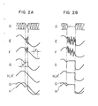
- Fig. 2A shows a plurality of waveforms appearing at various portions of the apparatus shown in Fig. 1.
- a modulated wave D reproduced from a recording medium such as a video tape is applied to the input terminal 1 and then to the detector 2 for detecting the magnitude of the input signal.
- the output signal of the detector 2 is applied to the demodulator 3 thereby to be demodulated and converted into a signal such as an audio signal or a musical signal.
- the demodulated signal is amplified through the amplifier 4 to produce a signal E.
- the phase of the high frequency component of the signal E in the audio frequency band is delayed by a time P through the all-pass circuit 9, thereby generating a signal F.
- the signal F passes through the switch 10, when it is closed, and forms a signal H, which signal H is applied to the amplifier 6 thereby to be amplified.
- a signal H' capable of driving a power amplifier and actuating a loudspeaker is generated at the output terminal 8 of the amplifier 6.
- an end of the holding capacitor 11 is connected to the input terminal to the amplifier 6, and at the same time the output signal E from the amplifier 4 is applied to the same input terminal through the switch 5, when it is closed, and through the resistor 12.
- the all-pass circuit 9 is constructed to have a preselected low output impedance, the output signal E does not have influence on the frequency characteristics of the total signal pass circuit 9 in the audio frequency band.
- the detector 2 detects it and starts its operation and switches off the switches 5 and 10, whereby the dropout noise produced by the demodulator 3 is prevented from being transmitted to the output terminal 8.
- the capacitor 7 connected to the output terminal of the switch 5 functions to hold the output voltage of the amplifier 4 immediately before the occurrence of the dropout noise and the capacitor 11 functions to hold the output voltage of the all-pass circuit 9 immediately before the occurrence of the dropout noise.
- symbols D to H' indicate the signals D to H' appearing at various portions of the apparatus shown in Fig. 1.
- the capacitors 7 and 11 hold respective constant terminal- voltages which have become equal to each other, thereby effecting noise reduction.
- the designation of the symbols D to H' is identical with that of the symbols used in Fig. 2A.
- the waveform of the dropout noise contains a greater number of higher frequency components than the demodulated signal, so that even after passing through the all-pass circuit 9, the dropout noise waveform has only a small amount of time delay as shown in Fig. 2A.
- Fig. 3 designates a capacitor one end of which is connected to an output terminal 8 of the amplifier 6, 15 an amplifier having an input terminal connected to the other end of the capacitor 13, and 14 a resistor connected in parallel with the capacitor 13.
- the amplifier 15 and the capacitor 13 in combination form a differentiating circuit.
- a frequency modulated signal J reproduced through a reproducing circuit (not shown) from a recording medium such as a video tape is applied to an input terminal 1.
- the signal J passes the detector 2 for detecting the magnitude of the signal and is applied to the demodulator 3, where it is demodulated and converted into an audio signal or a musical signal.
- the demodulated signal is amplified through the amplifier 4 to generate an amplified signal K.
- the signal K passes the switch 5, when it is closed, and then it is applied to an input terminal to the amplifier 6, where the signal K is further amplified and delivered to the output terminal 8.
- an output signal L capable of driving a power amplifier and operating a loudspeaker is obtained at the output terminal 8.
- the holding capacitor 7 and the resistor 12 are connected to the input terminal to the amplifier 6, since the output impedance of the amplifier 4 is preset to have a low value and thus there is no influence on the frequency characteristics of the output signal of the amplifier 4 in the audio frequency band.
- the signals recorded on a recording medium such as a video tape can be reproduced and heard by the use of this apparatus.
- the record tracks are not continuous, and thus a discontinuous modulated wave results in the reproduction of the recorded signals. Also, if defects exist in the magnetic tape, a dropout failure occurs in the reproduced modulated wave.
- the demodulator 3 produces noise at the discontinuous portions or the dropout portions of the modulated wave.
- the operation to be performed by the apparatus of this invention shown in Fig. 3 when a dropout occurs in the reproduced modulated wave will be hereinafter described in detail.
- a demodulated output is normally generated at the output terminal 8, as mentioned previously.
- the demodulated output is also applied to the amplifier 15 through the capacitor 13 and the resistor 14.
- the combination of the capacitor 13 and the amplifier 15 forms a differentiating circuit.
- a sum-of the demodulated output supplied through the resistor 14 and a differentiated value of the demodulated output provided by the capacitor 13 is applied to the input to the amplifier 15 and an amplified sum signal is generated at its output.
- the output of the amplifier 15 is supplied through the switch 10, when it is closed, to the capacitor 11 and then to the input terminal to the amplifier 6 through the resistor 12.
- the detector 2 When a dropout occurs in the input reproduced signal J and thereby the level of the modulated wave of the signal J falls, the detector 2 starts its operation and switches off the switches 5 and 10, whereby the noise produced by the demodulator 3 is prevented from being transmitted to the output terminal 8.
- the capacitor 7 functions to hold the output voltage of the amplifier 4 immediately before the occurrence of the dropout noise and the capacitor 11 functions to hold the output voltage of the amplifier 15 immediately before the occurrence of the dropout noise.
- the output voltage of the amplifier 15 contains the differentiated value of the output signal from the amplifier 6, the output voltage of the amplifier 15 becomes higher than the input voltage of the amplifier 6 when the output voltage of the amplifier 6 increases, while, the former becomes lower than the latter when the output voltage of the amplifier 6 decreases.
- the switches 5 and 10 are switched off in response to the occurrence of a dropout, the difference between the respective voltages across the capacitors 7 and 11 indicates the direction of a change of the demodulated output voltage immediately before the occurrence of the dropout. This voltage difference gradually diminishes to zero by virtue of the presence of the bridging resistor 12.
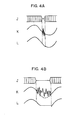
- Fig. 4A The performance waveforms of the apparatus in Fig. 3 is shown in Fig. 4A.
- symbols J, K and L indicate the signals J, K and L at various portions of the apparatus shown in Fig. 3.
- Fig. 4B shows the performance waveforms of the apparatus in Fig. 3 but when the duration of a dropout is long. As will be seen from Figs.
- each of the capacitor 13 and the resistor 14 has its one end connected to the output terminal of the amplifier 6, a similar function may be achieved by connecting one end of each of the capacitor 13 and the resistor 14 to the output terminal of the amplifier 4. In this case, however, the amplification degree decreases by the magnitude of the amplification degree of the amplifier 6, and therefore it becomes necessary to increase the amplification degree of the amplifier 15.
- the present invention can provide a great noise reducing effect because of the fact that, when noise occurs in a demodulated output signal from a demodulator, hold circuits are put into operation and a noise containing portion of the demodulated output signal is replaced by a substitute signal having a waveform close to the original signal waveform containing no noise. Further, since the apparatus of this invention operates to produce a'constant output voltage when the duration of a dropout present in a modulated wave to be demodulated is long, it is possible to prevent noise produced by the demodulator from appearing in the waveform of a demodulated output signal.
Landscapes
- Engineering & Computer Science (AREA)
- Signal Processing (AREA)
- Signal Processing Not Specific To The Method Of Recording And Reproducing (AREA)
- Noise Elimination (AREA)
Applications Claiming Priority (4)
| Application Number | Priority Date | Filing Date | Title |
|---|---|---|---|
| JP80422/84 | 1984-04-20 | ||
| JP59080422A JPS60223307A (ja) | 1984-04-20 | 1984-04-20 | 雑音低減回路 |
| JP59188365A JPS6165627A (ja) | 1984-09-07 | 1984-09-07 | 雑音低減装置 |
| JP188365/84 | 1984-09-07 |
Publications (3)
| Publication Number | Publication Date |
|---|---|
| EP0159042A2 true EP0159042A2 (de) | 1985-10-23 |
| EP0159042A3 EP0159042A3 (en) | 1988-06-08 |
| EP0159042B1 EP0159042B1 (de) | 1991-11-21 |
Family
ID=26421432
Family Applications (1)
| Application Number | Title | Priority Date | Filing Date |
|---|---|---|---|
| EP85104736A Expired - Lifetime EP0159042B1 (de) | 1984-04-20 | 1985-04-19 | Gerät zum Herabsetzen von Geräuschen in Audiosignalen |
Country Status (7)
| Country | Link |
|---|---|
| US (1) | US4648118A (de) |
| EP (1) | EP0159042B1 (de) |
| KR (1) | KR900005064B1 (de) |
| AU (1) | AU562044B2 (de) |
| BR (1) | BR8501854A (de) |
| CA (1) | CA1229799A (de) |
| DE (1) | DE3584686D1 (de) |
Families Citing this family (4)
| Publication number | Priority date | Publication date | Assignee | Title |
|---|---|---|---|---|
| DE3885089T2 (de) * | 1988-04-08 | 1994-05-19 | Hazeltine Corp | Antennensystem mit an Nutz- und Störsignale sich anpassendem Antennendiagramm. |
| US4864561A (en) * | 1988-06-20 | 1989-09-05 | American Telephone And Telegraph Company | Technique for improved subjective performance in a communication system using attenuated noise-fill |
| US5057785A (en) * | 1990-01-23 | 1991-10-15 | International Business Machines Corporation | Method and circuitry to suppress additive disturbances in data channels |
| US5357150A (en) * | 1992-11-06 | 1994-10-18 | International Business Machines Corporation | Defect tolerant envelope follower |
Family Cites Families (16)
| Publication number | Priority date | Publication date | Assignee | Title |
|---|---|---|---|---|
| US3374435A (en) * | 1965-07-29 | 1968-03-19 | Bell Telephone Labor Inc | Reduction of the effect of impulse noise bursts |
| US4184178A (en) * | 1972-11-30 | 1980-01-15 | Basf Aktiengesellschaft | Drop-out compensator for sound reproducing apparatus during tape reversal |
| US4076969A (en) * | 1975-04-07 | 1978-02-28 | Singer & Singer | Impulse noise reduction system |
| JPS5943852B2 (ja) * | 1977-02-08 | 1984-10-25 | 株式会社日立製作所 | 信号ホ−ルド回路 |
| JPS5514734A (en) * | 1978-07-17 | 1980-02-01 | Nec Corp | Pulse noise elimination circuit |
| US4311963A (en) * | 1978-07-18 | 1982-01-19 | Matsushita Electric Industrial Co., Ltd. | Noise pulse suppressing system |
| US4268793A (en) * | 1978-10-12 | 1981-05-19 | Kiyoshi Amazawa | Noise eliminating circuit |
| CA1144081A (en) * | 1979-04-27 | 1983-04-05 | Sadao Kondo | Noise removing apparatus |
| US4329714A (en) * | 1980-11-26 | 1982-05-11 | Rca Corporation | Audio distortion eliminator |
| EP0063737B1 (de) * | 1981-04-23 | 1986-03-19 | TELEFUNKEN Fernseh und Rundfunk GmbH | Videorecorder mit verbesserter Tonwiedergabe |
| JPS581829A (ja) * | 1981-05-06 | 1983-01-07 | Sony Corp | ビデオテ−プレコ−ダ |
| JPS586506A (ja) * | 1981-06-30 | 1983-01-14 | Pioneer Video Corp | 再生信号の時間軸補正装置 |
| JPS58121882A (ja) * | 1982-01-16 | 1983-07-20 | Sony Corp | 映像及び音声信号再生装置 |
| DE3377254D1 (en) * | 1982-07-21 | 1988-08-04 | Victor Company Of Japan | Circuit for reconstructing noise-affected signals |
| US4495643A (en) * | 1983-03-31 | 1985-01-22 | Orban Associates, Inc. | Audio peak limiter using Hilbert transforms |
| DE3929030A1 (de) * | 1989-09-01 | 1991-03-07 | Boehringer Mannheim Gmbh | Verfahren zur vermehrung von nukleinsaeuren |
-
1985
- 1985-04-10 US US06/721,646 patent/US4648118A/en not_active Expired - Fee Related
- 1985-04-11 AU AU41026/85A patent/AU562044B2/en not_active Ceased
- 1985-04-15 CA CA000479194A patent/CA1229799A/en not_active Expired
- 1985-04-16 KR KR1019850002546A patent/KR900005064B1/ko not_active Expired
- 1985-04-18 BR BR8501854A patent/BR8501854A/pt not_active IP Right Cessation
- 1985-04-19 EP EP85104736A patent/EP0159042B1/de not_active Expired - Lifetime
- 1985-04-19 DE DE8585104736T patent/DE3584686D1/de not_active Expired - Lifetime
Also Published As
| Publication number | Publication date |
|---|---|
| DE3584686D1 (de) | 1992-01-02 |
| EP0159042A3 (en) | 1988-06-08 |
| CA1229799A (en) | 1987-12-01 |
| AU4102685A (en) | 1985-10-24 |
| AU562044B2 (en) | 1987-05-28 |
| KR850007515A (ko) | 1985-12-04 |
| EP0159042B1 (de) | 1991-11-21 |
| KR900005064B1 (ko) | 1990-07-19 |
| BR8501854A (pt) | 1985-12-17 |
| US4648118A (en) | 1987-03-03 |
Similar Documents
| Publication | Publication Date | Title |
|---|---|---|
| US4403262A (en) | Audio signal muting circuit for magnetic recording and reproducing apparatus | |
| GB1599807A (en) | Fm signal defect compensation | |
| US4562492A (en) | Noise reduction circuit | |
| US4648118A (en) | Apparatus for reducing noise in audio signals | |
| US5220427A (en) | Magnetic reproducing apparatus having circuit for preventing reversal of white peak | |
| JPH0250522B2 (de) | ||
| US3997914A (en) | Analog encoder decoder circuit | |
| JPS6224474A (ja) | ディジタルオ−ディオディスクプレ−ヤ | |
| JPH0447799Y2 (de) | ||
| JPH0743766Y2 (ja) | Dat装置 | |
| JP2591356B2 (ja) | 記録再生装置 | |
| JPH0337176Y2 (de) | ||
| JPH0442749B2 (de) | ||
| JPS59119511A (ja) | 情報再生装置 | |
| JPH0442750B2 (de) | ||
| JPS6258569B2 (de) | ||
| JPS60223307A (ja) | 雑音低減回路 | |
| JPH0355991A (ja) | エンファシス・ディエンファシス回路 | |
| JPS6165627A (ja) | 雑音低減装置 | |
| JPS59160806A (ja) | ドロツプアウト補償回路 | |
| JPS63129559A (ja) | n倍速録音装置 | |
| JPS62143265A (ja) | 磁気記録再生装置 | |
| JPS60218989A (ja) | サ−チノイズ抑圧回路 | |
| JPS58215711A (ja) | デイジタル信号の再生処理装置 | |
| JPH02216667A (ja) | 白ピーク反転現象補償回路 |
Legal Events
| Date | Code | Title | Description |
|---|---|---|---|
| PUAI | Public reference made under article 153(3) epc to a published international application that has entered the european phase |
Free format text: ORIGINAL CODE: 0009012 |
|
| AK | Designated contracting states |
Designated state(s): DE FR GB NL |
|
| PUAL | Search report despatched |
Free format text: ORIGINAL CODE: 0009013 |
|
| AK | Designated contracting states |
Kind code of ref document: A3 Designated state(s): DE FR GB NL |
|
| 17P | Request for examination filed |
Effective date: 19880720 |
|
| 17Q | First examination report despatched |
Effective date: 19891030 |
|
| GRAA | (expected) grant |
Free format text: ORIGINAL CODE: 0009210 |
|
| AK | Designated contracting states |
Kind code of ref document: B1 Designated state(s): DE FR GB NL |
|
| REF | Corresponds to: |
Ref document number: 3584686 Country of ref document: DE Date of ref document: 19920102 |
|
| ET | Fr: translation filed | ||
| PLBE | No opposition filed within time limit |
Free format text: ORIGINAL CODE: 0009261 |
|
| STAA | Information on the status of an ep patent application or granted ep patent |
Free format text: STATUS: NO OPPOSITION FILED WITHIN TIME LIMIT |
|
| 26N | No opposition filed | ||
| PGFP | Annual fee paid to national office [announced via postgrant information from national office to epo] |
Ref country code: GB Payment date: 19940411 Year of fee payment: 10 Ref country code: FR Payment date: 19940411 Year of fee payment: 10 |
|
| PGFP | Annual fee paid to national office [announced via postgrant information from national office to epo] |
Ref country code: DE Payment date: 19940426 Year of fee payment: 10 |
|
| PGFP | Annual fee paid to national office [announced via postgrant information from national office to epo] |
Ref country code: NL Payment date: 19940430 Year of fee payment: 10 |
|
| PG25 | Lapsed in a contracting state [announced via postgrant information from national office to epo] |
Ref country code: GB Effective date: 19950419 |
|
| PG25 | Lapsed in a contracting state [announced via postgrant information from national office to epo] |
Ref country code: NL Effective date: 19951101 |
|
| GBPC | Gb: european patent ceased through non-payment of renewal fee |
Effective date: 19950419 |
|
| PG25 | Lapsed in a contracting state [announced via postgrant information from national office to epo] |
Ref country code: FR Effective date: 19951229 |
|
| NLV4 | Nl: lapsed or anulled due to non-payment of the annual fee |
Effective date: 19951101 |
|
| PG25 | Lapsed in a contracting state [announced via postgrant information from national office to epo] |
Ref country code: DE Effective date: 19960103 |
|
| REG | Reference to a national code |
Ref country code: FR Ref legal event code: ST |