EP0160789A2 - Générateur de mots numériques de test - Google Patents
Générateur de mots numériques de test Download PDFInfo
- Publication number
- EP0160789A2 EP0160789A2 EP85101567A EP85101567A EP0160789A2 EP 0160789 A2 EP0160789 A2 EP 0160789A2 EP 85101567 A EP85101567 A EP 85101567A EP 85101567 A EP85101567 A EP 85101567A EP 0160789 A2 EP0160789 A2 EP 0160789A2
- Authority
- EP
- European Patent Office
- Prior art keywords
- address
- pattern
- pattern memory
- test
- output
- Prior art date
- Legal status (The legal status is an assumption and is not a legal conclusion. Google has not performed a legal analysis and makes no representation as to the accuracy of the status listed.)
- Granted
Links
Images



Classifications
-
- G—PHYSICS
- G01—MEASURING; TESTING
- G01R—MEASURING ELECTRIC VARIABLES; MEASURING MAGNETIC VARIABLES
- G01R31/00—Arrangements for testing electric properties; Arrangements for locating electric faults; Arrangements for electrical testing characterised by what is being tested not provided for elsewhere
- G01R31/28—Testing of electronic circuits, e.g. by signal tracer
- G01R31/317—Testing of digital circuits
- G01R31/3181—Functional testing
- G01R31/319—Tester hardware, i.e. output processing circuits
- G01R31/31917—Stimuli generation or application of test patterns to the device under test [DUT]
- G01R31/31919—Storing and outputting test patterns
- G01R31/31921—Storing and outputting test patterns using compression techniques, e.g. patterns sequencer
-
- G—PHYSICS
- G01—MEASURING; TESTING
- G01R—MEASURING ELECTRIC VARIABLES; MEASURING MAGNETIC VARIABLES
- G01R31/00—Arrangements for testing electric properties; Arrangements for locating electric faults; Arrangements for electrical testing characterised by what is being tested not provided for elsewhere
- G01R31/28—Testing of electronic circuits, e.g. by signal tracer
- G01R31/317—Testing of digital circuits
- G01R31/3181—Functional testing
- G01R31/319—Tester hardware, i.e. output processing circuits
- G01R31/31903—Tester hardware, i.e. output processing circuits tester configuration
- G01R31/31908—Tester set-up, e.g. configuring the tester to the device under test [DUT], down loading test patterns
Definitions
- the present invention relates to a pattern generator which is employed in testing of logic circuit devices and which generates test data for input into the logic circuit device under test (hereinafter referred to as DUT) and correct data corresponding to the output of the logic circuit device based on the input of the test data, that is, expected value data.
- DUT logic circuit device under test
- flip-flops provided for latching the outputs of respective internal logic circuits in the DUT are arranged to be directly connectable to one another all in series in response to a control signal and individual test patterns are serially input into the series-connected flip-flops. Then the series connection is resolved into individuals and the test data thus input are applied to the subsequent internal or combinatorial logic circuits respectively connected to the flip-flops and the operation of the internal logic circuits is advanced by one clock. The results of their operations are input again into the flip-flops and they are connected again in series, after which their states are serially read out and, at the same time, new test data are serially input into the flip-flops and the read-out data is checked to see whether the corresponding internal logic circuit operated correctly. In this manner, the entire logic circuit device is tested.
- Each of the successive test patterns to be used for the logic circuit device designed by such LSSD techniques is composed of N bits of the same number as the sum of the numbers of input and output terminals of the logic circuit device.
- the test pattern for advancing the operation of the internal logic circuits in parallel i.e.
- the N bit pattern consists of input data and expected value data, but during the periods in which test data is applied to the series-connected flip-flops and operation results are read out from the series connected flip-flops, only three bits in each N-bit test pattern, that is, one-bit test data for input to one end of the series connection of the flip-flops, expected value data for comparison with one-bit data that is read out from the other end of the series connection and one-bit control data for connecting the flip-flops in series, are effectively used, while the other remaining (N-3) bits are not used for test and usually held unchanged.
- N-bit test patterns are prestored at successive addresses of an N-bit-word pattern memory and read out in a sequential order.
- An object of the present invention is to provide a pattern generator which permits a marked reduction of the overall storage capacity of a pattern memory which is used in the case of generating such patterns that differ in part from one another but remain identical in the rest, as described previously.
- test patterns for application to some terminal pins of a logic circuit device under test are stored in a partial pattern memory, which is addressed by an address pointer for readout.
- test patterns each corresponding to a set of all the terminal pins of the DUT increment command patterns for the address pointer and control patterns for controlling whether to enable the output of the partial pattern memory are stored in a main pattern memory, which is read out by an address control circuit.
- the control pattern for enabling the output of the partial pattern memory is ANDed therewith, and the ANDed output is ORed with the corresponding one of the outputs of the main memory read out therefrom for the test patterns applied to the respective terminal pins, thereby providing a test pattern.
- test pattern data for the logic circuit device utilizing the aforesaid LSSD techniques
- input data for the aforementioned series-connected flip-flops and the corresponding expected value data are stored in the partial pattern memory.
- the partial pattern memory has a large depth in the direction of address, but words of a small number of bits can be used.
- the partial pattern memory is read out advancing its address by the address pointer.
- In the main pattern memory are stored at certain intervals such test pattern data each pattern of which includes the aforesaid two bits, which correspond to the series-connection input terminal and the series-connection output terminal of the DUT, respectively, and are each set to a "0".
- this test pattern data includes a control bit which indicates that this data relates to test patterns including the aforesaid two bits.
- the remaining (N-3) bits of the test pattern data are usually the same.
- the number of addresses of the main pattern memory that are needed to be read out is smaller than the number of addresses of the partial pattern memory that are read out.
- the contents of the same address are repeatedly read out of the main pattern memory and the outputs therefrom are respectively ORed with the outputs sequentially read out of different addresses of the partial pattern memory, thus generating new test patterns one after another.
- test patterns which are used for testing a logic circuit device designed by the LSSD techniques.
- N 256 bits.
- a pattern a 1 Stored at an address corresponding to a count value 0 of the program counter is a pattern a 1 which includes test data for application to respective input terminals of the logic circuit under test and, if necessary, expected value data for some combinatorial logic circuits internal to the logic circuit device.
- a pattern b 1 which includes control data for connecting flip-flops (i.e. latches) in the logic circuit device in a series relation to form a scan shift register and data for input into the series connected flip-flops.
- addresses corresponding to count values 2, 3, ... of the program counter are sequentially stored patterns b 21 b 3 , ... of data for input into the series-connected flip-flops.
- a pattern a 2 which includes control data for disconnecting the flip-flops from one another, test data to be applied to the input terminal pins of the logic circuit device and output expected value data to be compared with the outputs from some internal logic circuits.
- patterns b 61 b 7 , ... are sequentially stored which include data to be input into the series-connected flip-flops and expected value data to be compared with the current outputs obtained from the series-connected flip-flops relative to the preceding inputs.
- the input terminal pin to which one end of the series connection is connected is a Pth bit and the output pin having connected thereto the other end is a (P+1)th bit.
- Command data for series connection of the flip-flops is a Oth bit and when this bit is a "1", the flip-flops are connected in series.
- the Oth bit is "1" only the bits P and P+1 in each word of the test patterns b 1 , b 2 , ... are effective data which change in accordance with test data to be eventually generated and the 0th bit is a connection command for the flip-flops.
- the other 253 bits are data which are ignored and usually made identical from pattern to pattern. Since the contents of bits P and P+1 in the patterns b 1 , b 2 , ... change at random, however, they cannot be compressed in a convenient fashion.
- the results of logic operations performed by the internal logic circuits based on the preceding patterns b 1 to b 5 in response to the input of the pattern a 2 are output from the terminal pin P+1 one after another, and at the same time, compared with the corresponding expected value data produced at the bit P+1.
- the series connection of flip-flops also becomes longer, so the memory areas corresponding to the bits 1 to (P-1) and (P+2) to 255 in the respective patterns b . , which are to be ignored during testing, increase extremely. In this respect, it cannot be said that the pattern memory is used efficiently.
- Fig. 2 illustrates an embodiment of the pattern generator of the present invention.
- An address control circuit 11 provides a readout address in common to a test pattern memory 12, an increment command pattern memory 13 and an output enable control pattern memory 14. At the same time, the address control circuit 11 initializes an address pointer 15. The address pointer 15 addresses a partial pattern memory 16.
- the test pattern memory 12 has stored therein test patterns each having a word length corresponding to all terminal pins of a DUT, as shown in Fig. 3. Accordingly, if the number N of the terminal pins of the DUT is 256, then one word is composed of Oth to 255th bits as is the case of Fig. 1, the following test pattern is stored in the pattern memory 12, in addition to the test patterns a 1 , a 21 ...
- a pattern c 1 is used in which only those specific bits of the test pattern, i.e. the bits P and P+1 in the example of Fig. 1, are each given a "0", the Oth bit which provides a command for the series connection of flip-flops in this example is given a "1" and the remainder is made proper data.
- the pattern c 1 is inserted between the test patterns a 1 , a 2 , ... alternately, and such a test pattern array is stored in the pattern memory 12.
- the increment command pattern memory 13 has stored therein data which indicates whether to increment the address pointer 15, that is, data which indicates whether to increment the address of the partial pattern memory 16 for the next readout thereof.
- Each word is one-bit and logic "1" is stored in the case of incrementing the address.
- the output enable control pattern memory 14 has stored therein at each address one-bit data which determines whether to enable the data read out of the partial pattern memory 16.
- the output 14a read from the memory 14 controls a gate circuit 17 to supply it with the output from the partial pattern memory 16.
- logic "1" is stored in the memory 14.
- the output of the gate circuit 17 and the output of the test pattern memory 12 corresponding thereto are ORed by an OR circuit 18.
- the outputs of bits P and P+1 read out of the test pattern memory 12 and two bits read out of the partial pattern memory 16 are ORed with each other.
- the bit positions of the output bits of the test pattern memory 12 which are to be ORed such an arrangement is made that in a pin selector 19, each output of the gate circuit 17 can be switched to any one of bits of the N-bit output of the pin selector 19.
- the partial pattern memory 16 stores in connection with only the patterns b 1 , b 2 , ... in which their some data alone differ from the others.
- the data changing portions of the patterns b 1 to b 5 between the patterns a 1 and a 2 in Fig. 1, that is, data 1a of the bits P and P+1, data 1b of only the data changing portion of the patterns b 2 to b 10 between the patterns a 2 and a3 and similar data of the succeeding patterns are stored in the one-word-two-bit partial pattern memory 16, as depicted in Fig. 4.
- the address of the pattern memory 12 is not updated until the patterns a to a 5 in Fig. 1 have been read out, that is, until the test pattern c 1 having the bits P and P+1 set to "Os" has been repeatedly read out five times in this example, and it is necessary only to update or increment the address of the partial pattern memory 16 sequentially in this while. Accordingly, in the increment command pattern 13 are stored a "1" at each of addresses 1, 3, 5, ... where the pattern c 1 read out of the test pattern memory 12 is stored and a "0" at each of the other addresses 0, 2, 4, ..., as illustrated in Fig. 5.
- the stored contents of the enable control pattern memory 14 are such as shown in Fig. 6 in which a "1" is stored at each of addresses 1, 3, 5, ... where the pattern c 1 is stored and a "0" is stored at each of the other addresses.
- the address 21 of a program counter for reading out the memories 12 to 14 advances from 0 to 1, 1, 1, 1, 1, 1, 2, 3, 3, ..., as shown in Fig. 7.
- the address control circuit 11 sets a 0 in the address pointer 15 to set it to 0, as shown.
- the address 21 of the program counter is initially set to a 0, as mentioned above, and a "0" is produced as each of the outputs 13a and 14a of the memories 13 and 14, and further, a "0" is produced as the output 15a of the address pointer 15 by the initialization.
- the increment command pattern memory 13 yields a "1"
- the address pointer 15 is incremented.
- the output 14a of the enable control pattern memory 14 is a "1”
- the output of the partial pattern memory 16 read out of an address specified by the address pointer 15 is provided via the gate circuit 17 to the OR circuit 18, wherein it is O Red with each of the bits P and P+1 of the test pattern c 1 read out of the test pattern memory 12, thus producing the test pattern b 1 ,
- step 2 since the increment command previously issued from the increment command pattern memory 13 is a "1", the address pointer 15 is incremented by one and its output 15a goes to a "1". As a result, an address 1 of the partial pattern memory 16 is read out, and at this time, the output 14a of the enable control pattern memory 14 is a "1" and the output of the partial pattern memory 16 is ORed with the output of the test pattern memory 12, outputting the test pattern b 2 . Until step 5 the address 21 remains at "1" and similar operations are repeated. As the process advances step by step in this while, the output 15a of the address pointer 15 is incremented one by one.
- step 6 the address 21 goes to a "2", and the memories 12, 13 and 14 output the pattern a 2 , an increment command pattern "0" and an output enable control pattern "0", respectively. Since the increment command in the preceding step 5 was a “1”, however, the output 15a of the address pointer 15 has been incremented to a "5". Since the output enable control pattern output 14a is a "0”, the output of the gate circuit 17 goes to a "0”, and in the test pattern memory 12 an address 2 is specified, from which the pattern a 2 is read out and output as a test pattern. In step 7 the address 21 goes to a "3" and the pattern c 1 is read out.
- the output 15a of the address pointer 15 holds the previous value "5" and the partial pattern memory 16 is read out at the address being specified by the address pointer 15.
- the output enable control pattern output 14a is a "1" and it is provided via the gate circuit 17 to the OR circuit 18, wherein it is ORed with the pattern c 1 read out of the test pattern memory 12, and the ORed output is provided as the test pattern b 6 . In the succeeding steps similar operations are carried out.
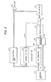
- the address control circuit 11 in Fig. 2 may be, for instance, such as described in U.S. Patent No. 4,313,200 (issued on January 20, 1982); that is, it is formed as a microprogram control system, as depicted in Fig. 8.
- the count value of a program counter 31 is output as the address 21 from the address control circuit 11, and by this address 21, an operation code part 32 and an operand part 33 are read out in addition to the contents of the memories 12, 13 and 14.
- the memories 12, 13 and 14, the operation code part 32 and the operand part 33 make up together a main pattern memory 34.
- An instruction read out of the operation code part 32 is decoded in an instruction decoder 35, performing address control in accordance with the contents of the instruction.
- Connected to the instruction decoder 35 are an index counter 36 and a subroutine stack 37.
- Instructions loaded in the operation code part 32 are a no operation instruction NOP for simply incrementing the program counter 31 by one, a loop instruction, a subroutine execute instruction JSR and a return instruction RTN.
- the loop instruction is to inhibit the increment of the program counter 31 the number of times of clocks equal to a value loaded in the operand part 33. That is, when this instruction is read out of the operation code part 32 and judged to be the loop instruction in the instruction decoder 35, the value of an operand simultaneously read out of the operand part 33 is loaded into the index counter 36, and for each step (clock), the content of the index counter 36 is decremented while the increment of the program counter is stopped. When the index counter 36 has been decremented to zero, the program counter 31 is incremented by one.
- the loop instruction is read out of the operation code part 32, and at the same time, the value indicating the number of looping operations, 5, is read out of the operand part 33. Accordingly, the program counter 31 is held at the same address 21 in the course of five steps, after which the address 21 of the program counter 31 advances by one. In this manner, the aforesaid operation is carried out.
- the subroutine execute instruction JSR is to advance the execution to an address which is read out of the operand part 33 at the same time as the instruction JSR and to advance the program counter 31 by one upon completion of the execution.
- the instruction decode part 35 when it is judged in the instruction decode part 35 that the readout instruction is the subroutine execute instruction JSR, the value that the contents of the program counter 31 at that time has been incremented by one is loaded into the subroutine stack 37, after which a value read out of the operand part 33 at the same time is preset in the program counter 31 and then the subroutine is executed.
- the operation code part 32 has loaded therein the return instruction RTN, and when the instruction RTN is read out, the instruction decode part 35 sets in the program counter 31 the value loaded in the subroutine stack 37.
- the output 13a of the increment command pattern memory 13 is read into a D flip-flop 39 by a clock which is applied from a terminal 38 for each step, and the output of the flip-flop 39 is supplied to an enable terminal E of a counter 41.
- the counter 41 advances by one for each application of the clock from the terminal 38.
- a "0" is being applied to the terminal E, even if the clock is provided from the terminal 38, the counter 41 does not advance.
- the count value of the counter 41 is provided as the output 15a of the address pointer 15.
- the counter 41 is presettable and, it can be set to an initial value via the line 22 from the address control circuit 11, as described previously in respect of Fig. 2.
- the pin selector 19 in Fig. 2 is formed, for example, as illustrated in Fig. 10.
- the gate circuit 17 is to yield two bits in this example, and it is made up of gate circuits 17 1 and 17 2 , the outputs of which are connected to selectors 19 0 to 19 255 of the pin selector 19.
- the selectors 19 0 to 19 255 respectively have inhibit terminals 42 0 to 42 255 and select terminals 43 0 to 43 255 .
- each selector When an inhibit command is being applied to the inhibit terminal, each selector does not yield an output, but when no inhibit command is applied to the inhibit terminal, it selectively passes therethrough one of the outputs of the gate circuits 17 1 and 17 2 in accordance with a select command supplied to the select terminal.
- the outputs of the selectors 19 0 to 19 255 are each provided to the one input of each of OR circuits 18 0 to 18 255 of the OR circuit 1 8, and the other inputs of the OR circuits 18 0 to 18 255 are respectively supplied with bits 0 to 255 read out of the test pattern memory 12. Accordingly, by selecting the commands which are provided to the inhibit terminals 42 0 to 42 255 and the select terminals 43 0 to 43 255 of the pin selector 19, the output of the gate circuit 17 1 can be supplied to any of the OR circuits 18 0 to 18 255 and, similarly, the output of the gate circuit 17 2 can also be applied to any of the OR circuits 18 0 to 18255.
- the output 13a of the increment command pattern memory 13 is to determine whether or not to increment the address pointer 15 and the output 14a of the enable control pattern memory 14 is to determine whether or not to enable data read out of the partial pattern memory 14, so they differ in function.
- the stored contents of the increment command pattern memory 13 and the stored contents of the enable control pattern memory 14 are exactly the same. Therefore, it is also possible to interconnect the output sides of these memories 13 and 14 and to omit one of them.
- the test pattern memory 12 stores test patterns each including a control data bit (e.g. Oth bit in Fig.
- a sequence of the command data bits exactly correspond to either of the sequence of enable control patterns and the sequence of increment command patterns. Therefore, it is also possible to omit both the increment command pattern memory 13 and the enable control pattern memory 14, and to arrange such that the Oth bit output of the test pattern memory 12 is used as the enable control patterns 14a and also as the increment command patterns 13a, that is, the Oth bit output of the memory 12 is connected to the gate circuit 17 and the address pointer 15.
- the increment command pattern memory 13 and the enable control pattern memory 14 are generically called an auxiliary pattern memory and the patterns stored in them are called auxiliary patterns.
- the increment command pattern memory 13 and the enable control pattern memory 14 which are one-bit-word memories accessable with the address 21 common to the test pattern memory 12, so these memories 12, 13 and 14 can be constituted as one memory. That is to say, by using such a memory in which one word is composed of bits whose number is larger than that of the terminal pins of the DUT by two or more and by storing a sequence of the enable control patterns and a sequence of the increment command patterns in the corresponding two bit positions at successive addresses, the memories 12, 13 and 14 can be formed as one memory.
- the partial pattern memory 16 may be a two-bit word memory in this example, even if its depth is great in an address direction, a small storage capacity is enough as a whole.
- there may be only very few memory cells (i.e. bits) in total which do not serve to generate successive test patterns and the entire area of the memory 12 can be utilized effectively to store data for generation of a long sequence of test patterns, enabling the test pattern data necessary for a complete test to be transferred from a pattern file to the memory 12 through one continuous transfer operation.
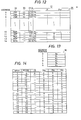
- the present invention is applicable not only to the case of generating test patterns for the logic circuit devices using the LSSD techniques, as described previously, but also to the case where the same sequence of steps for generating test patterns is repeated but data of only some corresponding bits in the corresponding patterns in the respective sequences are modified as shown in Fig. 11, for instance.
- one process i.e. a test is made using a sequence of test patterns a 0 to a 5 , but data of the corresponding Pth to P+nth bits in the corresponding test patterns a 2 , a and a 4 are modified for the respective tests.
- test pattern is stored in the test pattern memory for each step, as shown in Fig. 11. Accordingly, a number of similar test patterns are stored in the test pattern memory.
- test patterns 10, 11, 12, 13 and 14 are respectively stored test patterns a 1 , a 2 ', a 3 1 , a 4 ' and a 5 in the test pattern memory 12, "0", “1” “0” “1” and “0” in the increment command pattern memory 13, "0", “1", “1”, “1” and “0” in the enable control pattern memory 14 and NOP, NOP, NOP, NOP and RTN in the operation code part 32.
- the P to P+nth bits of the test patterns a 2 , a3 and a 4 are all "Os".
- step 1 the address 21 of the program counter 31 is a "0"
- the output of each of the memories 13 and 14 is a "0”
- the output a of the test pattern memory 12 is provided as a test pattern.
- a value "1" obtained by adding "1" to the current content of the program counter 31 is loaded into the subroutine stack 37 and then, the operand 10 read out from the operand area 33 at that time is set in the program counter 31.
- step 2 the contents at the address "10" designated by the program counter 31 are read out to initiate the subroutine. Since the output read out of the memory 14 at this time is a "0", the output a 1 of the test pattern memory 12 is provided as a test pattern. Then, the NOP instruction advances the counter 31 by one address.
- step 3 the stored contents of the address "11" are read out, and since the output of the memory 14 is a, "1" at this time, the output a 2 ' of the test pattern memory 12 is ORed with the data d 0 read out of the partial pattern memory 16 at the address 0, outputting the test pattern a 2 . Then, the program counter 31 is incremented by the NOP instruction, and at the same time the address pointer 15 is incremented by the output "1" from the memory 13. In step 4 the address "12" of the main pattern memory 34 is read out.
- step 5 the address "13" of the main pattern memory 34 is read out.
- the output a 4 ' of the memory 12 is ORed with the output d 1 from the same address of the memory 16 as that read out in the previous step, providing the test pattern a4.
- step 6 the address 14 of the main pattern memory 34 is read out. Since the output of the memory 14 is "0", the output a 5 from the memory 12 is output as the test pattern a . Further, since the output of the operation code part 32 is the return instruction RTN, the value 1 which has been held in the subroutine stack 37 is set in the program counter 31. Consequently, in step 7 the address 1 of the main pattern memory 34 is read out and the test pattern a is output in the same manner as in step 0, after which the process proceeds to the subroutine, repeating the same operations as described above.
- addresses of the test pattern memory 12 are assigned to all of the test patterns to be generated, but in the examples of Figs. 12 and 13, it is necessary only to assign five addresses to the subroutine and to store the data dot d1, d 2 , ... in the (n+1) bit-word partial pattern memory 16, and consequently, the storage capacity required is extremely reduced.
- each of the data d 1 , d 3 , d 5 ... is repeated in the successive test patterns a3 and a4 in the respective sequences a 0 to a 5 ; this is because the same data has to be applied during two cycles (usually a plurality of cycles) in the test of a microcomputer, for example.
- the changing bit data in the patterns are stored in a partial pattern memory and bits of the corresponding patterns in a pattern memory are each set to a "0", by which the repetitive patterns of exactly the same test pattern are produced at those portions.
- This enables compression of the repetitive patterns, and hence permits an extremely effective use of the pattern memory and the generation of a long sequence of test patterns with a small storage capacity. Accordingly, even if the sequence of test patterns is very long, the number of its split transfers from the pattern file to the test pattern memory can be decreased smaller than has been needed in the past, reducing the entire time for testing.
Landscapes
- Engineering & Computer Science (AREA)
- General Engineering & Computer Science (AREA)
- Physics & Mathematics (AREA)
- General Physics & Mathematics (AREA)
- Tests Of Electronic Circuits (AREA)
- Test And Diagnosis Of Digital Computers (AREA)
Applications Claiming Priority (2)
| Application Number | Priority Date | Filing Date | Title |
|---|---|---|---|
| JP59027643A JPH0641966B2 (ja) | 1984-02-15 | 1984-02-15 | パタ−ン発生装置 |
| JP27643/84 | 1984-02-27 |
Publications (3)
| Publication Number | Publication Date |
|---|---|
| EP0160789A2 true EP0160789A2 (fr) | 1985-11-13 |
| EP0160789A3 EP0160789A3 (en) | 1988-09-28 |
| EP0160789B1 EP0160789B1 (fr) | 1991-07-03 |
Family
ID=12226609
Family Applications (1)
| Application Number | Title | Priority Date | Filing Date |
|---|---|---|---|
| EP85101567A Expired - Lifetime EP0160789B1 (fr) | 1984-02-15 | 1985-02-13 | Générateur de mots numériques de test |
Country Status (4)
| Country | Link |
|---|---|
| US (1) | US4670879A (fr) |
| EP (1) | EP0160789B1 (fr) |
| JP (1) | JPH0641966B2 (fr) |
| DE (1) | DE3583357D1 (fr) |
Cited By (3)
| Publication number | Priority date | Publication date | Assignee | Title |
|---|---|---|---|---|
| DE3900248A1 (de) * | 1988-01-06 | 1989-07-27 | Teradyne Inc | Steuersystem fuer einen automatischen schaltungstester |
| DE3934237A1 (de) * | 1989-10-13 | 1990-02-15 | Peter Dipl Ing Schiwek | Wiederbefuellbare spruehdose, die mit druckluft betrieben wird |
| WO1999014611A1 (fr) * | 1997-09-16 | 1999-03-25 | Teradyne, Inc. | Systeme d'essai pour circuit integre utilisant une memoire unique pour le mode d'essai en parallele et le mode d'essai en balayage |
Families Citing this family (17)
| Publication number | Priority date | Publication date | Assignee | Title |
|---|---|---|---|---|
| DE3676377D1 (de) * | 1985-01-31 | 1991-02-07 | Hitachi Ltd | Generator fuer testmuster. |
| JPH0750159B2 (ja) * | 1985-10-11 | 1995-05-31 | 株式会社日立製作所 | テストパタ−ン発生装置 |
| JPS62195572A (ja) * | 1986-02-21 | 1987-08-28 | Mitsubishi Electric Corp | 半導体テスト装置 |
| CA1259680A (fr) * | 1986-05-06 | 1989-09-19 | Mosaid Technologies Inc. | Brouilleur de signaux numeriques |
| EP0255118B1 (fr) * | 1986-07-30 | 1999-06-09 | Hitachi, Ltd. | Générateur de configurations |
| US4857774A (en) * | 1986-09-19 | 1989-08-15 | Actel Corporation | Testing apparatus and diagnostic method for use with programmable interconnect architecture |
| JP2609284B2 (ja) * | 1988-05-10 | 1997-05-14 | 株式会社日立製作所 | 分散形タイミング信号発生装置 |
| JPH0812230B2 (ja) * | 1988-09-06 | 1996-02-07 | 株式会社日立製作所 | Ic試験装置 |
| JPH0255331U (fr) * | 1988-10-11 | 1990-04-20 | ||
| US5285453A (en) * | 1990-12-28 | 1994-02-08 | International Business Machines Corporation | Test pattern generator for testing embedded arrays |
| JP2602997B2 (ja) * | 1991-01-18 | 1997-04-23 | 株式会社東芝 | パターン発生器 |
| DE69322446D1 (de) * | 1992-07-21 | 1999-01-21 | Advanced Micro Devices Inc | Modulator-Prüfsysteme |
| US5717695A (en) * | 1995-12-04 | 1998-02-10 | Silicon Graphics, Inc. | Output pin for selectively outputting one of a plurality of signals internal to a semiconductor chip according to a programmable register for diagnostics |
| KR100238933B1 (ko) * | 1996-01-12 | 2000-03-02 | 오우라 히로시 | 시험 패턴 발생기 |
| US6032275A (en) * | 1996-01-12 | 2000-02-29 | Advantest Corp. | Test pattern generator |
| WO1998023968A1 (fr) * | 1996-11-29 | 1998-06-04 | Advantest Corporation | Generateur de configuration |
| US6154865A (en) * | 1998-11-13 | 2000-11-28 | Credence Systems Corporation | Instruction processing pattern generator controlling an integrated circuit tester |
Family Cites Families (13)
| Publication number | Priority date | Publication date | Assignee | Title |
|---|---|---|---|---|
| US3783254A (en) * | 1972-10-16 | 1974-01-01 | Ibm | Level sensitive logic system |
| US3873818A (en) * | 1973-10-29 | 1975-03-25 | Ibm | Electronic tester for testing devices having a high circuit density |
| JPS5247344A (en) * | 1975-10-13 | 1977-04-15 | Advantest Corp | Pattern generating equipment |
| JPS5360122A (en) * | 1976-11-10 | 1978-05-30 | Nippon Telegr & Teleph Corp <Ntt> | Test pattern generator |
| US4313200A (en) * | 1978-08-28 | 1982-01-26 | Takeda Riken Kogyo Kabushikikaisha | Logic test system permitting test pattern changes without dummy cycles |
| JPS5585265A (en) * | 1978-12-23 | 1980-06-27 | Toshiba Corp | Function test evaluation device for integrated circuit |
| FR2498849B1 (fr) * | 1981-01-26 | 1986-04-25 | Commissariat Energie Atomique | Generateur de signaux logiques combines |
| JPS5861629A (ja) * | 1981-10-09 | 1983-04-12 | Hitachi Ltd | ビツトパタ−ン発生装置 |
| JPS58137058A (ja) * | 1982-02-06 | 1983-08-15 | Hitachi Ltd | テストパタ−ン自動生成方法および装置 |
| JPS58148977A (ja) * | 1982-03-02 | 1983-09-05 | Nec Corp | 論理回路試験方式 |
| JPS5994086A (ja) * | 1982-11-19 | 1984-05-30 | Advantest Corp | 論理回路試験装置 |
| US4571724A (en) * | 1983-03-23 | 1986-02-18 | Data I/O Corporation | System for testing digital logic devices |
| US4550406A (en) * | 1983-06-14 | 1985-10-29 | Everett/Charles Test Equipment, Inc. | Automatic test program list generation using programmed digital computer |
-
1984
- 1984-02-15 JP JP59027643A patent/JPH0641966B2/ja not_active Expired - Lifetime
-
1985
- 1985-02-13 EP EP85101567A patent/EP0160789B1/fr not_active Expired - Lifetime
- 1985-02-13 DE DE8585101567T patent/DE3583357D1/de not_active Expired - Lifetime
- 1985-02-15 US US06/702,256 patent/US4670879A/en not_active Expired - Lifetime
Cited By (4)
| Publication number | Priority date | Publication date | Assignee | Title |
|---|---|---|---|---|
| DE3900248A1 (de) * | 1988-01-06 | 1989-07-27 | Teradyne Inc | Steuersystem fuer einen automatischen schaltungstester |
| DE3934237A1 (de) * | 1989-10-13 | 1990-02-15 | Peter Dipl Ing Schiwek | Wiederbefuellbare spruehdose, die mit druckluft betrieben wird |
| WO1999014611A1 (fr) * | 1997-09-16 | 1999-03-25 | Teradyne, Inc. | Systeme d'essai pour circuit integre utilisant une memoire unique pour le mode d'essai en parallele et le mode d'essai en balayage |
| US6049901A (en) * | 1997-09-16 | 2000-04-11 | Stock; Mary C. | Test system for integrated circuits using a single memory for both the parallel and scan modes of testing |
Also Published As
| Publication number | Publication date |
|---|---|
| DE3583357D1 (de) | 1991-08-08 |
| EP0160789A3 (en) | 1988-09-28 |
| US4670879A (en) | 1987-06-02 |
| EP0160789B1 (fr) | 1991-07-03 |
| JPH0641966B2 (ja) | 1994-06-01 |
| JPS60170771A (ja) | 1985-09-04 |
Similar Documents
| Publication | Publication Date | Title |
|---|---|---|
| US4670879A (en) | Pattern generator | |
| US4404519A (en) | Testing embedded arrays in large scale integrated circuits | |
| EP0031431B1 (fr) | Réseau logique séquentiel programmable | |
| KR970004074B1 (ko) | 메모리 장치 및 이를 포함한 집적 회로 | |
| US4597042A (en) | Device for loading and reading strings of latches in a data processing system | |
| KR0148621B1 (ko) | 반도체 메모리 시험장치 | |
| US4402081A (en) | Semiconductor memory test pattern generating apparatus | |
| EP0114304A1 (fr) | Assistance matérielle et méthode de traitement de vecteur | |
| US4300234A (en) | Address pattern generator for testing a memory | |
| EP0042222A2 (fr) | Générateur de séquence programmable pour test digital "en circuit" | |
| EP0222084B1 (fr) | Système de test à architecture hiérarchique | |
| US3996566A (en) | Shift and rotate circuit for a data processor | |
| EP0180196A2 (fr) | Dispositif compteur/temporisateur programmable | |
| JPS58108475A (ja) | テストベクトルのシーケンスを発生する装置 | |
| US4586181A (en) | Test pattern generating apparatus | |
| US5285453A (en) | Test pattern generator for testing embedded arrays | |
| US5606568A (en) | Method and apparatus for performing serial and parallel scan testing on an integrated circuit | |
| US5673274A (en) | Test method for semiconductor device | |
| US4696005A (en) | Apparatus for reducing test data storage requirements for high speed VLSI circuit testing | |
| EP0211087A1 (fr) | Generateur de configurations de controle | |
| EP0040219B1 (fr) | Processeur de donnees ayant des moyens communs de controle et de charge et de verification de memoire | |
| EP0553080B1 (fr) | Appareil d'essai à grande fréquence et méthode pour fournir des boucles successives des signaux de données à une fréquence d'horloge prédéterminée | |
| US6567942B1 (en) | Method and apparatus to reduce the size of programmable array built-in self-test engines | |
| EP0141562B1 (fr) | Méthode et dispositif pour la génération d'une séquence de mots à plusieurs bits | |
| US6321352B1 (en) | Integrated circuit tester having a disk drive per channel |
Legal Events
| Date | Code | Title | Description |
|---|---|---|---|
| PUAI | Public reference made under article 153(3) epc to a published international application that has entered the european phase |
Free format text: ORIGINAL CODE: 0009012 |
|
| 17P | Request for examination filed |
Effective date: 19850213 |
|
| AK | Designated contracting states |
Designated state(s): DE GB NL |
|
| PUAL | Search report despatched |
Free format text: ORIGINAL CODE: 0009013 |
|
| AK | Designated contracting states |
Kind code of ref document: A3 Designated state(s): DE GB NL |
|
| 17Q | First examination report despatched |
Effective date: 19900426 |
|
| GRAA | (expected) grant |
Free format text: ORIGINAL CODE: 0009210 |
|
| AK | Designated contracting states |
Kind code of ref document: B1 Designated state(s): DE GB NL |
|
| REF | Corresponds to: |
Ref document number: 3583357 Country of ref document: DE Date of ref document: 19910808 |
|
| PLBE | No opposition filed within time limit |
Free format text: ORIGINAL CODE: 0009261 |
|
| STAA | Information on the status of an ep patent application or granted ep patent |
Free format text: STATUS: NO OPPOSITION FILED WITHIN TIME LIMIT |
|
| 26N | No opposition filed | ||
| PGFP | Annual fee paid to national office [announced via postgrant information from national office to epo] |
Ref country code: GB Payment date: 19940203 Year of fee payment: 10 |
|
| PGFP | Annual fee paid to national office [announced via postgrant information from national office to epo] |
Ref country code: NL Payment date: 19940228 Year of fee payment: 10 |
|
| PG25 | Lapsed in a contracting state [announced via postgrant information from national office to epo] |
Ref country code: GB Effective date: 19950213 |
|
| PG25 | Lapsed in a contracting state [announced via postgrant information from national office to epo] |
Ref country code: NL Effective date: 19950901 |
|
| GBPC | Gb: european patent ceased through non-payment of renewal fee |
Effective date: 19950213 |
|
| NLV4 | Nl: lapsed or anulled due to non-payment of the annual fee |
Effective date: 19950901 |
|
| PGFP | Annual fee paid to national office [announced via postgrant information from national office to epo] |
Ref country code: DE Payment date: 20040226 Year of fee payment: 20 |