EP0162706B1 - Folie aus polymerisiertem Kunststoff mit leitendem Muster und Verfahren zur Herstellung derselben - Google Patents
Folie aus polymerisiertem Kunststoff mit leitendem Muster und Verfahren zur Herstellung derselben Download PDFInfo
- Publication number
- EP0162706B1 EP0162706B1 EP19850303589 EP85303589A EP0162706B1 EP 0162706 B1 EP0162706 B1 EP 0162706B1 EP 19850303589 EP19850303589 EP 19850303589 EP 85303589 A EP85303589 A EP 85303589A EP 0162706 B1 EP0162706 B1 EP 0162706B1
- Authority
- EP
- European Patent Office
- Prior art keywords
- film
- pattern
- electrically conductive
- polymer
- electrode
- Prior art date
- Legal status (The legal status is an assumption and is not a legal conclusion. Google has not performed a legal analysis and makes no representation as to the accuracy of the status listed.)
- Expired - Lifetime
Links
Images


Classifications
-
- H—ELECTRICITY
- H05—ELECTRIC TECHNIQUES NOT OTHERWISE PROVIDED FOR
- H05K—PRINTED CIRCUITS; CASINGS OR CONSTRUCTIONAL DETAILS OF ELECTRIC APPARATUS; MANUFACTURE OF ASSEMBLAGES OF ELECTRICAL COMPONENTS
- H05K3/00—Apparatus or processes for manufacturing printed circuits
- H05K3/10—Apparatus or processes for manufacturing printed circuits in which conductive material is applied to the insulating support in such a manner as to form the desired conductive pattern
- H05K3/105—Apparatus or processes for manufacturing printed circuits in which conductive material is applied to the insulating support in such a manner as to form the desired conductive pattern by conversion of non-conductive material on or in the support into conductive material, e.g. by using an energy beam
-
- H—ELECTRICITY
- H05—ELECTRIC TECHNIQUES NOT OTHERWISE PROVIDED FOR
- H05K—PRINTED CIRCUITS; CASINGS OR CONSTRUCTIONAL DETAILS OF ELECTRIC APPARATUS; MANUFACTURE OF ASSEMBLAGES OF ELECTRICAL COMPONENTS
- H05K3/00—Apparatus or processes for manufacturing printed circuits
- H05K3/10—Apparatus or processes for manufacturing printed circuits in which conductive material is applied to the insulating support in such a manner as to form the desired conductive pattern
-
- H—ELECTRICITY
- H05—ELECTRIC TECHNIQUES NOT OTHERWISE PROVIDED FOR
- H05K—PRINTED CIRCUITS; CASINGS OR CONSTRUCTIONAL DETAILS OF ELECTRIC APPARATUS; MANUFACTURE OF ASSEMBLAGES OF ELECTRICAL COMPONENTS
- H05K2201/00—Indexing scheme relating to printed circuits covered by H05K1/00
- H05K2201/03—Conductive materials
- H05K2201/032—Materials
- H05K2201/0329—Intrinsically conductive polymer [ICP]; Semiconductive polymer
-
- Y—GENERAL TAGGING OF NEW TECHNOLOGICAL DEVELOPMENTS; GENERAL TAGGING OF CROSS-SECTIONAL TECHNOLOGIES SPANNING OVER SEVERAL SECTIONS OF THE IPC; TECHNICAL SUBJECTS COVERED BY FORMER USPC CROSS-REFERENCE ART COLLECTIONS [XRACs] AND DIGESTS
- Y10—TECHNICAL SUBJECTS COVERED BY FORMER USPC
- Y10S—TECHNICAL SUBJECTS COVERED BY FORMER USPC CROSS-REFERENCE ART COLLECTIONS [XRACs] AND DIGESTS
- Y10S428/00—Stock material or miscellaneous articles
- Y10S428/901—Printed circuit
-
- Y—GENERAL TAGGING OF NEW TECHNOLOGICAL DEVELOPMENTS; GENERAL TAGGING OF CROSS-SECTIONAL TECHNOLOGIES SPANNING OVER SEVERAL SECTIONS OF THE IPC; TECHNICAL SUBJECTS COVERED BY FORMER USPC CROSS-REFERENCE ART COLLECTIONS [XRACs] AND DIGESTS
- Y10—TECHNICAL SUBJECTS COVERED BY FORMER USPC
- Y10T—TECHNICAL SUBJECTS COVERED BY FORMER US CLASSIFICATION
- Y10T428/00—Stock material or miscellaneous articles
- Y10T428/24—Structurally defined web or sheet [e.g., overall dimension, etc.]
- Y10T428/24802—Discontinuous or differential coating, impregnation or bond [e.g., artwork, printing, retouched photograph, etc.]
- Y10T428/24851—Intermediate layer is discontinuous or differential
- Y10T428/24868—Translucent outer layer
- Y10T428/24876—Intermediate layer contains particulate material [e.g., pigment, etc.]
-
- Y—GENERAL TAGGING OF NEW TECHNOLOGICAL DEVELOPMENTS; GENERAL TAGGING OF CROSS-SECTIONAL TECHNOLOGIES SPANNING OVER SEVERAL SECTIONS OF THE IPC; TECHNICAL SUBJECTS COVERED BY FORMER USPC CROSS-REFERENCE ART COLLECTIONS [XRACs] AND DIGESTS
- Y10—TECHNICAL SUBJECTS COVERED BY FORMER USPC
- Y10T—TECHNICAL SUBJECTS COVERED BY FORMER US CLASSIFICATION
- Y10T428/00—Stock material or miscellaneous articles
- Y10T428/24—Structurally defined web or sheet [e.g., overall dimension, etc.]
- Y10T428/24802—Discontinuous or differential coating, impregnation or bond [e.g., artwork, printing, retouched photograph, etc.]
- Y10T428/24893—Discontinuous or differential coating, impregnation or bond [e.g., artwork, printing, retouched photograph, etc.] including particulate material
- Y10T428/24901—Discontinuous or differential coating, impregnation or bond [e.g., artwork, printing, retouched photograph, etc.] including particulate material including coloring matter
-
- Y—GENERAL TAGGING OF NEW TECHNOLOGICAL DEVELOPMENTS; GENERAL TAGGING OF CROSS-SECTIONAL TECHNOLOGIES SPANNING OVER SEVERAL SECTIONS OF THE IPC; TECHNICAL SUBJECTS COVERED BY FORMER USPC CROSS-REFERENCE ART COLLECTIONS [XRACs] AND DIGESTS
- Y10—TECHNICAL SUBJECTS COVERED BY FORMER USPC
- Y10T—TECHNICAL SUBJECTS COVERED BY FORMER US CLASSIFICATION
- Y10T428/00—Stock material or miscellaneous articles
- Y10T428/25—Web or sheet containing structurally defined element or component and including a second component containing structurally defined particles
-
- Y—GENERAL TAGGING OF NEW TECHNOLOGICAL DEVELOPMENTS; GENERAL TAGGING OF CROSS-SECTIONAL TECHNOLOGIES SPANNING OVER SEVERAL SECTIONS OF THE IPC; TECHNICAL SUBJECTS COVERED BY FORMER USPC CROSS-REFERENCE ART COLLECTIONS [XRACs] AND DIGESTS
- Y10—TECHNICAL SUBJECTS COVERED BY FORMER USPC
- Y10T—TECHNICAL SUBJECTS COVERED BY FORMER US CLASSIFICATION
- Y10T428/00—Stock material or miscellaneous articles
- Y10T428/31504—Composite [nonstructural laminate]
- Y10T428/31507—Of polycarbonate
-
- Y—GENERAL TAGGING OF NEW TECHNOLOGICAL DEVELOPMENTS; GENERAL TAGGING OF CROSS-SECTIONAL TECHNOLOGIES SPANNING OVER SEVERAL SECTIONS OF THE IPC; TECHNICAL SUBJECTS COVERED BY FORMER USPC CROSS-REFERENCE ART COLLECTIONS [XRACs] AND DIGESTS
- Y10—TECHNICAL SUBJECTS COVERED BY FORMER USPC
- Y10T—TECHNICAL SUBJECTS COVERED BY FORMER US CLASSIFICATION
- Y10T428/00—Stock material or miscellaneous articles
- Y10T428/31504—Composite [nonstructural laminate]
- Y10T428/31533—Of polythioether
-
- Y—GENERAL TAGGING OF NEW TECHNOLOGICAL DEVELOPMENTS; GENERAL TAGGING OF CROSS-SECTIONAL TECHNOLOGIES SPANNING OVER SEVERAL SECTIONS OF THE IPC; TECHNICAL SUBJECTS COVERED BY FORMER USPC CROSS-REFERENCE ART COLLECTIONS [XRACs] AND DIGESTS
- Y10—TECHNICAL SUBJECTS COVERED BY FORMER USPC
- Y10T—TECHNICAL SUBJECTS COVERED BY FORMER US CLASSIFICATION
- Y10T428/00—Stock material or miscellaneous articles
- Y10T428/31504—Composite [nonstructural laminate]
- Y10T428/3154—Of fluorinated addition polymer from unsaturated monomers
-
- Y—GENERAL TAGGING OF NEW TECHNOLOGICAL DEVELOPMENTS; GENERAL TAGGING OF CROSS-SECTIONAL TECHNOLOGIES SPANNING OVER SEVERAL SECTIONS OF THE IPC; TECHNICAL SUBJECTS COVERED BY FORMER USPC CROSS-REFERENCE ART COLLECTIONS [XRACs] AND DIGESTS
- Y10—TECHNICAL SUBJECTS COVERED BY FORMER USPC
- Y10T—TECHNICAL SUBJECTS COVERED BY FORMER US CLASSIFICATION
- Y10T428/00—Stock material or miscellaneous articles
- Y10T428/31504—Composite [nonstructural laminate]
- Y10T428/31678—Of metal
- Y10T428/31688—Next to aldehyde or ketone condensation product
-
- Y—GENERAL TAGGING OF NEW TECHNOLOGICAL DEVELOPMENTS; GENERAL TAGGING OF CROSS-SECTIONAL TECHNOLOGIES SPANNING OVER SEVERAL SECTIONS OF THE IPC; TECHNICAL SUBJECTS COVERED BY FORMER USPC CROSS-REFERENCE ART COLLECTIONS [XRACs] AND DIGESTS
- Y10—TECHNICAL SUBJECTS COVERED BY FORMER USPC
- Y10T—TECHNICAL SUBJECTS COVERED BY FORMER US CLASSIFICATION
- Y10T428/00—Stock material or miscellaneous articles
- Y10T428/31504—Composite [nonstructural laminate]
- Y10T428/31678—Of metal
- Y10T428/31692—Next to addition polymer from unsaturated monomers
-
- Y—GENERAL TAGGING OF NEW TECHNOLOGICAL DEVELOPMENTS; GENERAL TAGGING OF CROSS-SECTIONAL TECHNOLOGIES SPANNING OVER SEVERAL SECTIONS OF THE IPC; TECHNICAL SUBJECTS COVERED BY FORMER USPC CROSS-REFERENCE ART COLLECTIONS [XRACs] AND DIGESTS
- Y10—TECHNICAL SUBJECTS COVERED BY FORMER USPC
- Y10T—TECHNICAL SUBJECTS COVERED BY FORMER US CLASSIFICATION
- Y10T428/00—Stock material or miscellaneous articles
- Y10T428/31504—Composite [nonstructural laminate]
- Y10T428/31721—Of polyimide
-
- Y—GENERAL TAGGING OF NEW TECHNOLOGICAL DEVELOPMENTS; GENERAL TAGGING OF CROSS-SECTIONAL TECHNOLOGIES SPANNING OVER SEVERAL SECTIONS OF THE IPC; TECHNICAL SUBJECTS COVERED BY FORMER USPC CROSS-REFERENCE ART COLLECTIONS [XRACs] AND DIGESTS
- Y10—TECHNICAL SUBJECTS COVERED BY FORMER USPC
- Y10T—TECHNICAL SUBJECTS COVERED BY FORMER US CLASSIFICATION
- Y10T428/00—Stock material or miscellaneous articles
- Y10T428/31504—Composite [nonstructural laminate]
- Y10T428/31855—Of addition polymer from unsaturated monomers
- Y10T428/31935—Ester, halide or nitrile of addition polymer
-
- Y—GENERAL TAGGING OF NEW TECHNOLOGICAL DEVELOPMENTS; GENERAL TAGGING OF CROSS-SECTIONAL TECHNOLOGIES SPANNING OVER SEVERAL SECTIONS OF THE IPC; TECHNICAL SUBJECTS COVERED BY FORMER USPC CROSS-REFERENCE ART COLLECTIONS [XRACs] AND DIGESTS
- Y10—TECHNICAL SUBJECTS COVERED BY FORMER USPC
- Y10T—TECHNICAL SUBJECTS COVERED BY FORMER US CLASSIFICATION
- Y10T428/00—Stock material or miscellaneous articles
- Y10T428/31504—Composite [nonstructural laminate]
- Y10T428/31942—Of aldehyde or ketone condensation product
-
- Y—GENERAL TAGGING OF NEW TECHNOLOGICAL DEVELOPMENTS; GENERAL TAGGING OF CROSS-SECTIONAL TECHNOLOGIES SPANNING OVER SEVERAL SECTIONS OF THE IPC; TECHNICAL SUBJECTS COVERED BY FORMER USPC CROSS-REFERENCE ART COLLECTIONS [XRACs] AND DIGESTS
- Y10—TECHNICAL SUBJECTS COVERED BY FORMER USPC
- Y10T—TECHNICAL SUBJECTS COVERED BY FORMER US CLASSIFICATION
- Y10T428/00—Stock material or miscellaneous articles
- Y10T428/31504—Composite [nonstructural laminate]
- Y10T428/31971—Of carbohydrate
Definitions
- the present invention relates to a polymer film with a conductive pattern and a method of manufacturing the same.
- EP-A-0140304 discloses a method for producing electrically-conductive paths in crystalline poly (arylene sulphide) by subjecting areas of the polymer pattern-wise to heat or solvent treatment to render it amorphous in those areas, and then relying upon the differential receptivity of the amorphous material to dopants in solution, to render the amorphous areas conductive by a doping treatment.
- a polymer film containing a conductive pattern characterized in that it comprises a film of an insulating polymer which includes pattern areas defined by the presence of an electrically conductive polymer of an aromatic compound, rendered electrically conductive by in situ polymerization, and non-pattern areas defined by the absence of the said conductive polymer, the conductive pattern having an internal portion extending into the thickness of the film from at least one major surface of said film.
- a method of manufacturing an insulating polymer film which has an electrically conductive pattern therein characterized by the steps of:-
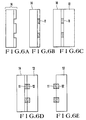
- Figs. 1A to 1D are respectively sectional views illustrating particular steps in manufacturing a polymer film with a conductive pattern according to the present invention
- Fig. 2 is a sectional view showing a polymer film with a conductive pattern according to another embodiment of the present invention
- Figs. 3A to 3C are respectively sectional views which illustrate particular steps in manufacturing a polymer film with a conductive pattern according to still another embodiment of the present invention.
- Figs. 4 and 5 are sectional views showing polymer films with conductive patterns according to other embodiments of the present invention, respectively;
- Figs. 6A to 6F are respectively sectional views which illustrate particular steps in creating the pattern of Fig.5;
- Figs. 7A to 7D are respectively sectional views illustrating particular steps in manufacturing a polymer film with a conductive pattern according to still another embodiment of the present invention.
- Fig. 8 is a plan view of the polymer film with the conductive pattern prepared by the steps in Fig. 1.
- Figs. 1A to 1D show a polymer film with a conductive pattern of the present invention and the principle of the method of manufacturing the same.
- reference numeral 1 denotes an insulating substrate; 3, an electrically conductive layer formed on the entire surface of the insulating substrate 1; 4, an insulating pattern; 5, a polymer film; 6, an electrically conductive portion; and 7, an insulating portion.
- Figs. 3A to 3C are respectively sectional views for explaining the steps in manufacturing a polymer film with a conductive pattern according to still another embodiment of the present invention.
- Figs. 4 and 5 are sectional views showing polymer films with conductive patterns according to other embodiments of the present invention, respectively;
- Figs. 6A to 6F are respectively sectional views for explaining the steps in manufacturing the pattern of Fig. 5;
- Figs. 7A to 7D are respectively sectional views for explaining the steps in manufacturing a polymer film with a conductive pattern according to still another embodiment of the present invention.
- Fig. 8 is a plan view of the polymer film with the conductive pattern prepared by the steps in Fig. 1.
- Figs. 1A to 1D show a polymer film with a conductive pattern of the present invention and the principle of the method of manufacturing the same.
- reference numeral 1 denotes an insulating substrate; 3, an electrically conductive layer formed on the entire surface of the insulating substrate 1; 4, an insulating pattern; 5, a polymer film; 6, an electrically conductive portion; and 7, an insulating portion.
- the electrically conductive layer 3 is formed on the insulating substrate 1.
- the insulating layer 4 with a desired pattern is formed by lithography on the electrically conductive layer 3.
- the insulating substrate 1, the electrically conductive layer 3 and the insulating pattern 4 constitute an electrode substrate 10.
- the electrically conductive layer comprises a metal (e.g., gold, platinum, palladium, chromium or titanium) or an electrically conductive metal oxide (e.g., tin oxide or indium oxide) or semiconductor.
- the insulating pattern 4 comprises a resist film, an insulating oxide (e.g., SiO or SiO2 ) or a nitride (e.g., Si3N4 or BN).
- the insulated polymer film 5 is coated on the electrode substrate 10 by a proper method such as casting, spin coating or a doctor blade method.
- the insulated polymer film used in the present invention is selected from a polyvinyl chloride resin (i.e., polyvinyl chloride or a copolymer of vinyl chloride with other vinyl monomer), a polyvinylidene chloride resin (i.e., polyvinylidene chloride or a copolymer of vinylidene chloride with other vinyl monomer), a polyvinylidene fluoride resin (i.e., polyvinylidene fluoride or a copolymer of vinylidene fluoride with other vinyl monomer), a polystyrene resin (i.e., polystyrene or a copolymer of styrene with other vinyl monomer), an acrylic resin (i.e., polymethylacrylate or a copolymer of other acrylic monomer with other vinyl monomer), polyvinyl carbazole, a copolymer of vinyl carbazole with other vinyl monomer, a copolymer of ethylene with other vinyl
- Additives such as a plasticizer, a heat stabilizer, a lubricant, an ultraviolet absorber, a defogging agent, a pigment, a dye, a surfactant, an electrically conductive filler and the like may be added to the polymer materials described above.
- An aromatic compound subjected to electrochemical polymerization can be selected from the group consisting of pyrrole, 3-methylpyrrole, N-methylpyrrole, thiophene, furan, phenol, thiophenol, selenophene, tellurophene, biphenyl, azulene, p-terphenyl, o-terphenyl, p-quaterphenyl, 2-hydroxybiphenyl, diphenylsulfide, 2-( ⁇ -thienyl)thiophene, 2-( ⁇ -thienyl)furan, 2-(2-pyrrolyl)pyrrole, 2-(2-pyrrolyl)thiophene, 2-phenylthiophene, ⁇ -thienylphenyl ether, ⁇ -furyl- ⁇ -thienylselenide, 2-(2-pyrrolyl)selenophene, 2-(2-selenienyl)tellurophene, N-vinylcarbazole, N
- a compound such as an organic quaternary ammonium salt, protonic acid or an inorganic salt is used as an electrolyte in electrochemical polymerization.
- a solvent for dissolving an aromatic compound to be electrochemically polymerized an acetonitrile, benzonitrile, or propylene carbonate based solution is normally used and the solvent composition is adjusted in accordance with the type of insulated polymer film to be rendered electrically conductive. This selection must be made such that an aromatic compound and electrolytic anions are diffused in the film to progress polymerization without dissolving the insulated polymer film.
- the polymer film is peeled to obtain a polymer film having a desired electrically conductive pattern.
- an insulating polymer film portion which contacts the electrically conductive portion of the electrode is made conductive.
- Another insulating polymer film portion which contacts the insulating portion of the electrode is kept insulative.
- the entire film can be easily peeled from the electrode.
- the electrode can be repeatedly used.
- the film with a conductive pattern can be continuously formed at low cost.
- both major surfaces or one major surface (the surface contacting the electrode surface) of the film can be made conductive in accordance with polymerization conditions.
- the type of pattern, an insulating film material, a structure of the electrically conductive film can be modified to provide a virtually indefinite number of combinations.
- the electrically conductive pattern is formed entirely from the upper surface to the lower surface of the film along the direction of thickness thereof.
- this conductive pattern can be formed from one surface of the film to a certain depth. Therefore, the present invention is not limited to the following examples.
- a 1,000-A indium oxide film was sputtered on a glass substrate.
- a one-dimensional grating pattern was formed on the electrically conductive substrate having the indium oxide layer thereon in the following manner.
- a 2- ⁇ m photoresist AZ-1350J (Shipley Corp.) was spin coated on the indium oxide layer and was exposed with a photomask having a one-dimensional grating pattern with 0.1-mm wide stripes separated by 0.1-mm wide spaces.
- a 2,000-A SiO film was deposited to the exposed photoresist film and was lifted off in methyl ethyl ketone to prepare an SiO pattern as an insulating layer having a 0.1-mm width at 0.2-mm pitches on the indium oxide layer.
- Casting was performed using a solution of polyvinyl chloride (molecular weight: 700,000) in methyl ethyl ketone to obtain a 20- ⁇ m film on the substrate.
- the substrate with the film was dipped in an electrolytic solution obtained by dissolving 0.3 mol/l of tetraethylammonium paratoluenesulfonate and 1 mol/l of pyrrole in an acetonitrile-methyl ethyl ketone (1 : 1) solvent mixture.
- a titanium mesh plated with platinum was used as the counter electrode.
- Electrochemical polymerization of pyrrole was performed at a voltage of 3.0 V for 10 minutes, thereby precipitating black polypyrrole.
- Example 2 An electrical conductivity of the film was measured to be as high as 4.5 S/cm along a direction parallel to the stripes of the electrode. However, a portion of the film had an insulating property of 10 ⁇ 13 S/cm or less in a direction perpendicular to the stripes. As a result, an electrically insulated film with high anisotropy was prepared.
- Example 2 An electrical conductivity of the film was measured to be as high as 4.5 S/cm along a direction parallel to the stripes of the electrode. However, a portion of the film had an insulating property of 10 ⁇ 13 S/cm or less in a direction perpendicular to the stripes. As a result, an electrically insulated film with high anisotropy was prepared.
- Example 2 An electrical conductivity of the film was measured to be as high as 4.5 S/cm along a direction parallel to the stripes of the electrode. However, a portion of the film had an insulating property of 10 ⁇ 13 S/cm or less in a direction perpendicular to the
- a 500- ⁇ ITO indium-tin oxide
- a 2- ⁇ m photoresist AZ-1350J (Shipley Corp.) was spin coated on the ITO layer and was exposed with a photomask having a two-dimensional grating pattern having 50- ⁇ m pitches. The exposed photoresist film was developed, and then a 2,000- ⁇ silicon oxide (SiO) film was deposited thereon. The lift-off was performed in the methyl ethyl ketone solution.
- a two-dimensional pattern of the SiO layer as the insulating layer was formed on the electrically conductive ITO layer. Conductive island regions at an interval of 50 ⁇ m were formed on the surface of the ITO layer.
- a 15- ⁇ m vinylidene chloride-vinyl chloride (75 : 25) copolymer film was coated by casting on the substrate. The substrate with the film was dipped in an acetonitrile-tetrohydrofuran (2 : 1) solution containing thiophene (1 mol/l) and tetraethylammonium perchlorate (0.3 mol/l).
- a titanium mesh electrode plated with platinum was also dipped in this solution to perform electrochemical polymerization of thiophene at a voltage of 4.0 V for 10 minutes.
- green polythiophene was precipitated, and its film was peeled from the electrode substrate.
- An electrical conductivity of a portion as the upper surface of the film was 10 ⁇ 12 S/cm or less and regarded as an insulating property.
- An electrical conductivity of the film along the direction of thickness thereof was as high as 1.5 S/cm. As a result, a film having conductivity only along the direction of thickness was prepared.
- An electrode resistance is one of the polymerization parameters.
- an electrode substrate having a low resistance the two major surfaces of the film can be easily made conductive.
- an electrode substrate having a high resistance only one major surface described above can be easily made conductive.
- a lower surface of the film which contacts the electrode surface is entirely made conductive.
- only the low-resistance portion is made conductive.
- a 2,000- ⁇ ITO layer was deposited thereon.
- a 2- ⁇ m photoresist AZ-1350J was spin coated on the ITO layer and was exposed with a photomask to form a one-dimensional stripe pattern having stripes of 50 ⁇ m separated by spaces of 50 ⁇ m.
- the photoresist film was then developed, and the ITO layer was etched for 1,200 ⁇ in a parallel-plate type reactive ion etching apparatus using an etchant of CBrF3 at a flow rate of 20 SCCM, a pressure of 20 mTorr and a power of 100 W.
- an electrode substrate was prepared wherein ITO oxide layers having thickness of 800 ⁇ and 2,000 ⁇ ware alternately formed on the gold layer at intervals of 50 ⁇ m.
- a 20- ⁇ m polyvinyl chloride (molecular weight: 70,000) film was formed by casting on the resultant electrode substrate. Electrochemical polymerization of pyrrole was performed for the electrode with the film in the same manner as in Example 2. Polypyrrole was precipitated on the entire surface of the film. The polypyrrole film could be easily peeled from the electrode substrate. A surface of the film which contacted the electrode substrate had a high electrical conductivity of 12 S/cm in a direction parallel to the one-dimensional stripe pattern and a high electrical conductivity of 8.5 S/cm in a direction perpendicular thereto.
- a surface of the polypyrrole film which contacted the electrolytic solution had a high conductivity of 6.8 S/cm in a direction parallel to the stripes but had an insulation of 10 ⁇ 12 S/cm or less in the direction perpendicular thereto.
- the electrically conductive patterns having different resistivities were formed on the electrode surfaces and the electrochemical polymerization conditions were properly selected, one surface was made entirely conductive, and the other surface had an anisotropic conductivity pattern.
- a polymer film is coated on an electrode with a desired electrically conductive pattern, and an aromatic compound is electrochemically polymerized to obtain a polymer film having the same pattern as the electrically conductive pattern of the electrode, thereby easily manufacturing a film having anisotropic conductivity or a special electrically conductive pattern.
- the resultant films can be used in a variety of applications for components much, as patterned electrically conductive layers of two-dimensional input devices, input terminals of display elements and output terminals of image sensors.
- the electrically conductive pattern constituting the electrode substrate 10 is obtained such that the insulated pattern 4 is formed on the electrically conductive layer 3.
- an electrically conductive pattern 2 may be directly formed on an insulating substrate 1.
- the electrode with the conductive pattern described above may comprise a drum-like structure for continuously forming a polymer film with a conductive pattern.
- a simplified electrode structure for forming a film with a conductive pattern will be described hereinafter.
- a material such as a semi-insulating semiconductor material is used wherein a high electrical resistance is given in a dark state without light exposure but the surface resistance is decreased, so that a portion subjected to light exposure can be made conductive. Therefore, the portion subjected to light exposure is limited to obtain a polymer film having a desired conductive pattern.
- an insulated polymer film 26 is coated on a major surface of a semi-insulating semiconductor substrate 25 serving as an electrode substrate.
- a current required for electrochemical polymerization flows in only the exposed portion, thereby obtaining an electrically conductive area 28 (indicated by hatched lines) in the polymer film 26.
- the polymer film 26 is peeled from the electrode to prepare a polymer film with a conductive pattern shown in Fig. 3C.
- the flat surface of the electrode can be used, and the patterning of electrode substrate is not necessary.
- the resultant film can be easily peeled from the electrode, because of no pattern on the electrode.
- the amorphous silicon film had a resistivity of about 108 ⁇ cm in a dark state.
- 1- ⁇ m polyvinyl chloride was spin coated on the amorphous silicon film.
- An insulating rubber resin was coated on a surface of the stainless steel plate which did not have the amorphous silicon film thereon.
- the resultant substrate was dipped together with a platinum counter electrode in an electrolytic solution obtained by dissolving 0.3 mol/l of tetraethylammonium paratoluenesulfonate and 1 mol/l of pyrrole in an acetonitrile-tetrahydrofuran (2 : 1) solvent mixture.
- a voltage of 1.2 V was applied between the film coated with the polyvinyl chloride film and the platinum counter electrode.
- a polypyrrole was formed in the irradiated area, and a polymer film having the polypyrrole or conductive pattern was obtained.
- the resultant film was peeled from the amorphous silicon substrate.
- An electrical conductivity of the film was measured by-a 4-terminal method in a direction parallel to the polypyrrole stripes to obtain a high conductivity of 10 S/cm.
- an electrical conductivity of the film was measured in a direction perpendicular to the polypyrrole stripes, an insulating property was given as 10 ⁇ 8 S/cm or more.
- amorphous silicon film was deposited on a stainless steel plate, polyvinyl chloride was coated on the amorphous silicon film with a thickness of about 1 ⁇ m, and an insulating rubber resin was coated on a surface of the stainless steel plate which did not have the amorphous silicon film thereon, thereby obtaining a substrate in the same manner as in Example 4.
- a photomask having a stripe pattern with a 50- ⁇ m width and a 200- ⁇ m pitch was brought into contact with the polyvinyl chloride coated on the substrate.
- the substrate with the photomask was dipped together with a platinum counter electrode in an electrolytic solution obtained by dissolving 0.3 mol/l of tetraethylammonium paratoluenesulfonate and 1 mol/l of pyrrole in an acetonitrile-tetrahydrofuran (2 : 1) solvent mixture.
- a voltage of 1.6 V was applied between the film coated with the polyvinyl chloride film and the platinum counter electrode.
- the resultant film was peeled from the amorphous silicon substrate.
- An electrical conductivity of the film was measured to be as high as 20 S/cm by a 4-terminal method in a direction parallel to the polypyrrole stripes. However, when an electrical conductivity of the film was measured in a direction perpendicular to the polypyrrole stripes, an insulating property was given as 10 ⁇ 8 S/cm or more.
- a polymer film was coated on a substrate whose electrical resistance is decreased upon light exposure, and light irradiates the film in a desired pattern.
- the exposed portion is used as an electrode, and electrochemical polymerization is performed, thereby easily preparing a film having anisotropic conductivity or a special conductive circuit pattern.
- the film with the conductive pattern described above comprises a hybrid structure of an insulating polymer and an electrically conductive polymer, so that the electrical conductivity is degraded as compared with the electrochemical polymer.
- an electrically conductive pattern becomes narrow, its electrical resistance is increased. In this sense, a range of applications of the film is often limited.
- an electrically conductive portion is obtained by laminating an electrically conductive layer made of an electrochemically polymerized aromatic compound and a layer obtained by mixing an electrochemically polymerized aromatic compound in an insulating polymer film.
- Figs. 6A to 6F are sectional views for explaining the steps in manufacturing a polymer film having an electrically conductive pattern.
- an electrode substrate 14 is dipped together with a counter electrode in an electrochemical polymerization solution of an aromatic compound.
- a DC voltage is applied between the electrode substrate 14 and the counter electrode.
- An electrochemical polymer layer 11 of an aromatic compound is formed in correspondence with the conductive electrode pattern (Fig. 6B).
- the electrode substrate 14 shown in Fig. 6A is constituted by the insulating substrate of Fig. 1A, the electrically conductive layer formed thereon and the insulating pattern formed on the electrically conductive layer.
- the electrode substrate may be constituted by the electrically conductive layer directly formed on the insulating substrate.
- an insulating polymer film 13 is formed on the electrode substrate (Fig. 6C).
- the electrode substrate with the film is dipped in an electrochemical polymerization solution again to perform electrochemical polymerization of an aromatic compound.
- An electrochemical polymer is grown from an insulating polymer film portion contacting the single electrochemical polymer layer formed in the electrically conductive pattern of the electrode substrate and is formed in the insulating polymer film, thereby obtaining an electrically conductive polymer layer 12 (Fig. 6D).
- a film with an electrically conductive pattern is formed on only one major surface, as shown in Fig. 5.
- Figs. 4 and 5 show a polymer film structure having an electrically conductive pattern of the present invention.
- An electrically conductive pattern comprises a laminate of a single electrochemical polymer layer 11 of an aromatic compound and an electrically conductive polymer layer 12 obtained by combining the insulating polymer film material and the electrochemical polymer, and the electrically conductive pattern is formed in the insulating polymer film 13.
- the single electrochemical polymer layer 11 decreases a surface resistance of the electrically conductive pattern
- the polymer layer 12 increases adhesion strength between the single electrochemical polymer layer and the insulating polymer film and increases the thickness of the electrically conductive pattern.
- the insulating polymer film holds the electrically conductive pattern and increases the mechanical strength of the film.
- the polymer layer 12 comprises a layer which is entirely conductive as shown in Fig. 4 or a layer whose one surface is made conductive as shown in Fig. 5. Either type of polymer layer 12 can be used for a desired application.
- a chromium layer of 15 nm was deposited on a glass substrate having an ITO layer and a surface resistance of 10 ⁇ to prepare an electrode substrate.
- a 3.5- ⁇ m SiO2 film was sputtered on the substrate.
- a 2- ⁇ m photoresist AZ-1350 (Shipley Corp.) was spin coated on the SiO2 film.
- the photoresist layer was exposed and developed to obtain a photoresist pattern.
- the SiO, film was etching by plasma etching using CF4 gas as an etchant and the photoresist pattern as a mask.
- the photoresist pattern was then removed to form SiO2 stripes on the chromium-ITO surface.
- the SiO2 stripes had a width of 10 ⁇ m and formed at a rate of 50 stripes per millimeter.
- a solution of pyrrole (1 mol/l) and tetraethylammonium paratoluenesulfonate (0.3 mol/l) in acetonitrile-nitrobenzene (4 : 1) was prepared as an electrochemical polymerization solution.
- the resultant electrode substrate as an anode and a platinum-plated titanium mesh electrode as a cathode were dipped in the above solution.
- a DC voltage of 2 V was applied between the cathode and the anode while a charge density was kept at 0.6 coulomb/cm2, thereby performing electrochemical polymerization of pyrrole and hence obtaining polypyrrole having a thickness of 2 ⁇ m and not covered with SiO2 .
- a methyl ethyl ketone solution of polyvinyl chloride (molecular weight: 70,000) was casted on the polypyrrole film having a thickness of 2 ⁇ m, thereby forming a polyvinyl chloride film having a thickness of 20 ⁇ m.
- the electrode substrate with the film was dipped together with a platinum-plated titanium mesh electrode in the electrolytic solution of pyrrole.
- a DC voltage of 1.5 V was then applied between the electrode substrate and the mesh electrode while a charge density of 0.15 coulomb/cm2 was kept to perform pyrrole polymerization.
- the film after polymerization was washed with ethanol and dried. The dried film was peeled from the electrode substrate.
- the polypyrrole film which was first obtained was not left on the electrode substrate.
- the polyvinyl chloride film was strongly adhered with the patterned polypyrrole film. Upon peeling of the film, surface resistances of a surface (to be referred to as an electrode contact surface) of the film which contacted the electrode along the direction parallel to the stripes and perpendicular thereto were measured by a 4-terminal method. The surface resistances of the film along the parallel and vertical directions were 15 ⁇ and 20 M ⁇ or more, respectively.
- a polyvinyl chloride film having a thickness of 20 ⁇ m was directly formed on the electrode substrate used in the above embodiment. Electrochemical polymerization of pyrrole was performed on the electrode with the film at a voltage of 1.5 V and a charge density of 0.15 coulomb/cm2. The surface resistances of the film along directions parallel to and perpendicular to the stripes were 3.5 k ⁇ and 20 M ⁇ , respectively.
- a platinum film having a thickness of 20 nm was deposited on a glass substrate having a surface resistance of 10 ⁇ and an ITO layer.
- a 3- ⁇ m photoresist AZ-1350J (Shipley Corp.) was spin coated on the platinum film.
- the photoresist film was exposed by using a photomask having a one-dimensional pattern having a stripe width of 40 ⁇ m and a space of 10 ⁇ m between the adjacent stripes and was developed to obtain a photoresist pattern.
- a 2- ⁇ m SiO film was deposited to cover the entire surface of the substrate and was lifted off in methyl ethyl ketone, thereby obtaining a 50-stripes/mm SiO pattern having a stripe width of 10 ⁇ m.
- An acetonitrile solution of thiophene (0.8 mol/l) and tetraethylammonium perchlorate (0.2 mol/l) was prepared as an electrochemical polymerization solution.
- the electrode substrate as an anode and a platinum-plated titanium mesh electrode as a cathode were dipped in the above solution.
- a DC voltage of 5 V was applied between the anode and the cathode while a charge density of 0.7 coulomb/cm2 was kept to electrochemically polymerize thiophene, thereby forming a 1.8- ⁇ m polythiophene film on the platinum/ITO pattern.
- a cyclohexanone solution of polyvinylidene chloride was casted on the substrate to form a 30- ⁇ m polyvinylidene chloride film.
- the resultant electrode substrate with the film was dipped together with a platinum-plating titanium mesh electrode in the electrolytic solution of thiophene.
- a DC voltage of 3 V was applied between the electrode substrate and the mesh electrode while a charge density of 0.2 coulomb/cm2 was kept to perform polymerization of thiophene.
- the film was washed with ethanol and dried. The dried film was peeled from the electrode substrate.
- the polythiophene film first formed was not left between the patterns on the electrode substrate.
- the polyvinylidene chloride film was strongly adhered with the polythiophene film.
- the peeled film was subjected to surface resistance measurement by a 4-terminal method. Surface resistances of the film along directions parallel and perpendicular to the stripes and the vertical direction were 130 ⁇ and 20 M ⁇ or more, respectively.
- a polyvinylidene chloride film having a thickness of 30 ⁇ m was formed directly on the same electrode substrate as this Example.
- thiophene was electrochemically polymerized at a voltage of 3 V and a charge density of 0.2 coulomb/cm2.
- the surface resistances of the resultant film along directions parallel and perpendicular to the stripes were measured to be 6.5 k ⁇ and 20 M ⁇ or more, respectively.
- the polymer film with a conductive pattern was formed thereon to decrease the surface resistance of the patterned electrically conductive film to about 1/10.
- An acetonitrile-nitrobenzene (4 : 1) solution of pyrrole (1 mol/l) and tetraethylammonium tetrafluoroborate (0.3 mol/l) was prepared as an electrochemical polymerization solution.
- An electrode substrate as an anode and a platinum-plated titanium mesh electrode as a cathode in the same manner as in Example 1 were dipped in the above solution A DC voltage of 2 V was applied between the anode and the cathode while a charge density of 0.6 coulomb/cm3 was kept to electrochemically polymerize pyrrole, thereby forming a 2- ⁇ m polypyrrole layer on the conductive portion on the electrode substrate.
- a tetrahydrofuran solution of polystyrene (molecular weight: 800,000) was casted on the surface of the substrate to obtain a polystyrene film having a thickness of 4.5 ⁇ m.
- the resultant substrate with the film was dipped together with a platinum-plated titanium mesh electrode in an electrolytic solution of pyrrole.
- a DC voltage of 1.5 V was applied between the electrode substrate and the titanium mesh electrode while a charge density of 0.3 coulomb/cm2 was kept to electrochemically polymerize pyrrole.
- the film was washed with ethanol and dried. The dried film was peeled from the electrode.
- the polypyrrole film first formed on the electrode was not left between the patterns on the electrode substrate.
- the polystyrene film was strongly adhered with the patterned polypyrrole film. After peeling of the film, the surface resistances of the electrode contact surface of the film along directions parallel and perpendicular to the pattern were measured by the 4-terminal method to be 10 ⁇ and 20 M ⁇ , respectively.
- a polystyrene film having a thickness of 15 ⁇ m was formed directly on the same electrode substrate as in this Example. Pyrrole was electrochemically polymerized on the electrode substrate with the film at a voltage of 1.5 V and a charge density of 0.3 coulomb/cm2 to form a polymer film with a conductive pattern. The surface resistances of the electrode contact surface of the film along directions parallel and perpendicular to the pattern were measured to be 280 ⁇ and 20 M ⁇ or more, respectively.
- the polymer film with a conductive pattern was formed thereon, thereby-decreasing the surface resistance of the patterned electrically conductive film to about 1/10.
- a gold film having a thickness of 15 nm was deposited on a glass substrate having a surface resistance of 10 ⁇ and an ITO layer to prepare an electrode substrate.
- An SiO2 film was sputtered on the electrode substrate to a thickness of 5 ⁇ m.
- a 3- ⁇ m photoresist AZ-1350J (Shipley Corp.) was spin coated on the SiO2 film.
- the photoresist film was exposed with a photomask having a circular pattern with a diameter of 50 ⁇ m at lateral and vertical intervals of 200 ⁇ m and was developed to obtain a photoresist pattern.
- the SiO2 film was plasma etched by using the photoresist pattern as a mask and CF4 gas as an etchant. After the photoresist pattern was removed, an SiO2 layer having apertures each having the diameter of 50 ⁇ m was formed on the surface of the gold-ITO surface.
- An acetonitrile-ethanol (4 : 1) solution of pyrrole (1 mol/l) and tetraethylammonium paratoluenesulfonate (0.3 mol/l) was prepared as an electrochemical polymerization solution.
- the electrode substrate as an anode and a platinum-plated titanium mesh electrode as a cathode were dipped in the solution.
- a DC voltage of 5 V was applied between the anode and the cathode while a charge density of 3 coulomb/cm2 was kept to electrochemically polymerize pyrrole, thereby forming a 9- ⁇ m polypyrrole film on the electrode substrate.
- a dimethylformamide solution of polyvinylidene fluoride (molecular weight: 120,000) was casted on the electrode substrate to form a polyvinylidene fluoride film having a thickness of 12 ⁇ m.
- the substrate with the film was dipped together with a platinum-plated titanium mesh electrode in the electrolytic solution of pyrrole.
- a DC voltage of 3 V was applied between the electrode substrate and the mesh electrode while a charge density of 0.8 coulomb/cm2 was kept to electrochemically polymerize pyrrole.
- the film was washed with ethanol and dried. The dried film was peeled from the electrode. In this case, the polypyrrole film first formed in a circular shape on the electrode was not left on the electrode.
- the polyvinylidene fluoride film was strongly adhered to the polypyrrole film. After peeling of the film, resistances of the surfaces of the film which contacted the electrode and the solution and the resistance of the film along a direction of thickness of the film were measured by the 4-terminal method. The surface resistances were 20 M ⁇ or more, and the resistance along the thickness direction were 25 ⁇ , respectively. The film having conductivity only along the thickness direction was prepared.
- a polyvinylidene fluoride film having a thickness of 12 ⁇ m was directly formed on the same electrode substrate as in this Example. Pyrrole was electrochemically polymerized on the electrode substrate with the film at a voltage of 5 V and a charge density of 4 coulomb/cm2 to prepare a polymer film with a conductive pattern.
- the surface resistances of the film which contacted the electrode and the solution and the resistance along the direction of thickness of the film were measured by the 4-terminal method.
- the surface resistances of the two surfaces were 20 M ⁇ or more, and the resistance along the thickness of the film were 55 ⁇ . In this manner, the resultant film had conductivity only along the thickness direction.
- the polymer film with a conductive pattern was formed thereon.
- the resistance along the thickness direction can be decreased to about 1/10, thereby obtaining the film having conductivity only along the thickness direction.
- an electrochemical polymer layer of an aromatic compound was formed on the electrode having a predetermined electrically conductive pattern, and then an insulating polymer film was formed thereon to electrochemically polymerize the aromatic compound, thereby forming the insulating polymer film-electrochemically polymer layer.
- a polymer film having a low electrical resistance was prepared.
- Figs. 7A to 7D show still another embodiment of the present invention.
- reference numeral 30 denotes an insulating substrate; 31, an electrically conductive layer for constituting an electrode; 32, an insulating pattern; 33, an insulating polymer film; and 34, a conductive polymer film.
- Fig. 8 shows an electrode pattern having regular linear conductive portions.
- the insulating pattern 32 is formed on the surface of the low-resistance electrode 31 formed on the insulating substrate 30 to leave linear gaps.
- the polymer film 33 is formed on the surface of the resultant structure, as shown in Fig. 7B.
- the gaps In order to obtain uniform electrical conductivity and uniform transmittance along a film surface, the gaps must be uniformly and regularly formed.
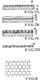
- a hexagonal or honneycomb structure (Fig. 8) or an octagonal structure is preferred.
- the gap width is less than 10 ⁇ m and more preferably 5 ⁇ m or less.
- the pitch between the gaps preferably corresponds to the thickness of the polymer film to be made conductive. Unless the pitch is at least 20 ⁇ m or more, a sufficiently high transmittance cannot often be obtained.
- a photomask having the identical pattern as described above must be used.
- the pattern is transferred to the resist film to pattern the insulating film in accordance with a lift-off or etching technique.
- electron beam exposure or X-ray lithography must be used.
- a NESA glass substrate having a surface resistance of 10 ⁇ /cm2 was used as an electrode substrate.
- a 1.2- ⁇ m photoresist AZ-1350J (Shipley Corp.) was spin coated on the NESA glass substrate.
- the photoresist film was developed to obtain a photoresist pattern.
- a 0.25- ⁇ m SiO film was thermally deposited on the entire surface of the substrate. The SiO film was lifted off in an acetone solution to obtain the SiO islands forming a gap of about 2 ⁇ m.
- the electrode substrate with the film was dipped together with a platinum-plated mesh counter electrode in the above solution.
- a voltage of 3 V was applied between the electrode substrate and the counter electrode for 2 minutes to electrochemically polymerize pyrrole.
- the upper surface is defined as a surface of the film which contacts the electrode and the lower surface is defined as a surface which is opposite to the upper surface, and a square indicates 1 cm2.
- an electrically conductive film had a low surface resistance and a high transmittance. This film also had conductivity along the direction of thickness thereof.
- Example 11 The same electrode as in Example 10 was used in Example 11. A solution of polyvinyl chloride in a tetrahydrofuran-methyl ethyl ketone solvent mixture was casted to form a film having a thickness of 35 ⁇ m.
- the resultant substrate with the film was dipped together with a platinum-plated mesh counter electrode in an acetonitrile-nitrobenzene (1 : 1) solution of thiophene (1 mol/l) and tetraethylammonium perchlorate (0.3 mol/l).
- a DC voltage of 5.0 V was applied between the electrode substrate and the counter electrode for 2 minutes to electrochemically polymerize thiophene.
- the resultant film was easily peeled from the substrate.
- An electrical conductivity of the film and its transmittance at a wavelength of 600 nm were measured. The results are summarized in Table 2:
- a polymer film is formed on the electrode having a regular linear conductive portion, and the aromatic compound is electrochemically polymerized, so that the conductive electrochemical polymer is immediately grown from the polymer film portion which contacts the linear conductive portion, thereby making the entire film conductive.
- the film portion contacting the linear portion is rendered highly conductive, but the film has a high transmittance when the electrochemical polymerization conditions are optimally set.
- the electrically conductive film having a high transmittance can be used as an antistatic preventing wrapping film, an input/output device transparent conductive film, or the like.
- the insulating polymer film may comprise a multilayer film having at least two polymer films. In this case, adhesion and conductivity are further improved.
- a material to be removed from the polymer coated on the electrode substrate may be contained in the polymer. Before and/or during reaction of the electrochemical polymerization, this material may be removed to easily diffuse the electrolyte or aromatic compound. In this case, when the material is removed, microvoids are formed in the polymer film. For this reason, the electrolyte and aromatic compound can be easily diffused in the film, thereby increasing polymerization speed and providing a patterned electrically conductive polymer film.
- the resultant patterned electrically conductive polymer film has a uniform thickness.
- electrochemical polymerization can be performed using the obtained sheet. More particularly, electrodes shown in Fig. 1A or 2 may be brought into tight contact with two surfaces of the polymer film, and a voltage is applied therebetween to perform electrochemical polymerization of the aromatic compound. In this manner, the film has a high conductivity on the surface thereof.
Landscapes
- Engineering & Computer Science (AREA)
- Manufacturing & Machinery (AREA)
- Microelectronics & Electronic Packaging (AREA)
- Polyoxymethylene Polymers And Polymers With Carbon-To-Carbon Bonds (AREA)
Claims (16)
- Eine Polymerfolie mit einem leitenden Muster, dadurch gekennzeichnet, daß sie eine Schicht eines isolierenden Polymers (5) mit Muster-Bereichen (6), bestimmt durch das Vorhandensein eines elektrisch leitenden Polymers einer aromatischen Verbindung, elektrisch leitfähig gemacht durch in-situ-Polymerisation, und Nicht-Muster-Bereichen, bestimmt durch das Fehlen des leitenden Polymers, umfaßt, wobei das leitende Muster (6) einen inneren Teil aufweist, der sich von mindestens einer Haupt-Oberfläche der Schicht (5)in die Dicke der Schicht erstreckt.
- Eine Folie nach Anspruch 1 , dadurch gekennzeichnet, daß die Isolier-Polymerschicht (5) ein Polyvinylchloridharz, Polyvinylidenchloridharz, Polyvinylidenfluoridharz,Polystyrolharz, Acrylharz, Polycarbazol, ein Polymer von Vinylcarbazol mit einem anderen Vinylmonomer, ein Copolymer von Ethylen mit einem anderen Vinylmonomer, Polyvinylacetat, ein Copolymer von Vinylacetat mit einen anderen Vinylmonomer, Polyvinylalkohol, Polycarbonat, Polyetherimid, Polyethersulfonat, Polyamidimid, Nylon, Phenolharz, Polybutadiengummi, Ethylcellulose, Celluloseacetat oder Cellulosenitrat ist.
- Eine Folie nach Anspruch 2, dadurch gekennzeichnet, daß die Polymerschicht ein Additiv enthält, ausgewählt aus einem Weichmacher, Wärme-Stabilisator, Schmiermittel, Ultraviolett-Absorber, Enttrübungsmittel, Pigment, Farbstoff, Tensid und einem elektrisch leitenden Füllstoff.
- Eine Folie nach einem der vorangehenden Ansprüche, dadurch gekennzeichnet, daß die Isolier -Polymerschicht eine Mehrlagenschicht ist, die mindestens zwei laminierte Polymerschichten umfaßt.
- Eine Folie nach einem der vorangehenden Ansprüche, dadurch gekennzeichnet, daß eine weitere elektrisch leitende Lage eines elektrochemischen Polymers einer aromatischen Verbindung auf dem elektrisch leitenden Muster an der Oberfläche der isolierenden Polymerschicht ausgebildet ist.
- Eine Folie nach einem der vorangehenden Ansprüche, dadurch gekennzeichnet, daß das elektrisch leitende Muster ein regelmäßiges lineares Muster umfaßt.
- Eine Folie nach einem der vorangehenden Ansprüche, dadurch gekennzeichnet, daß die aromatische Verbindung Pyrrol, 3-Methylpyrrol, N-Methylpyrrol, Thiophen, Furan, Phenol, Thiophenol, Selenophen, Tellurophen, Biphenyl, Azulen, p-Terphenyl, o-Terphenyl, p-Quaterphenyl, 2-Hydroxybiphenyl, Diphenylsulfid, 2-(α-Thienyl)-Thiophen, 2-(α-Thienyl)-Furan, 2-(2-Pyrrolyl-)Pyrrol, 2-(2-Pyrrolyl)-Thiophen, 2-Phenyl-thiophen, α-Thienylphenylether, β-Furyl-α-Thienylselenid, 2-(2-Pyrrolyl)-Selenophen, 2-(2-Selenienyl)-Tellurophen, N-Vinylcarbozol, N-Ethynylcarbazol, Methylazulen oder Pyren ist.
- Ein Verfahren zur Herstellung einer isolierenden Polymerschicht mit einem elektrisch leitenden Muster darin, gekennzeichnet durch die Schritte:i) Aufbringen der Polymerschicht (5) auf einer Haupt-Oberfläche einer Elektrode (3, 4; 1, 2), die einen elektrisch leitenden Teil und einen isolierenden Teil hat;ii) Diffundieren-lassen einer Elektrolytlösung und einer aromatischen Verbindung in der Polymerschicht durch die Haupt-Oberfläche;iii) elektrochemisches Polymerisieren der aromatischen Verbindung in Musterart an der Haupt-Oberfläche, um das elektrisch leitende Muster (6) in der Polymerschicht (5) an einem Teil zu bilden, der den eletrisch leitenden Teil der Elektrode (3, 4; 1, 2) kontaktiert;iv) Weiterführen des elektrochemischen Polymerisationsschrittes, um die Grenzfläche zwischen dem leitenden Muster (6) und dem isolierenden Polymermaterial sich durch die Dicke der Polymerschicht, von der Haupt-Oberfläche weg, weiterbewegen zu lassen.
- Ein Verfahren nach Anspruch 8, dadurch gekennzeichnet, daß die Haupt-Oberfläche der Elektrode ein elektrisch leitendes Muster (2) hervorbringt.
- Ein Verfahren nach Anspruch 8 oder 9, dadurch gekennzeichnet, daß die isolierende Polymerschicht ein Material gemäß Anspruch 2 ist.
- Ein Verfahren nach Anspruch 10, dadurch gekennzeichnet, daß die Polymerschicht ein Additiv gemäß Anspruch 3 enthält.
- Ein Verfahren nach einem der Ansprüche 8 bis 11, dadurch gekennzeichnet, daß die isolierende Polymerschicht eine Mehrlagenschicht ist, die mindestens zwei laminierte Polymerschichten umfaßt.
- Ein Verfahren nach einem der Ansprüche 8 bis 12, dadurch gekennzeichnet, daß ein Elektrolyt, ausgewählt aus einem organischen quartären Ammoniumsalz, einer Protonensäure und einem anorganischen Salz, während der elektrochemischen Polymerisation verwendet wird.
- Ein Verfahren nach Anspruch 13, dadurch gekennzeichnet, daß ein Lösungsmittel zum Lösen der aromatischen Verbindung zur elektrochemischen Polymerisation mit dem Elektrolyten aus Acetonnitril-, Benzonitril-und Propylencarbonat-Elektrolyten ausgewählt wird, um mit der isolierenden, leitend zu machenden Polymerschicht verträglich zu sein.
- Ein Verfahren nach einem der Ansprüche 8 bis 14, dadurch gekennzeichnet, daß die Elektrode ein Substrat (1), eine darauf gebildete, elektrisch leitende Schicht (3) und ein isolierendes Muster (4) umfaßt, das auf der leitenden Schicht gebildet wird, um mit der leitenden Schicht die Haupt-Oberfläche der Elektrode zu erzeugen.
- Ein Verfahren nach einem der Ansprüche 8 bis 15, dadurch gekennzeichnet, daß die Elektrode eine Schicht (25) enthält, deren eletrischer Widerstand sich mit der Intensität darauf einfallender Lichtstrahlung ändert, wobei die Schicht musterartig Licht ausgesetzt wird, um eine elektrochemische Polymerisation gemäß einem in der Polymerschicht zu bildenden Muster zu erzeugen.
Applications Claiming Priority (8)
| Application Number | Priority Date | Filing Date | Title |
|---|---|---|---|
| JP101676/84 | 1984-05-22 | ||
| JP59101676A JPS60245798A (ja) | 1984-05-22 | 1984-05-22 | パタン状に導電性を有するフイルム及びその製造方法 |
| JP59113095A JPS60257011A (ja) | 1984-06-04 | 1984-06-04 | パタン状に導電性を有する高分子フイルムの製造方法 |
| JP113095/84 | 1984-06-04 | ||
| JP155605/84 | 1984-07-27 | ||
| JP59155605A JPS6136360A (ja) | 1984-07-27 | 1984-07-27 | 透明性に優れた導電性高分子フイルム及びその製造方法 |
| JP59257395A JPS61138414A (ja) | 1984-12-07 | 1984-12-07 | パタ−ン状に導電性を有する高分子フイルム及びその製造方法 |
| JP257395/84 | 1984-12-07 |
Publications (3)
| Publication Number | Publication Date |
|---|---|
| EP0162706A2 EP0162706A2 (de) | 1985-11-27 |
| EP0162706A3 EP0162706A3 (en) | 1987-07-01 |
| EP0162706B1 true EP0162706B1 (de) | 1991-02-27 |
Family
ID=27468945
Family Applications (1)
| Application Number | Title | Priority Date | Filing Date |
|---|---|---|---|
| EP19850303589 Expired - Lifetime EP0162706B1 (de) | 1984-05-22 | 1985-05-21 | Folie aus polymerisiertem Kunststoff mit leitendem Muster und Verfahren zur Herstellung derselben |
Country Status (5)
| Country | Link |
|---|---|
| US (2) | US4608129A (de) |
| EP (1) | EP0162706B1 (de) |
| KR (1) | KR900003155B1 (de) |
| CA (1) | CA1243736A (de) |
| DE (1) | DE3581835D1 (de) |
Cited By (1)
| Publication number | Priority date | Publication date | Assignee | Title |
|---|---|---|---|---|
| US11859278B2 (en) | 2020-03-08 | 2024-01-02 | Applied Materials, Inc. | Molecular layer deposition of amorphous carbon films |
Families Citing this family (34)
| Publication number | Priority date | Publication date | Assignee | Title |
|---|---|---|---|---|
| EP0162706B1 (de) * | 1984-05-22 | 1991-02-27 | Nippon Telegraph And Telephone Corporation | Folie aus polymerisiertem Kunststoff mit leitendem Muster und Verfahren zur Herstellung derselben |
| US4960761A (en) * | 1987-06-24 | 1990-10-02 | The Lubrizol Corporation | High surface area polymers of pyrrole or copolymers of pyrrole |
| US5233000A (en) * | 1986-05-05 | 1993-08-03 | The Lubrizol Corporation | High surface area polymers of pyrrole or copolymers of pyrrole |
| US4839322A (en) * | 1986-05-05 | 1989-06-13 | The Lubrizol Corporation | High surface area polymers of pyrrole or copolymers of pyrrole |
| US4756807A (en) * | 1986-10-09 | 1988-07-12 | Gas Research Institute | Chemically modified electrodes for the catalytic reduction of CO2 |
| US4711708A (en) * | 1986-10-09 | 1987-12-08 | Gas Research Institute | Chemically modified electrodes for the catalytic reduction of CO2 |
| US4734174A (en) * | 1986-12-17 | 1988-03-29 | Polaroid Corporation | Electrochemical formation of thin-film electrodes |
| US4933052A (en) * | 1987-02-27 | 1990-06-12 | University Of Victoria | Process for the preparation of continuous bilayer electronically-conductive polymer films |
| JPS63266482A (ja) * | 1987-04-24 | 1988-11-02 | 日本ペイント株式会社 | 多色表示装置の製造方法 |
| US5234768A (en) * | 1988-02-10 | 1993-08-10 | Tanaka Kikinzoku Kogyo K.K. | Gas permeable member |
| US5403680A (en) * | 1988-08-30 | 1995-04-04 | Osaka Gas Company, Ltd. | Photolithographic and electron beam lithographic fabrication of micron and submicron three-dimensional arrays of electronically conductive polymers |
| US6331356B1 (en) * | 1989-05-26 | 2001-12-18 | International Business Machines Corporation | Patterns of electrically conducting polymers and their application as electrodes or electrical contacts |
| US5371326A (en) * | 1993-08-31 | 1994-12-06 | Clearwaters-Dreager; Cindy | Non-toxic fabric conductors and method for making same |
| JP2961350B2 (ja) * | 1994-08-18 | 1999-10-12 | 本荘ソレックス株式会社 | 微細パターンを有するネサ膜の製造方法 |
| WO1996028756A1 (en) * | 1995-03-09 | 1996-09-19 | Geo-Centers, Inc. | Conducting substrate, liquid crystal device made therefrom and liquid crystalline composition in contact therewith |
| US5607602A (en) * | 1995-06-07 | 1997-03-04 | Applied Komatsu Technology, Inc. | High-rate dry-etch of indium and tin oxides by hydrogen and halogen radicals such as derived from HCl gas |
| EP1007349B1 (de) * | 1995-11-22 | 2004-09-29 | THE GOVERNMENT OF THE UNITED STATES OF AMERICA, as represented by THE SECRETARY OF THE NAVY | Leitende gemusterte polymeroberfläche, verfahren zu ihrer herstellung und diese enthaltende anordnungen |
| FR2746678B1 (fr) * | 1996-03-26 | 1998-07-03 | Commissariat Energie Atomique | Procede de realisation d'un depot sur un support amovible, et depot realise sur un support |
| WO2000036649A1 (en) * | 1998-12-11 | 2000-06-22 | Zetfolie B.V. | Method for producing a substrate with undirectional conductivity and display device using such a substrate in an anisotropic contact layer |
| US6417486B1 (en) | 1999-04-12 | 2002-07-09 | Ticona Gmbh | Production of conductor tracks on plastics by means of laser energy |
| DE19916467C5 (de) * | 1999-04-12 | 2007-05-16 | Ticona Gmbh | Verfahren zur Herstellung von elektrisch leitenden Schichten an der Oberfläche von Kunststoff-Formteilen durch Laserenergie und damit hergestellter Gegenstand |
| EP1158588B1 (de) * | 1999-09-16 | 2008-07-02 | Matsushita Electric Industrial Co., Ltd. | Elektrochemischer kondensator |
| JP3456461B2 (ja) * | 2000-02-21 | 2003-10-14 | Tdk株式会社 | パターニング方法、薄膜デバイスの製造方法及び薄膜磁気ヘッドの製造方法 |
| FR2817977B1 (fr) * | 2000-12-12 | 2003-03-07 | Nemoptic | Procede de realisation d'un dispositif a cristaux liquides perfectionne, et dispositif ainsi obtenu |
| WO2003018648A1 (en) * | 2001-08-31 | 2003-03-06 | Tda Research, Inc. | Poly(heteroaromatic) block copolymers with electrical conductivity |
| US7687582B1 (en) | 2001-08-31 | 2010-03-30 | Tda Research, Inc. | Methods of production, purification, and processing of poly(heteroaromatic) block copolymers with improved solubility or dispersability |
| US20060275660A1 (en) * | 2002-11-29 | 2006-12-07 | Eamex Corporation | Process for producing high-strength polypyrrole film |
| US7361728B1 (en) | 2004-09-30 | 2008-04-22 | Tda Research, Inc. | Electrically conducting materials from branched end-capping intermediates |
| US20110198220A1 (en) * | 2010-02-12 | 2011-08-18 | Bhatia Saket S | Electrolyte sensor using conductive elastomer |
| US9726629B2 (en) | 2010-11-15 | 2017-08-08 | Theos Medical Systems | Electrolyte sensor and method for producing thereof |
| US8709194B1 (en) * | 2013-02-25 | 2014-04-29 | Eastman Kodak Company | Assembling an electrode device |
| KR102353946B1 (ko) * | 2020-02-25 | 2022-01-20 | 주식회사 나노바이오시스템 | 치주조직 재생 유도제 및 이의 제조장치와 제조방법 |
| DE102020130905A1 (de) | 2020-02-26 | 2021-08-26 | Taiwan Semiconductor Manufacturing Co., Ltd. | Strukturieren von Interconnects und anderer Aufbauten durch Photosensibilisierungsverfahren |
| US11676855B2 (en) | 2020-02-26 | 2023-06-13 | Taiwan Semiconductor Manufacturing Co., Ltd. | Patterning interconnects and other structures by photo-sensitizing method |
Citations (1)
| Publication number | Priority date | Publication date | Assignee | Title |
|---|---|---|---|---|
| EP0140304A2 (de) * | 1983-10-19 | 1985-05-08 | Phillips Petroleum Company | Leitfähige Muster in Polymerschichten |
Family Cites Families (14)
| Publication number | Priority date | Publication date | Assignee | Title |
|---|---|---|---|---|
| US4043879A (en) * | 1972-07-21 | 1977-08-23 | Keuffel & Esser Company | Electrolytically induced polymerization utilizing bisulfite adduct free radical precursor |
| JPS5323635A (en) * | 1976-08-18 | 1978-03-04 | Fuji Photo Film Co Ltd | Conductive formation material an d its conductive picture recording method |
| US4304465A (en) * | 1979-10-29 | 1981-12-08 | International Business Machines Corporation | Electrochromic display device |
| US4488943A (en) * | 1980-11-18 | 1984-12-18 | The United States Of America As Represented By The United States Department Of Energy | Polymer blends for use in photoelectrochemical cells for conversion of solar energy to electricity and methods for manufacturing such blends |
| US4442185A (en) * | 1981-10-19 | 1984-04-10 | The United States Of America As Represented By The United States Department Of Energy | Photoelectrochemical cells for conversion of solar energy to electricity and methods of their manufacture |
| DE3049551A1 (de) * | 1980-12-31 | 1982-07-29 | Basf Ag, 6700 Ludwigshafen | Elektrisch leitfaehige poly(pyrrol)-derivate |
| DE3118630A1 (de) * | 1981-05-11 | 1982-11-25 | Basf Ag, 6700 Ludwigshafen | Verfahren zur herstellung von elektrisch leitfaehigen polymeren und deren verwendung in der elektrotechnik und zur antistatischen ausruestung von kunststoffen |
| DE3119593A1 (de) * | 1981-05-16 | 1982-12-02 | Bayer Ag, 5090 Leverkusen | Poly(2,5-thiophendiyl)-arsenpentafluorid-komplexe |
| DE3147476A1 (de) * | 1981-12-01 | 1983-07-14 | Bayer Ag, 5090 Leverkusen | Dotierte polymere organische leiter und verfahren zu ihrer herstellung |
| CH659908A5 (de) * | 1982-05-26 | 1987-02-27 | Bbc Brown Boveri & Cie | Verfahren zur erhoehung der elektrischen oberflaechenleitfaehigkeit eines koerpers. |
| DE3226278A1 (de) * | 1982-07-14 | 1984-01-19 | Basf Ag, 6700 Ludwigshafen | Verfahren zur herstellung von filmfoermigen polymeren von pyrrolen |
| DE3374726D1 (en) * | 1982-12-22 | 1988-01-07 | Seiko Instr Inc | Method for manufacturing a multicolour filter and a multicolour display device |
| US4487667A (en) * | 1983-05-16 | 1984-12-11 | The B. F. Goodrich Company | Polymethylene pyrroles and electrically conductive polymers thereof |
| EP0162706B1 (de) * | 1984-05-22 | 1991-02-27 | Nippon Telegraph And Telephone Corporation | Folie aus polymerisiertem Kunststoff mit leitendem Muster und Verfahren zur Herstellung derselben |
-
1985
- 1985-05-21 EP EP19850303589 patent/EP0162706B1/de not_active Expired - Lifetime
- 1985-05-21 US US06/736,491 patent/US4608129A/en not_active Expired - Fee Related
- 1985-05-21 DE DE8585303589T patent/DE3581835D1/de not_active Expired - Lifetime
- 1985-05-22 KR KR1019850003528A patent/KR900003155B1/ko not_active Expired
- 1985-05-22 CA CA000482107A patent/CA1243736A/en not_active Expired
-
1988
- 1988-09-08 US US07/243,242 patent/US4898766A/en not_active Expired - Fee Related
Patent Citations (1)
| Publication number | Priority date | Publication date | Assignee | Title |
|---|---|---|---|---|
| EP0140304A2 (de) * | 1983-10-19 | 1985-05-08 | Phillips Petroleum Company | Leitfähige Muster in Polymerschichten |
Cited By (1)
| Publication number | Priority date | Publication date | Assignee | Title |
|---|---|---|---|---|
| US11859278B2 (en) | 2020-03-08 | 2024-01-02 | Applied Materials, Inc. | Molecular layer deposition of amorphous carbon films |
Also Published As
| Publication number | Publication date |
|---|---|
| KR850008645A (ko) | 1985-12-21 |
| EP0162706A3 (en) | 1987-07-01 |
| CA1243736A (en) | 1988-10-25 |
| KR900003155B1 (ko) | 1990-05-09 |
| EP0162706A2 (de) | 1985-11-27 |
| US4608129A (en) | 1986-08-26 |
| DE3581835D1 (de) | 1991-04-04 |
| US4898766A (en) | 1990-02-06 |
Similar Documents
| Publication | Publication Date | Title |
|---|---|---|
| EP0162706B1 (de) | Folie aus polymerisiertem Kunststoff mit leitendem Muster und Verfahren zur Herstellung derselben | |
| EP0144127B1 (de) | Elektrisch leitfähiger Polymer und deren Herstellung | |
| US5403680A (en) | Photolithographic and electron beam lithographic fabrication of micron and submicron three-dimensional arrays of electronically conductive polymers | |
| KR100623237B1 (ko) | 전도성 중합체 층을 패턴화하는 방법 | |
| Chilton et al. | Special polymers for electronics and optoelectronics | |
| Niwa et al. | Anisotropic conductivity of polypyrrole-polyvinylchloride conducting polymer alloy film prepared on patterned electrode | |
| KR940004667B1 (ko) | 고분자 습도센서 및 전기화학적 방법에 의한 고분자 습도센서의 제조방법 | |
| Okano et al. | Generation of organic conducting patterns on semiconductors by photoelectrochemical polymerization of pyrrole | |
| JPH0124236B2 (de) | ||
| JPH06188109A (ja) | 導電性を有する重合体からなる抵抗素子網の製造方法および該抵抗素子網の支持体 | |
| JPH05335424A (ja) | 絶縁層を介した上部電極と下部電極の導通方法及びその構造 | |
| JPH0750106A (ja) | 導電性ポリマーのミクロン級およびサブミクロン級の三次元マイクロエレクトロードおよびその製造方法 | |
| Sanchez et al. | Electrogeneration and characterization of poly (3-methylthiophene) | |
| JPS60257011A (ja) | パタン状に導電性を有する高分子フイルムの製造方法 | |
| JPH01111893A (ja) | パターン状電解酸化膜およびその作製方法 | |
| JPH0235402A (ja) | 導電性複合カラーフィルター及びその製造方法 | |
| JPS62292855A (ja) | 導電性高分子体 | |
| JPH056285B2 (de) | ||
| JPS614739A (ja) | 多孔質電解重合体フイルム及びその製造方法 | |
| JP2764962B2 (ja) | カラーフィルターの製造方法 | |
| JPS6136360A (ja) | 透明性に優れた導電性高分子フイルム及びその製造方法 | |
| JPH01112607A (ja) | パターン状電解酸化膜およびその作製方法 | |
| JPS61138414A (ja) | パタ−ン状に導電性を有する高分子フイルム及びその製造方法 | |
| JPS613742A (ja) | 導電性高分子シ−ト及びその製造方法 | |
| JPH01119689A (ja) | 電解酸化膜及びその作製方法 |
Legal Events
| Date | Code | Title | Description |
|---|---|---|---|
| PUAI | Public reference made under article 153(3) epc to a published international application that has entered the european phase |
Free format text: ORIGINAL CODE: 0009012 |
|
| 17P | Request for examination filed |
Effective date: 19850528 |
|
| AK | Designated contracting states |
Designated state(s): CH DE FR GB IT LI |
|
| PUAL | Search report despatched |
Free format text: ORIGINAL CODE: 0009013 |
|
| AK | Designated contracting states |
Kind code of ref document: A3 Designated state(s): CH DE FR GB IT LI |
|
| 17Q | First examination report despatched |
Effective date: 19890913 |
|
| GRAA | (expected) grant |
Free format text: ORIGINAL CODE: 0009210 |
|
| AK | Designated contracting states |
Kind code of ref document: B1 Designated state(s): CH DE FR GB IT LI |
|
| ET | Fr: translation filed | ||
| REF | Corresponds to: |
Ref document number: 3581835 Country of ref document: DE Date of ref document: 19910404 |
|
| ITF | It: translation for a ep patent filed | ||
| PLBE | No opposition filed within time limit |
Free format text: ORIGINAL CODE: 0009261 |
|
| STAA | Information on the status of an ep patent application or granted ep patent |
Free format text: STATUS: NO OPPOSITION FILED WITHIN TIME LIMIT |
|
| 26N | No opposition filed | ||
| PGFP | Annual fee paid to national office [announced via postgrant information from national office to epo] |
Ref country code: FR Payment date: 19950222 Year of fee payment: 11 |
|
| PGFP | Annual fee paid to national office [announced via postgrant information from national office to epo] |
Ref country code: GB Payment date: 19950510 Year of fee payment: 11 |
|
| PGFP | Annual fee paid to national office [announced via postgrant information from national office to epo] |
Ref country code: DE Payment date: 19950729 Year of fee payment: 11 |
|
| PGFP | Annual fee paid to national office [announced via postgrant information from national office to epo] |
Ref country code: CH Payment date: 19960410 Year of fee payment: 12 |
|
| PG25 | Lapsed in a contracting state [announced via postgrant information from national office to epo] |
Ref country code: GB Effective date: 19960521 |
|
| REG | Reference to a national code |
Ref country code: FR Ref legal event code: CA |
|
| GBPC | Gb: european patent ceased through non-payment of renewal fee |
Effective date: 19960521 |
|
| PG25 | Lapsed in a contracting state [announced via postgrant information from national office to epo] |
Ref country code: FR Effective date: 19970131 |
|
| PG25 | Lapsed in a contracting state [announced via postgrant information from national office to epo] |
Ref country code: DE Effective date: 19970201 |
|
| REG | Reference to a national code |
Ref country code: FR Ref legal event code: ST |
|
| PG25 | Lapsed in a contracting state [announced via postgrant information from national office to epo] |
Ref country code: LI Free format text: LAPSE BECAUSE OF NON-PAYMENT OF DUE FEES Effective date: 19970531 Ref country code: CH Free format text: LAPSE BECAUSE OF NON-PAYMENT OF DUE FEES Effective date: 19970531 |
|
| REG | Reference to a national code |
Ref country code: CH Ref legal event code: PL |