EP0164684A2 - Abgestimmter Oszillator - Google Patents
Abgestimmter Oszillator Download PDFInfo
- Publication number
- EP0164684A2 EP0164684A2 EP85106912A EP85106912A EP0164684A2 EP 0164684 A2 EP0164684 A2 EP 0164684A2 EP 85106912 A EP85106912 A EP 85106912A EP 85106912 A EP85106912 A EP 85106912A EP 0164684 A2 EP0164684 A2 EP 0164684A2
- Authority
- EP
- European Patent Office
- Prior art keywords
- thin film
- yig
- tuned oscillator
- circuit
- mode
- Prior art date
- Legal status (The legal status is an assumption and is not a legal conclusion. Google has not performed a legal analysis and makes no representation as to the accuracy of the status listed.)
- Granted
Links
Images


Classifications
-
- H—ELECTRICITY
- H03—ELECTRONIC CIRCUITRY
- H03B—GENERATION OF OSCILLATIONS, DIRECTLY OR BY FREQUENCY-CHANGING, BY CIRCUITS EMPLOYING ACTIVE ELEMENTS WHICH OPERATE IN A NON-SWITCHING MANNER; GENERATION OF NOISE BY SUCH CIRCUITS
- H03B5/00—Generation of oscillations using amplifier with regenerative feedback from output to input
- H03B5/08—Generation of oscillations using amplifier with regenerative feedback from output to input with frequency-determining element comprising lumped inductance and capacitance
- H03B5/12—Generation of oscillations using amplifier with regenerative feedback from output to input with frequency-determining element comprising lumped inductance and capacitance active element in amplifier being semiconductor device
-
- H—ELECTRICITY
- H03—ELECTRONIC CIRCUITRY
- H03B—GENERATION OF OSCILLATIONS, DIRECTLY OR BY FREQUENCY-CHANGING, BY CIRCUITS EMPLOYING ACTIVE ELEMENTS WHICH OPERATE IN A NON-SWITCHING MANNER; GENERATION OF NOISE BY SUCH CIRCUITS
- H03B5/00—Generation of oscillations using amplifier with regenerative feedback from output to input
- H03B5/18—Generation of oscillations using amplifier with regenerative feedback from output to input with frequency-determining element comprising distributed inductance and capacitance
- H03B5/1882—Generation of oscillations using amplifier with regenerative feedback from output to input with frequency-determining element comprising distributed inductance and capacitance the frequency-determining element being a magnetic-field sensitive resonator, e.g. a Yttrium Iron Garnet or a magnetostatic surface wave resonator
- H03B5/1888—Generation of oscillations using amplifier with regenerative feedback from output to input with frequency-determining element comprising distributed inductance and capacitance the frequency-determining element being a magnetic-field sensitive resonator, e.g. a Yttrium Iron Garnet or a magnetostatic surface wave resonator the active element in the amplifier being a semiconductor device
-
- H—ELECTRICITY
- H01—ELECTRIC ELEMENTS
- H01P—WAVEGUIDES; RESONATORS, LINES, OR OTHER DEVICES OF THE WAVEGUIDE TYPE
- H01P1/00—Auxiliary devices
- H01P1/20—Frequency-selective devices, e.g. filters
- H01P1/215—Frequency-selective devices, e.g. filters using ferromagnetic material
-
- H—ELECTRICITY
- H03—ELECTRONIC CIRCUITRY
- H03B—GENERATION OF OSCILLATIONS, DIRECTLY OR BY FREQUENCY-CHANGING, BY CIRCUITS EMPLOYING ACTIVE ELEMENTS WHICH OPERATE IN A NON-SWITCHING MANNER; GENERATION OF NOISE BY SUCH CIRCUITS
- H03B2201/00—Aspects of oscillators relating to varying the frequency of the oscillations
- H03B2201/02—Varying the frequency of the oscillations by electronic means
- H03B2201/0225—Varying the frequency of the oscillations by electronic means the means being associated with an element comprising distributed inductances and capacitances
- H03B2201/0241—Varying the frequency of the oscillations by electronic means the means being associated with an element comprising distributed inductances and capacitances the element being a magnetically variable element, e.g. an Yttrium Iron Garnet
-
- H—ELECTRICITY
- H03—ELECTRONIC CIRCUITRY
- H03B—GENERATION OF OSCILLATIONS, DIRECTLY OR BY FREQUENCY-CHANGING, BY CIRCUITS EMPLOYING ACTIVE ELEMENTS WHICH OPERATE IN A NON-SWITCHING MANNER; GENERATION OF NOISE BY SUCH CIRCUITS
- H03B5/00—Generation of oscillations using amplifier with regenerative feedback from output to input
- H03B5/18—Generation of oscillations using amplifier with regenerative feedback from output to input with frequency-determining element comprising distributed inductance and capacitance
- H03B5/1841—Generation of oscillations using amplifier with regenerative feedback from output to input with frequency-determining element comprising distributed inductance and capacitance the frequency-determining element being a strip line resonator
- H03B5/1847—Generation of oscillations using amplifier with regenerative feedback from output to input with frequency-determining element comprising distributed inductance and capacitance the frequency-determining element being a strip line resonator the active element in the amplifier being a semiconductor device
Definitions
- the present invention relates to a tuned oscillator for being used as a local oscillator for a tuner of a radio receiver, a television receiver and so on, a sweep oscillator for a spectral analyzer, a microwave measuring instrument and so on.
- YIG yttrium, iron and garnet but it may contain various kinds of additives
- This YIG sphere has various features such as the Q value of resonance characteristic high in the microwave band; it can be constructed small in size because its resonance frequency is independent on the volume of the YIG; the resonance frequency thereof can be varied linearly in a wide band by changing a bias magnetic field applied to the YIG sphere; and so on.
- the above-described tuned oscillator has a defect that due to the YIG sphere used therein, the tuned oscillator is difficult to be integrally formed on an MIC-(thin film hybrid microwave integrated circuit) substrate and hence its construction flexibility is restricted. Further, this YIG-tuned oscillator has disadvantages that the coupling tightness must be matched by adjusting lead wires or ribbons constituting a coupling loop of the YIG sphere and by adjusting the position between the coupling loop and the YIG sphere and that this tuned oscillator is easily affected by vibration.
- a tuned oscillator which comprises:
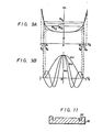
- a yoke 1 made of magnetic material such as ferrite and so on in which a magnetic gap 2 is formed.
- a substrate 3 which incorporates therein an oscillating circuit.
- a coil 6 is wound around at least one of magnetic poles 4 and 5 which are opposed to each other to constitute the magnetic gap 2 of the yoke and a variable current is supplied to the coil 6, thus variable magnetic field applying means being formed.
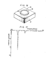
- Fig. 2 is a plan view illustrating an example of the practical construction of the substrate 3 which incorporates therein the oscillating circuit and Fig. 3 is a cross-sectional view taken along a line A-A in Fig. 2.
- a ground conductor 32 is formed on a first major surface of a dielectric substrate 31 made of a material such as alumina and so on.
- a microstrip line 33 is formed on a second major surface of the dielectric substrate 31, one end of which is connected through a conductor 34 to the ground conductor 32.
- the microstrip line 33 is electromagnetically coupled with an YIG thin film magnetic resonance element 35.
- the YIG thin film magnetic resonance element 35 is formed as follows.
- An YIG thin film of ferrimagnetism material is formed on one major surface of, for example, a GGG (gadolinium gallium garnet) substrate 36 by a thin film forming technique such as sputtering, chemical vapor deposition method (CVD method), liquid phase epitaxial growth method (LPE method) and so on and this YIG thin film is shaped as, for example, a disk shaped pattern by photolithography technique.
- reference numeral 37 designates a high frequency bipolar transistor
- reference numeral 38 designates an impedance matching circuit
- reference numeral 39 designates a DC blocking MOS (metal oxide semiconductor) capacitor thereof.
- the base B of the bipolar transistor 37 is connected to a ground pad 40 connected to the ground conductor 32 through a wire 41 which forms a reactance.
- the emitter E thereof is connected to the side of the YIG thin film magnetic resonance element 35 and the collector C thereof is connected to the side of the impedance matching circuit 38, thus a so-called common base series feedback oscillator being formed.
- FIGs. 4A and 4B are respectively block diagrams showing this oscillating circuit.
- reference numeral 42 designates an YIG thin film resonance circuit
- reference numeral 43 designates a negative resistance circuit
- reference numeral 44 designates an impedance matching circuit
- reference numeral 45 designates a load.
- reference numeral 46 designates a load impedance which includes the impedance matching circuit.
- respective reflection coefficients T Y and T N seen to the YIG thin film resonance circuit side or, namely, the YIG feedback circuit side and to the active element side, namely, the negative resistance circuit side from a terminal A are respectively expressed by the following equations using their impedances Z Y and Z N seen from the terminal A.
- Z O is the characteristic imgedance (50 ⁇ ) of the circuit.
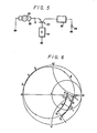
- the negative resistance circuit 43 in Fig. 4 may be a 2-terminal active element serving as a negative resistance element or combination of a circuit made of a 3-terminal active element and feedback element, in the example shown in Figs. 2 and 3, the high frequency bipolar transistor of a 3-terminal active element is used and is formed as the common base series feedback type oscillating circuit as shown in Fig. 5.
- reference letter X designates a reactive circuit.
- 1/T N is in the state on a curve C which is relatively near the inside of the Smith chart, it passes the state shown by a curve D and moves in the direction shown by arrows as the active element operates with a large amplitude.
- the reflection coefficient T Y draws a locus as shown by B in Fig. 6.
- the amplitude condition given by Eq. (7) and the phase condition given by Eq. (5) for starting the oscillation are established at the same time.
- Eqs. (4) and (5) are established at the same time at the frequency f 0 so that the oscillating circuit stationarily oscillates at the oscillation frequency f 0 .
- the resonance frequency of the YIG thin film element 35 is varied in a range from f l to f 2 by varying DC magnetic field applied thereto, the oscillating circuit oscillates in tune with a frequency near the resonance frequency.
- the resonator is formed of the YIG thin film magnetic resonance element which is formed by the thin film forming technique.
- the magnetic resonance element YIG single crystal sphere
- the magnetic resonance element made of a single crystal sphere has an advantage that the magnetostatic mode is difficult to be excited and the sole resonance mode by uniform precession mode can be obtained.
- the magnetic resonance element made of the YIG thin film has, on the other hand, a defect that even if it is located in a good uniform RF magnetic field, magnetostatic mode is excited much because the internal DC magnetic field is not uniform.
- Fig. 8 shows the state of an internal DC magnetic field Hi when a DC magnetic field is applied to the Y I G disk-shaped thin film with a thickness t and a diameter D (radius R) in the direction perpendicular to its surface.
- its aspect ratio t/D is sufficiently small and a magnetic field distribution in the thickness direction of the sample is neglected. Since the demagnetizing field is large in the inside of the disk and becomes suddenly smaller in its outer periphery so that the internal DC magnetic field is small near the center thereof and becomes suddenly large near the outer periphery thereof.
- the magnetostatic mode lies in the region of 0 ⁇ r/R ⁇ ⁇ where w is the resonance angular frequency at the magnetostatic mode and y is the gyromagnetic ratio.
- the resonance frequency is increased as the mode number N becomes large so that the region of the magnetostatic mode is extended gradually to the outside as shown in Fig. 9A.
- annular groove 53 is formed by, for example, a selective etching technique on an YIG thin film magnetic resonance element 52 of, for example, a disc shape which is formed on a GGG substrate 51 to thereby provide an annular thin portion.
- the YIG thin film magnetic resonance element 52 is made sufficiently small in thickness and the magnetostatic mode in this case is (1, N) 1 mode.
- the groove 53 is formed concentrical with the element 52 at a position where the RF magnetization of the (1, 1) 1 mode becomes zero. Further, the groove 53 may be formed continuous or discontinuous. Furthermore, the area encircled by the groove 53 may be formed thin as compared with its outside portion as shown in Fig. 11. In this case, in the inside area close to the groove 53, the demagnetizing field is raised and hence the demagnetizing field becomes substantially uniform up to this area. In other words, as shown by a one-dot chain line in Fig. 9A, the internal DC magnetic field becomes substantially uniform over the wide range in the radius direction. Thus, it becomes possible to suppress much more the excitation of the magnetostatic mode except the uniform mode.
- the magnetization is pinned by the groove 53.
- the groove 53 since the groove 53 is placed at the position where the RF magnetizatior becomes zero for (1, 1) 1 mode, the excitation of (1, 1) 1 mode is not affected.
- the groove 53 is placed at the position where the RF magnetization is not zero originally for other magnetostatic modes so that the magnetization is pinned partially. As a result, the excitation of these modes is weakened so that it is possible to suppress the spurious response without destroying the uniform mode.
- the groove 53 having a radius of 0.8 mm and a depth of 2 ⁇ m was formed on the YIG thin film element having a thickness of 20 ⁇ m and a radius of 1 mm made from the YIG thin film and the ferromagnetic resonance thereof was measured by using the microstrip line. Measured results of its insertion loss were indicated on Fig. 12 and the value of unloaded Q-factor was 775.
- a ferromagnetic resonance was measured by using the microstrip line. Measured results of its insertion loss at that time became as shown in Fig. 13 and the value of the unloaded Q-factor was 660.
- the excitation of the magnetostatic mode except the (1, 1) 1 mode can be suppressed and the spurious response can be suppressed. Further, since the .uniform mode is not damaged, the unloaded Q-factor is never damaged.
- Fig. 14 shows calculated results of the demagnetizing field Hd of an YIG disc having a thickness of 20 ⁇ m and a radius of 1 mm. Since the demagnetizing field Hd is large in the inside of the disc and becomes suddenly small in the peripheral portion thereof, the internal DC magnetic field is small near the center and becomes suddenly large near the outer peripheral portion thereof.
- Fig. 15, shows calculated results of demagnetizing field distribution in a case where the film thickness of the area within the inside of the same YIG thin film with a radius of 0.8 mm is thinned by 1 ⁇ m. From Fig. 15, it will be seen that when the thickness of the inside area is thinned a little, the demagnetizing field near the. peripheral portion of the area with the thickness being reduced is raisea a little and the flat region of the demagnetizing field is widened.
- a ferrimagnetic YIG thin film element 52 is formed on a GGG substrate 51.
- a concave portion 54 is formed on the upper snrface of the YIG thin film element 52 so as to reduce the thickness of the inside area as compared with that of the outside area thereof.
- the thickness of the YIG thin film 52 is made small enough to make the magnetic field distribution in the thickness direction thereof uniform.
- the magnetostatic mode is (1, N) 1 mode.
- the concave portion 54 is extended to a position where the excitation of the magnetostatic mode that becomes the spurious response can be suppressed sufficiently, preferably at a position where the amplitude of the (1, 1) 1 mode becomes zero. For instance, when the YIG thin film element 52 is circular in shape, the concave portion 54 is extended to the position 0.75 to 0.85 times the diameter thereof.
- the disk-shaped concave portion 54 having a depth of 1.7 ⁇ m and a radius of 0.75 mm was concentrically formed on the YIG thin film magnetic resonance element having a thickness of 20 ⁇ m and a radius of 1 mm and the ferromagnetic resonance thereof was measured by using the microstrip line.
- Fig. 17 shows the measured result of the insertion loss thereof. In this case, the value of unloaded Q-factor was 865.
- the resonance frequency of the magnetic resonance element for example, the YIG thin film element depends on the saturation magnetization of the element, the resonance frequency is directly affected by the temperature characteristic of the saturated magnetization. If, in the above-mentioned resonator circuit, the resonance frequency of the YIG thin film element used therein is fluctuated by the change of, for example, the ambient temperature thereof, the resonance frequency will become out of order.
- At least one of the magnetic poles 4 and 5 of the yoke 1 is provided with a soft magnetic plate made of a material having the same temperature characteristic as the YI G thin film element 52, for example, YIG whereby the soft magnetic plate is functioned such that the temperature dependency of the magnetic field in the magnetic gap 2 compensates for the temperature dependency of the YI G thin film element itself, thus the change of the characteristic of the YIG thin film element by the temperature being reduced.
- the magnetic flux generated between the magnetic poles 4 and 5 can be varied by varying the value of the current applied to the coil 6 whereby to vary the oscillation frequency.
- the tuned oscillator using the YIG thin film of this embodiment when the DC magnetic field is varied, (1, N) 1 modes are all equally varied in frequency, no modes are intersected, causing no such defect.
- the both surfaces thereof are not mirror-polished, the unloaded Q-factor can not be raised.
- the YIG thin film produced by the thin film forming technique requires no mirror-polishing and the GGG substrate can be used as the substrate of the tuned oscillator as it is.
- the YIG thin film is used, it is free of the above-described disadvantage which is inherent in the YIG sphere.
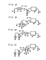
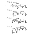
- Figs. 18 to 25 respectively illustrate other embodiments of the tuned oscillator circuit according to this invention.
- Figs. 18 to 25 like parts corresponding to those of Fig. 5 are marked with the same references and will not be described in detail.
- Figs. 18 to 22 illustrate the embodiments of the tuned oscillator circuits which use the bipolar transistor 37 as the active element thereof.
- Figs. 23 to 25, on the other hand, illustrate the embodiments of the tuned oscillator circuits which use a 2-terminal element such as a Gunn diode, an IMPATT diode and the like as the active element thereof.
- Fig. 18 illustrates a modified example of Fig. 5 in which the strip line 33 for coupling is grounded through a characteristic impedance Z 0 .
- ry 0, namely, ry becomes the center of the Smith chart so that the amplitude condition for starting the oscillation is not established, thus a possibility of parasitic oscillation being very small.
- Fig. 19 illustrates the example of the tuned oscillator circuit in which the YIG thin film magnetic resonance element 35 is sandwiched between two coupling strip lines 33 and 33a, the emitter of the transistor 37 is grounded through the strip line 33 and the base of the transistor 37 is grounded through the strip line 33a.
- the YIG thin film magnetic resonance element 35 is located as a band-pass filter in the feedback circuit which serves other than the output circuit, in which when the YIG thin film magnetic resonance element 35 resonates, the positive feedback is applied and the condition of
- the strip lines that are connected to the base and emitter is terminated by the characteristic impedance Z 0 , the possibility of the parasitic oscillation becomes small.
- Fig. 20 illustrates the example of the tuned oscillator circuit in which the emitter of the transistor 37 is grounded through a reactive circuit X 1 , the base of the transistor 37 is grounded through a reactive circuit X 3 and the collector of the transistor 37 is grounded through a series circuit of the coupling strip line 33 of the YIG thin film magnetic resonance element 35, the impedance matching circuit 38 and a load 45.
- the YIG thin film magnetic resonance element 35 is located in the output terminal as a band-blocking filter. A part of the signal is fed back to the negative resistance circuit at the YIG resonance frequency so that this tuned oscillator circuit is operated as the self-injection locking-type oscillator.
- Fig. 21 illustrates the example of the tuned oscillator circuit in which the YIG thin film magnetic resonance element 35 is sandwiched between the coupling strip lines 33 and 33a, the collector of the transistor 37 is grounded through the strip line 33a and the input terminal of the impedance matching circuit 38 is grounded through the strip line 33.
- the YIG thin film magnetic resonance element 35 is located as a band-pass filter in the output terminal and if this YIG thin film magnetic resonance element 35 does not resonate, the load 45 is short-circuited and the phase condition for oscillation is not established. If, on the other hand, the YIG thin film magnetic resonance element 35 resonates, the load 45 and the impedance matching circuit 38 are seen through this YIG thin film magnetic element 35 so that the oscillation condition can be satisfied.
- Fig. 22 illustrates the example of the tuned oscillator circuit in which the tuned oscillator circuit of Fig. 5 is formed as a parallel feedback oscillator.
- the examples of the tuned oscillator circuit of Figs. 20 and 21 can be formed as the parallel feedback oscillator circuit, respectively.
- Fig. 23 illustrates the example of the tuned oscillator circuit in which one terminal of the coupling strip line 33 of the YIG thin film magnetic resonance element 35 is grounded through a 2-terminal active element 37a and the other end of the strip line 33 is grounded through the series circuit of the impedance matching circuit 38 and the load 45, establishing the above-mentioned oscillation condition with respect to the r N and ry seen from the terminal A.
- the YIG thin film magnetic resonance element 35 is located as a band-blocking filter in the output terminal and a part of the signal is fed back to the 2-terminal active element 37a at the YIG resonance frequency so that the tuned oscillator circuit of this embodiment is operated as the self-injection locking-type oscillator.
- Fig. 24 illustrates the example of the tuned oscillator circuit in which one end of the coupling strip line 33 of the YIG thin film magnetic resonance element 35 is grounded, while the other end of this strip line 33 is grounded through the 2-terminal active element 37a and also grounded through the series circuit of the impedance matching circuit 38 and the load 45.
- the negative resistance circuit 43 of Fig. 4 is the 2-terminal active element 37a.
- Fig. 25 illustrates the example of the tuned oscillator circuit in which the YIG thin film magnetic resonance element 35 is sandwiched between the two coupling, strip lines 33 and 33a, one end of the 2-terminal active element 37a is grounded, the other end thereof is grounded through this strip line 33a and the input terminal of the impedance matching circuit 38 is grounded through the strip line 33, other portions being formed similarly to Fig. 23.
- the YIG thin film magnetic resonance element 35 is located as a band-pass filter at the output terminal and if the YIG thin film magnetic resonance element 35 does not resonate, the load 45 is short-circuited and thence the phase condition for oscillation is not established. If, on the other hand, the YIG thin film magnetic resonance element 35 resonates, the load 45 and the impedance matching circuit 38 are seen through the YIG thin film magnetic resonance element 35 so that the oscillation condition can be established.
- the oscillator circuits used in this invention are not limited to the above-described embodiments but other oscillator circuits can of course be applied to the present invention. While in the afore-described embodiments the bipolar transistor is used as the 3-terminal active element, it is needless to say that a field effect transistor can be used as the 3-terminal active element. Furthermore, it is also needless to say that the present invention is not limited to the above-described embodiments but can take various modifications and variations without departing from the gist of the invention.
- the YIG thin film magnetic resonance element formed by the so-called thin film forming technique such as liquid phase epitaxial growth technique, sputtering, chemical liquid phase growth technique and so on is used as the resonator, the advantages of the YIG can be utilized effectively and the defects of the YIG sphere can be improved.
Landscapes
- Inductance-Capacitance Distribution Constants And Capacitance-Resistance Oscillators (AREA)
- Control Of Motors That Do Not Use Commutators (AREA)
Applications Claiming Priority (2)
| Application Number | Priority Date | Filing Date | Title |
|---|---|---|---|
| JP59114793A JPH0770918B2 (ja) | 1984-06-05 | 1984-06-05 | 同調発振器 |
| JP114793/84 | 1984-06-05 |
Publications (3)
| Publication Number | Publication Date |
|---|---|
| EP0164684A2 true EP0164684A2 (de) | 1985-12-18 |
| EP0164684A3 EP0164684A3 (en) | 1988-04-20 |
| EP0164684B1 EP0164684B1 (de) | 1992-03-18 |
Family
ID=14646825
Family Applications (1)
| Application Number | Title | Priority Date | Filing Date |
|---|---|---|---|
| EP85106912A Expired - Lifetime EP0164684B1 (de) | 1984-06-05 | 1985-06-04 | Abgestimmter Oszillator |
Country Status (6)
| Country | Link |
|---|---|
| US (1) | US4626800A (de) |
| EP (1) | EP0164684B1 (de) |
| JP (1) | JPH0770918B2 (de) |
| KR (1) | KR940000428B1 (de) |
| CA (1) | CA1268827A (de) |
| DE (1) | DE3585639D1 (de) |
Cited By (2)
| Publication number | Priority date | Publication date | Assignee | Title |
|---|---|---|---|---|
| EP0320825A3 (en) * | 1987-12-14 | 1989-08-23 | Sony Corporation | Yig tuned oscillator |
| EP0318306A3 (de) * | 1987-11-27 | 1989-08-23 | Sony Corporation | Abgestimmte Oszillatoren |
Families Citing this family (38)
| Publication number | Priority date | Publication date | Assignee | Title |
|---|---|---|---|---|
| JPH0628332B2 (ja) * | 1984-06-05 | 1994-04-13 | ソニー株式会社 | 受信機 |
| US4751480A (en) * | 1986-11-14 | 1988-06-14 | Hewlett-Packard Company | One port magnetostatic wave resonator |
| JP2523600B2 (ja) * | 1987-03-18 | 1996-08-14 | 株式会社日立製作所 | 静磁波発振回路 |
| JPH0633699Y2 (ja) * | 1987-12-28 | 1994-08-31 | ソニー株式会社 | 同調発振器 |
| JPH0287705A (ja) * | 1988-09-24 | 1990-03-28 | Mitsubishi Electric Corp | 同調形発振器 |
| JP2666910B2 (ja) * | 1989-03-24 | 1997-10-22 | 日立金属株式会社 | 静磁波素子 |
| US4988959A (en) * | 1989-10-31 | 1991-01-29 | Avantek, Inc. | YIG tuned oscillator using composite feedback |
| US5204641A (en) * | 1992-03-11 | 1993-04-20 | Space Systems/Loral, Inc. | Conducting plane resonator stabilized oscillator |
| US6179976B1 (en) * | 1999-12-03 | 2001-01-30 | Com Dev Limited | Surface treatment and method for applying surface treatment to suppress secondary electron emission |
| JP3768789B2 (ja) * | 2000-09-07 | 2006-04-19 | アルプス電気株式会社 | 超音波振動子及びウエット処理用ノズル並びにウエット処理装置 |
| EP1344076A1 (de) * | 2000-10-09 | 2003-09-17 | Regents Of The University Of Minnesota | Verfahren und gerät für die bildgebende und die spektroskopische magnetische resonanz unter verwendung von als mikrostreifenübertragungsleitungen ausgebildeten spulen |
| US6690251B2 (en) | 2001-04-11 | 2004-02-10 | Kyocera Wireless Corporation | Tunable ferro-electric filter |
| US7221243B2 (en) | 2001-04-11 | 2007-05-22 | Kyocera Wireless Corp. | Apparatus and method for combining electrical signals |
| US6937195B2 (en) * | 2001-04-11 | 2005-08-30 | Kyocera Wireless Corp. | Inverted-F ferroelectric antenna |
| US7164329B2 (en) | 2001-04-11 | 2007-01-16 | Kyocera Wireless Corp. | Tunable phase shifer with a control signal generator responsive to DC offset in a mixed signal |
| US7154440B2 (en) | 2001-04-11 | 2006-12-26 | Kyocera Wireless Corp. | Phase array antenna using a constant-gain phase shifter |
| US7746292B2 (en) | 2001-04-11 | 2010-06-29 | Kyocera Wireless Corp. | Reconfigurable radiation desensitivity bracket systems and methods |
| US7394430B2 (en) | 2001-04-11 | 2008-07-01 | Kyocera Wireless Corp. | Wireless device reconfigurable radiation desensitivity bracket systems and methods |
| US7174147B2 (en) | 2001-04-11 | 2007-02-06 | Kyocera Wireless Corp. | Bandpass filter with tunable resonator |
| US7071776B2 (en) | 2001-10-22 | 2006-07-04 | Kyocera Wireless Corp. | Systems and methods for controlling output power in a communication device |
| US7176845B2 (en) | 2002-02-12 | 2007-02-13 | Kyocera Wireless Corp. | System and method for impedance matching an antenna to sub-bands in a communication band |
| US7184727B2 (en) | 2002-02-12 | 2007-02-27 | Kyocera Wireless Corp. | Full-duplex antenna system and method |
| US7180467B2 (en) | 2002-02-12 | 2007-02-20 | Kyocera Wireless Corp. | System and method for dual-band antenna matching |
| US7720443B2 (en) | 2003-06-02 | 2010-05-18 | Kyocera Wireless Corp. | System and method for filtering time division multiple access telephone communications |
| WO2005086817A2 (en) * | 2004-03-08 | 2005-09-22 | New York University | Active radio frequency coil for high field magnetic resonance imaging |
| US7248845B2 (en) | 2004-07-09 | 2007-07-24 | Kyocera Wireless Corp. | Variable-loss transmitter and method of operation |
| US20060080414A1 (en) * | 2004-07-12 | 2006-04-13 | Dedicated Devices, Inc. | System and method for managed installation of a computer network |
| WO2006029649A1 (en) * | 2004-09-15 | 2006-03-23 | Commissariat A L'energie Atomique | Microwave oscillator tuned with a ferromagnetic thin film |
| US7548762B2 (en) | 2005-11-30 | 2009-06-16 | Kyocera Corporation | Method for tuning a GPS antenna matching network |
| US7520325B2 (en) * | 2006-02-27 | 2009-04-21 | Geosierra Llc | Enhanced hydrocarbon recovery by in situ combustion of oil sand formations |
| US7986454B1 (en) | 2006-07-03 | 2011-07-26 | Terahertz Technologies Llc | Tunable terahertz generator using a magnon gain medium with an antenna |
| US7706056B2 (en) | 2006-07-03 | 2010-04-27 | Terahertz Technologies Llc | Modulation of terahertz radiation |
| US8031397B1 (en) | 2006-07-03 | 2011-10-04 | Terahertz Technologies, Llc | Three-level magnon laser at room temperatures |
| US7430074B2 (en) * | 2006-07-03 | 2008-09-30 | Terahertz Technologies, Llc | Generation of Terahertz waves |
| US8427740B1 (en) | 2010-03-10 | 2013-04-23 | Terahertz Technologies Llc | Modulation of terahertz radiation at room temperatures |
| JP6691622B1 (ja) | 2019-04-11 | 2020-04-28 | 株式会社フジクラ | 導波路装置 |
| CN113540717B (zh) * | 2021-09-15 | 2021-12-03 | 成都威频科技有限公司 | 一种可调带通滤波器 |
| CN118646371B (zh) * | 2024-08-09 | 2024-11-15 | 成都威频科技有限公司 | 一种低谐波相噪yig振荡器及振荡实现方法 |
Family Cites Families (11)
| Publication number | Priority date | Publication date | Assignee | Title |
|---|---|---|---|---|
| JPS5132252B1 (de) * | 1970-05-21 | 1976-09-11 | ||
| GB1356260A (en) * | 1970-11-05 | 1974-06-12 | Nat Res Dev | Tunable microwave filters |
| FR2116223B1 (de) * | 1970-11-06 | 1974-06-21 | Lignes Telegraph Telephon | |
| US3879677A (en) * | 1973-07-20 | 1975-04-22 | Varian Associates | Tuned oscillator circuit having a tuned filter output |
| US4152676A (en) * | 1977-01-24 | 1979-05-01 | Massachusetts Institute Of Technology | Electromagnetic signal processor forming localized regions of magnetic wave energy in gyro-magnetic material |
| FR2419609A1 (fr) * | 1978-03-07 | 1979-10-05 | Thomson Csf | Oscillateur du type " tri-porte ", accordable electroniquement sur une tres large bande de frequences |
| FR2447641A1 (fr) * | 1979-01-26 | 1980-08-22 | Thomson Csf | Oscillateur accordable hyperfrequence a ondes magnetostatiques |
| JPS58182302A (ja) * | 1982-04-19 | 1983-10-25 | Sony Corp | 磁性共鳴装置 |
| CA1204181A (en) * | 1982-12-06 | 1986-05-06 | Yoshikazu Murakami | Ferromagnetic resonator |
| US4528529A (en) * | 1983-12-12 | 1985-07-09 | Hewlett-Packard Company | Magnetostatic wave resonator |
| JPH0628332B2 (ja) * | 1984-06-05 | 1994-04-13 | ソニー株式会社 | 受信機 |
-
1984
- 1984-06-05 JP JP59114793A patent/JPH0770918B2/ja not_active Expired - Lifetime
-
1985
- 1985-06-03 US US06/740,813 patent/US4626800A/en not_active Expired - Lifetime
- 1985-06-03 CA CA000483024A patent/CA1268827A/en not_active Expired - Lifetime
- 1985-06-04 DE DE8585106912T patent/DE3585639D1/de not_active Expired - Lifetime
- 1985-06-04 EP EP85106912A patent/EP0164684B1/de not_active Expired - Lifetime
- 1985-06-05 KR KR1019850003927A patent/KR940000428B1/ko not_active Expired - Fee Related
Cited By (2)
| Publication number | Priority date | Publication date | Assignee | Title |
|---|---|---|---|---|
| EP0318306A3 (de) * | 1987-11-27 | 1989-08-23 | Sony Corporation | Abgestimmte Oszillatoren |
| EP0320825A3 (en) * | 1987-12-14 | 1989-08-23 | Sony Corporation | Yig tuned oscillator |
Also Published As
| Publication number | Publication date |
|---|---|
| KR940000428B1 (ko) | 1994-01-20 |
| EP0164684B1 (de) | 1992-03-18 |
| DE3585639D1 (de) | 1992-04-23 |
| JPS60257607A (ja) | 1985-12-19 |
| CA1268827A (en) | 1990-05-08 |
| JPH0770918B2 (ja) | 1995-07-31 |
| US4626800A (en) | 1986-12-02 |
| KR860000746A (ko) | 1986-01-30 |
| EP0164684A3 (en) | 1988-04-20 |
Similar Documents
| Publication | Publication Date | Title |
|---|---|---|
| US4626800A (en) | YIG thin film tuned MIC oscillator | |
| KR940000431B1 (ko) | 신호 변환기 | |
| EP0320825B1 (de) | Oszillator mit YIG-Abstimmung | |
| US4743874A (en) | Magnetostatic wave tunable resonator | |
| US5801591A (en) | Microwave linear oscillator/amplifier utilizing a multicoupled ferrite resonator | |
| US4992760A (en) | Magnetostatic wave device and chip therefor | |
| US3879677A (en) | Tuned oscillator circuit having a tuned filter output | |
| US4939488A (en) | Magnetostatic wave device | |
| US5053734A (en) | Magnetostatic wave device | |
| CN1003971B (zh) | 调谐振荡器 | |
| JPH0213101A (ja) | フェリ磁性薄膜共鳴素子 | |
| JPH061886B2 (ja) | 受信機 | |
| Omori | The YIG-Tuned Gunn Oscillator, Its Potentials and Problems | |
| JPH03262301A (ja) | マイクロ波装置 | |
| JPH06177643A (ja) | 静磁波発振回路 | |
| GB2194685A (en) | Ferromagnetic resonance devices | |
| JPH03182104A (ja) | 同調形発振器 | |
| JPH02170606A (ja) | 同調発振器 | |
| JPH03178207A (ja) | 同調形発振器 | |
| JPS60260202A (ja) | 帯域通過フイルタ | |
| Ollivier | A 3.0-6.5 GHz YIG-tuned transistor oscillator/amplifier | |
| JP2508424C (de) | ||
| JPH0766610A (ja) | 強磁性磁気共鳴装置 | |
| JPH0340501A (ja) | マイクロ波装置 | |
| JPS61108203A (ja) | 電子同調回路 |
Legal Events
| Date | Code | Title | Description |
|---|---|---|---|
| PUAI | Public reference made under article 153(3) epc to a published international application that has entered the european phase |
Free format text: ORIGINAL CODE: 0009012 |
|
| AK | Designated contracting states |
Designated state(s): DE FR GB NL |
|
| PUAL | Search report despatched |
Free format text: ORIGINAL CODE: 0009013 |
|
| AK | Designated contracting states |
Kind code of ref document: A3 Designated state(s): DE FR GB NL |
|
| 17P | Request for examination filed |
Effective date: 19880418 |
|
| 17Q | First examination report despatched |
Effective date: 19900502 |
|
| GRAA | (expected) grant |
Free format text: ORIGINAL CODE: 0009210 |
|
| AK | Designated contracting states |
Kind code of ref document: B1 Designated state(s): DE FR GB NL |
|
| REF | Corresponds to: |
Ref document number: 3585639 Country of ref document: DE Date of ref document: 19920423 |
|
| ET | Fr: translation filed | ||
| PLBE | No opposition filed within time limit |
Free format text: ORIGINAL CODE: 0009261 |
|
| STAA | Information on the status of an ep patent application or granted ep patent |
Free format text: STATUS: NO OPPOSITION FILED WITHIN TIME LIMIT |
|
| 26N | No opposition filed | ||
| PGFP | Annual fee paid to national office [announced via postgrant information from national office to epo] |
Ref country code: DE Payment date: 20010528 Year of fee payment: 17 |
|
| PGFP | Annual fee paid to national office [announced via postgrant information from national office to epo] |
Ref country code: GB Payment date: 20010530 Year of fee payment: 17 |
|
| PGFP | Annual fee paid to national office [announced via postgrant information from national office to epo] |
Ref country code: FR Payment date: 20010611 Year of fee payment: 17 |
|
| PGFP | Annual fee paid to national office [announced via postgrant information from national office to epo] |
Ref country code: NL Payment date: 20010628 Year of fee payment: 17 |
|
| REG | Reference to a national code |
Ref country code: GB Ref legal event code: IF02 |
|
| PG25 | Lapsed in a contracting state [announced via postgrant information from national office to epo] |
Ref country code: GB Free format text: LAPSE BECAUSE OF NON-PAYMENT OF DUE FEES Effective date: 20020604 |
|
| PG25 | Lapsed in a contracting state [announced via postgrant information from national office to epo] |
Ref country code: NL Free format text: LAPSE BECAUSE OF NON-PAYMENT OF DUE FEES Effective date: 20030101 Ref country code: DE Free format text: LAPSE BECAUSE OF NON-PAYMENT OF DUE FEES Effective date: 20030101 |
|
| GBPC | Gb: european patent ceased through non-payment of renewal fee |
Effective date: 20020604 |
|
| PG25 | Lapsed in a contracting state [announced via postgrant information from national office to epo] |
Ref country code: FR Free format text: LAPSE BECAUSE OF NON-PAYMENT OF DUE FEES Effective date: 20030228 |
|
| NLV4 | Nl: lapsed or anulled due to non-payment of the annual fee |
Effective date: 20030101 |
|
| REG | Reference to a national code |
Ref country code: FR Ref legal event code: ST |