EP0167387A2 - Dispositif de traitement d'un signal vidéo - Google Patents
Dispositif de traitement d'un signal vidéo Download PDFInfo
- Publication number
- EP0167387A2 EP0167387A2 EP85304696A EP85304696A EP0167387A2 EP 0167387 A2 EP0167387 A2 EP 0167387A2 EP 85304696 A EP85304696 A EP 85304696A EP 85304696 A EP85304696 A EP 85304696A EP 0167387 A2 EP0167387 A2 EP 0167387A2
- Authority
- EP
- European Patent Office
- Prior art keywords
- input
- signal
- processing apparatus
- video signal
- output
- Prior art date
- Legal status (The legal status is an assumption and is not a legal conclusion. Google has not performed a legal analysis and makes no representation as to the accuracy of the status listed.)
- Granted
Links
Images


Classifications
-
- H—ELECTRICITY
- H04—ELECTRIC COMMUNICATION TECHNIQUE
- H04N—PICTORIAL COMMUNICATION, e.g. TELEVISION
- H04N5/00—Details of television systems
- H04N5/14—Picture signal circuitry for video frequency region
- H04N5/20—Circuitry for controlling amplitude response
-
- H—ELECTRICITY
- H04—ELECTRIC COMMUNICATION TECHNIQUE
- H04N—PICTORIAL COMMUNICATION, e.g. TELEVISION
- H04N5/00—Details of television systems
- H04N5/14—Picture signal circuitry for video frequency region
- H04N5/21—Circuitry for suppressing or minimising disturbance, e.g. moiré or halo
-
- H—ELECTRICITY
- H04—ELECTRIC COMMUNICATION TECHNIQUE
- H04M—TELEPHONIC COMMUNICATION
- H04M5/00—Manual exchanges
- H04M5/18—Arrangements for signalling the class or number of called or calling line from one exchange to another
- H04M5/20—Arrangements for indicating the numbers of the incoming lines
Definitions
- This invention relates to a video signal processing apparatus capable of removing noise effectively without deteriorating the picture quality for use in a video tape recorder (VTR) or the like.
- VTR video tape recorder
- apparatus for removing low level noise of high frequency band signal and noise removing apparatus utilizing the line correlation are used to remove noises mixed in the reproduced signals.
- Fig. l(a) is its block diagram, in which numeral 12 is an input terminal of reproduced and demodulated luminance signal, 13 is a high pass filter, 14 is a limiter, 15 is a subtractor, and 16 is an output terminal of the signal with reduced noise.
- the operation of the noise removing circuit thus composed is as follows.
- the high-pass filter 13 has a frequency characteristic as indicated by solid line in Fig. 1(b), for example, when the horizontal frequency f H is taken on the axis of abscissas, and the noise and signal in high band are led into the limiter 13.
- the limiter 13 is composed usually of semiconductor nonlinear elements, and its input-output characteristic is as shown in Fig. 2. Accordingly, when the input component of the limiter is a noise with a small amplitude, it passes through the limiter and is subtracted by the subtractor 15, and the frequency characteristic of the apparatus from the input terminal 12 to output terminal 14 becomes a low-pass performance as shown by broken line in Fig.
- 3(a) is a schematic structural drawing of the conventional noise removing apparatus utilizing the line correlation, in which numeral 1 is an input terminal of reproduced FM luminance signal, 4 is a glass delay line for delaying the FM signal by 1H, 5 and 6 are demodulators for frequency demodulation, 7 is a subtractor for obtaining the difference between the demodulated luminance signal and the 1H delayed luminance signal, 8 is an attenuator for attenuating the output signal of the subtractor 7 to about 1/2, 9 is a limiter for limiting the amplitude of signal, 10 is an adder for adding the output signal of demodulator 5 and output signal of limiter 9, and 11 is an output terminal of signal.
- An example of such noise removing apparatus is disclosed in the Japanese Unexamined Patent Publication Sho. 55-80966.
- the operation of thus composed noise removing apparatus utilizing the line correlation is as follows.
- the line from the input terminal to limiter 9 has the so-called C-shaped comb line filter characteristic with respect to the demodulated signals, and when the vertical frequency f v is taken on the axis of abscissas, in the case of NTSC system, the frequency characteristic becomes as shown by solid line in Fig. 3(b) (where cy/ph refers to cycles/picture height),.and the noise without line correlation and signal are fed into the limiter 9.
- the input- output characteristic of the limiter 9 is as shown in Fig. 2.
- the apparatus from the input terminal 1 to the output terminal 11 has the so-called Y-shaped comb line filter characteristic with respect to the demodulated signal, so that the noise in the vicinity of the vertical frequency 525/4 (cy/ph) as indicated by broken line in Fig. 3(b) is removed.
- the component fed into the limiter 9 is a signal without line correlation having a large amplitude, since the amplitude is limited by the limiter, the output signal from the demodulator 5 is delivered almost directly to the output terminal 11, without being removed. Thus the vertical resolution of the picture is not deteriorated so much.
- the noise removing apparatus utilizing the line correlation, since the 1H delay is effected in the form of FM signal by using glass delay line, two demodulators are required, and yet the noise removing effect may not be exhibited sufficiently due to the instability of frequency characteristic of the glass delay line or inaccuracy of delay time. It was also difficult to reduce the size of the apparatus.
- This invention is intended to solve the above-discussed problems in the prior art, and is further intended to present a video signal processing apparatus capable of obtaining an excellent noise removing effect without deteriorating the signal, while simplifying the structure of the apparatus and reducing the manufacturing cost.
- a video signal processing apparatus of this invention comprises a digital filter for passing a specific frequency band of digitized input luminance signal, and a nonlinear processing circuit for nonlinearly processing the output of the digital filter, wherein the pass band component of the filter is suppressed or emphasized depending on the input signal amplitude of the nonlinear processing circuit.
- the apparatus comprises a high-pass filter for passing the high band component of digitized input luminance signal, a nonlinear processing circuit for non- linearly processing the output of the high-pass filter, and an arithmetic circuit for mixing the input luminance signal with the output signal of the nonlinear processing circuit.
- the input-output characteristic of the nonlinear processing circuit can be freely set. Therefore, by determining this characteristic in a way to suppress the frequency component passing through the filter, of the input luminance signal, in a small amplitude range of input signal of the nonlinear processing circuit, the noise can be reduced without deteriorating the signal quality. Furthermore, in a range where the input signal amplitude of the nonlinear processing circuit is larger than a specified level, by determining the nonlinear input-output characteristic in such a way as to emphasize the frequency component passing through the filter, the picture can be clarified without emphasizing the noise.
- any nonlinear input-output characteristic can be easily realized, for example, by using ROM.
- the nonlinear processing circuit so as to select any desired one of plural kinds of input-output characteristics, the noise reduction extent and the picture resolution can be freely adjusted depending on the nature of the picture, S/N ratio or the taste of the user.
- the filter when the filter is designed in a band-pass type one, the noise in the medium range which is likely to impede visually may be removed.
- the filter is a one which relates the vertical frequency by using the memory for delaying the signal by one horizontal scanning period
- many defects of the glass delay line may be overcome as compared with the conventional noise removing apparatus utilizing the line correlation by glass delay line, and an excellent noise removing effect can be obtained, and the demodulator is required only in one line.
- the apparatus may be comprised by plural filter means for dividing the horizontal and vertical two-dimensional frequency regions of digitized input luminance signals into plural two-dimensional frequency regions, nonlinear processing means for nonlinearly processing the outputs of the plural filters, and a mixing means for mixing the outputs of the nonlinear processing means.
- the signals are individually processed nonlinearly and synthesized.
- the noise and signal can be separated smoothly in each nonlinear processing circuit, and only the noise can be suppressed without deteriorating the delicate luminance changes.
- noise when noise is superposed on the signal, by separately processing nonlinearly the frequency band including the signal spectrum and the other frequency band, a beautiful picture can be obtained by effectively removing the overlaying noise.
- optimum nonlinear characteristics may be determined depending on the signal of the individual divided frequency bands, noise property, and visual characteristics, and an excellent noise removing effect can be obtained by keeping the deterioration of visual picture quality to a minimum.
- the dropout may be compensated. Since this dropout compensation function is to drop out in the form of digital signal after demodulating the reproduced FM signal, the noise occurring due to discontinuation at the changing point of the phase of FM signal as experienced conventional does not take place. Or a dropout extending over a long period exceeding lH may be smoothly compensated because the data is delayed in the form of digital signal, without deterioration of the picture quality due to decrease of amplitude or band as experienced conventionally.
- Fig. 4 is a circuit block diagram of a video signal processing apparatus in a first embodiment of this invention, in which numeral 117 is an input terminal of luminance signal which has been digitized after being reproduced from the VTR and frequency demodulated, and 118 is a filter.
- This filter 118 is composed of a delay circuit 119 with delay time D, an arithmetic circuit 120, and a coefficient circuit 121.
- Numeral 122 is a nonlinear processing circuit for nonlinearly processing the output signal from the filter 118
- 123 is an adder for adding the output signal of the nonlinear processing circuit 122 and the input luminance signal
- 124 is an output terminal for delivering the processed signal.
- the frequency characteristic of the filter 118 is a high band passing type performance as shown in Fig. 5 when, for example, the delay time D is about 14 nsec, and the higher band portion of the luminance signal fed into the input terminal 117 is allowed to pass and supplied into the nonlinear processing circuit 122.
- Supposing the input-output characteristic of the nonlinear processing circuit 122 to be as indicated by solid line C in Fig. 6(a) the signal fed to the input terminal 117 appears directly at the output terminal 124 in Fig. 4, and the frequency characteristic of the line from the input terminal 117 to the output terminal 124 becomes as shown by solid line Q in Fig. 6(b).
- the high band component is extracted by the filter 118, and fed into the nonlinear processing circuit 122.
- the luminance signal is mostly composed of low frequency components
- the extracted high band components with a small amplitude may be almost regarded as the noise.
- the frequency characteristic of the apparatus becomes as shown by solid line 0 in Fig. 6 if the high band component obtained by the filter 118 in Fig. 4 is low in level and may be regarded as noise, so that the noise in the high band may be suppressed.
- the frequency characteristic of the device becomes as shown by solid line Q in Fig. 6(b), so that the signal may not be deteriorated.
- the nonlinear characteristic in Fig. 7(a) since the output does not become 0 if the input is sufficiently large, the resolution may be deteriorated more or less. Accordingly, it is possible to modify the nonlinear characteristic as shown in Fig. 7(b). As a result, the resolution of the signal will never be deteriorated.
- this characteristic since it is discontinuous in the threshold area, an unnatural impedance may be caused in this discontinuous part depending on the threshold level. In this case, as shown in Fig.
- the resolution of the picture can be enhanced.
- the resolution of the picture can be further enhanced even in a signal with a relatively small amplitude.
- the noise is suppressed by the frequency characteristic of solid line 0 in Fig. 6(b), while the signal is emphasized in the high band by the-characteristic of solid line S in Fig. 6(b).
- various compositions may be considered by proper combination of logic circuits depending on the individual characteristics, and by using read-only memories (hereinafter referred to ROM), various nonlinear characteristics may be realized very easily. That is, using the input signal to the nonlinear processing circuit 122 as the address, a desired characteristic can be realized by composing so that the memory content corresponding to the address is delivered as output signal, and by storing the predetermined input-output characteristics.
- ROM read-only memories
- the input-output characteristic of the nonlinear processing circuit can be freely set, and it can be easily realized, in particular, by using ROM.
- the characteristic to suppress the noise without deteriorating the signal the characteristic to improve the resolution of the picture without emphasizing the noise, and even the characteristic to suppress the noise and improve the picture resolution at the same time can be easily realized.
- all processings are effected in the form of digital signal, all components can be formed on one-chip semiconductor, so that reduction of size and manufacturing cost of the apparatus can be realized. Thus, many advantages are brought about.
- the nonlinear processing circuit 122 has one nonlinear input-output characteristic, but it may be also possible to possess plural nonlinear input-output characteristics and use one of them selectively.
- numeral 129 is a nonlinear processing circuit
- 127 and 12E are input and output terminals of the nonlinear processing circuit 129.
- This nonlinear processing circuit 129 comprises nonlinear input/output circuits 130a to 130n possessing different nonlinear input-output characteristics, and a switch 131 to select one of these nonlinear input/output circuits 130a to 130n, and this switch 131 is controlled by a control signal 132.
- This nonlinear processing circuit 129 can be easily realized, for example, by storing plural kinds of input-output characteristics in a table in a ROM and selecting one of them. By using such ncnlinear processing circuit 129, the frequency correction and noise reduction range can be properly adjusted depending on the property of picture, S/N ratio or the taste of the user.
- Fig. 9 is a circuit block diagram of a video signal processing apparatus in a second embodiment of this invention, in which numeral 133 is a filter composed of delay circuits 134a and 134b each with delay time D, coefficient circuits 135a to 135c with coefficeints 1/4, -1/2 and 1/4 respectively, and an adder 136, and numeral 137 is a delay circuit with delay time D for feeding the input luminance signal into the adder 132.
- the delaytime from the input of the filter 118 to its output varies with the frequency, and the delay time of the signal from the input terminal 117 to the output terminal 124 varies, as a result of the above, depending on the frequency of input signal or characteristic of the non- linear processing circuit 122, so that the picture quality may be unnaturally deteriorated.
- the delay time between input and output of the filter 133 remains constant (D) regardless of the frequency of signal, and the delay time of the signal from input terminal 117 to output terminal 124 is always D, as a result of insertion of the delay circuit 137, regardless of the frequency or nonlinear processing characteristic, so that the signal may not be deteriorated.
- the delay circuit 137 may be commonly replaced by the delay circuit 134a, so that the circuit scale can be reduced.
- Fi g . 10 is a circuit block diagram of a video signal processing apparatus in a third embodiment of this invention, which differs from the second embodiment shown in Fig. 9 only in the filter composition and its frequency characteristic.
- Numeral 138 is a filter, which is composed of delay circuits 139a to 139c with delay time 3D, 2D and D, respectively, operating circuits 140a to 140c, and a coefficient circuit 141 with coefficient of 1/8.
- the delay circuit 139a also functions to delay the signal being led into the adder 132, without passing through the filter 138, by delay time 3D.
- the frequency characteristic of this filter 139 becomes a band passing type as shown in Fig. 11 when, for example, the delay time D is about 140 nsec.
- the noise region or signal in a medium band of around 1 to 2 MHz can be emphasized.
- the noise in the medium band which is more impeding than the high band noise visually can be lessened.
- a filter relating to the vertical frequency is used.
- Fig. 13 is a circuit block diagram of a video signal processing apparatus in the fourth embodiment of this invention, in which numeral 210 is an input terminal being fed with a luminance signal after being reproduced by the VTR, frequency-modulated, demodulated and digitized, 211 is a digital memory for delaying the input luminance signal by one horizontal scanning period (1H), 212 is a subtractor for subtracting the signal delayed by the digital memory 211 from the input luminance signal, 213 is a coefficient circuit for multiplying the output signal of the subtractor 212 by 1/2, 214 is a nonlinear processing circuit for delivering a specific output depending on the amplitude of the output signal of the coefficient circuit 213, 215 is a subtractor for subtracting the output of the nonlinear processing circuit 214 from the input signal, and 216 is an output terminal where a noise reduced output is obtained.
- the nonlinear processing circuit 214 is, similarly to the embodiment shown in Fig. 4, composed of, for example, a ROM.
- the operation of the video signal processing apparatus in this embodiment thus composed is basically same as that of the prior art shown in Fig. 3, and the frequency characteristic from the input terminal 210 to the input of the nonlinear processing circuit 214 is as indicated by solid line in Fig. 3(b) in the case of NTSC system, and the frequency characteristic of the circuit from the input terminal 210 to the output terminal 216 varies with the amplitude of the input signal of the nonlinear processing circuit 214.
- the input-output characteristic of the nonlinear processing circuit 214 can be freely realized as shown in Fig. 7 same as in the case of the preceding embodiment shown in Fig. 4, so that the reduction of noise and enhancement of resolution can be achieved.
- the size can be reduced; the cost is lowered by the semiconductor composition, as compared with the conventional use of glass delay line; only one demodulator is used; and sufficient noise removing effect can be exhibited.
- any desired non- linear input-output characteristic can be realized. As a result, it is possible to remove only noise without deteriorating the vertical resolution as compared with the prior art, and the characteristic to suppress the noise and improve the vertical resolution of the signal at the same time can be also realized.
- the nonlinear processing circuit 214 it is possible to compose the nonlinear processing circuit 214 to possess plural input- output characteristics as shown in Fig. 8. As a result, by selecting the input-output characteristic properly depending on the type of picture or level of noise, it is possible to adjust the amount of noise reduction and the emphasis of the vertical resolution.
- the embodiments comprising plural digital filter means for dividing the horizontal and vertical two-dimensional frequency region of digitized input luminance signal into plural two-dimensional frequency bands, plural nonlinear processing means for nonlinearly processing the outputs of the plural filters, and a mixing means to mix the outputs of the plural nonlinear processing means.
- the signal component and noise component may be separated more clearly, and the noise can be suppressed without deteriorating the signal component, and also the noise component superposing on the signal can be reduced efficiently.
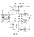
- Fig. 14 is a configuration of video signal processing apparatus in a fifth embodiment of this invention, in which numeral 317 is an input signal of reproduced FM luminance signal being demodulated and digitized, and 322 is an output signal of the signal lowered in the noise level.
- Numeral 325 is a memory for delaying the signal by 1H
- 326 is an adder
- 327 is a subtractor
- 332 and 333 are adders
- 334 and 335 are coefficient circuits for doubling the signal
- 336 and 338 are adders
- 337 and 339 are subtractors
- 340 and 341 are coefficient circuits for multiplying the signal by 1/8
- 344 to 346 are nonlinear processing circuits having nonlinear input-output characteristics
- 347 is an adder for mixing the four output signals of the nonlinear processing circuits 344 to 346 and coefficient circuit 341.
- the transfer functions from the input terminal 317 to the coefficient circuits 340 to 343 are defined as follows, supposing the delay of delay time D to be z -1 and the delay of H to be w -1
- these transfer functions may be as shown in Figs. 15(a) to (d), respectively, in the case of NTSC system when D is about - 140 nsec.
- these frequency characteristics are expressed as shown in Figs. 15(e) to (h) (where, however, the signal band is limited to f H ⁇ 3 MHz, f v ⁇ 525/2 cy/ph).
- the shaded areas refer to the frequency region with the gain of frequency characteristics in (a) to (d) of about -3 dB or more.
- the four outputs from the input terminal 317 to the coefficient circuits 340 to 343 in the configuration of Fig. 14 are respectively filters to divide the two-dimensional frequency region into four bands.
- the characteristic of the apparatus from the input terminal 317 to the output of adder 34-7 is such that the outputs of four filters are synthesized in the adder 347, if the signal passes through nonlinear processing circuit 344 to 346 without undergoing change, and the transfer coefficient will be the sum of equations (1) to (4), that is,
- the signal from the input terminal 317 is delayed by D, and it does not affect the frequency characteristic of the signal.
- the transfer function of the apparatus from the input end of 320 tc the output of adder 347 is the sum of only equations (1) to (3).
- the frequency characteristic at this time is, referring to Fig. 16, such that only the two-dimensional frequency band of IV is attenuated to -3 dB or less.
- the nonlinear processing circuits 344, 345 do not allot to pass signal, the frequency bands of II, III in Fig. 16 are attenuated, respectively.
- the frequency band of the output of the filter 133 corresponds, in Fig. 16, to bands II and IV.
- the band of the signal fed into the nonlinear processing circuit 214 corresponds to bands III and IV in Fig. 16. In both cases, the band is about 1/2 of the total two-dimensional frequency region, and it must be noted that a relatively large energy is led into the nonlinear processing circuit.
- the operation of cascade connection of the embodiments of Fig. 13 and Fig. 9 is as follows.
- the noise contained in the signal reproduced by the VTR is a white noise over an entire band, while the signal spectrum is concentrated in a narrow frequency band. Supposing the signal spectrum is present only in region I in Fig. 16, since the regions III and IV led into the nonlinear processing circuit in Fig. 13 and the regions II and IV led into the nonlinear processing circuit in Fig. 9 are both noise components of a small amplitude only, and noise existing in the frequency regions of II to IV will be suppressed. Or, if a signal spectrum with large amplitude is concentrated in the region III, the noise reducing effect by the apparatus in Fig.
- the signals led into individual nonlinear processing circuits are about 1/4 of the total two-dimensional frequency region of the signal, being narrower as compared with the frequency band led into the nonlinear processing circuit in the embodiment shown in Fig. 9 or Fig. 8. Therefore, of the noise uniformly distributing in the entire band, the amplitude of the noise led into the respective nonlinear processing circuits decreases, and the non-passing amplitude of the nonlinear input-output characteristic shown in Fig. 17(a) can be set smaller. To the contrary, since the signal components are concentrated in a narrow frequency band, one of the four filter outputs is concentrated, and the amplitude does not decrease so much. As a result, the signal and noise can be separated clearly, and only the noise can be reduced without much deteriorating delicate luminance changes. That is a first feature of this embodiment.
- a third feature is that different nonlinear processings can be given to the three frequency regions II to IV in Fi g . 16.
- the reproduced signal of VTR is deteriorated in the high band of horizontal frequency.
- the noise component in high band is hardly impeding visually, as compared with the noise in medium or low band.
- the nonpassing amplitude of the nonlinear processing circuit in the regions II and IV smaller as compared with the region III containing the signal in the medium or low band of the horizontal frequency, deterioration of small signals in high band can be prevented, so that the picture can be visually improved.
- Concerning the frequency regions of II and IV while the region II comprises signals of fine vertical patterns, the region IV corresponds to signals of fine oblique patterns.
- the oblique pattern is not so important for small signals, as compared with the vertical pattern, with respect to the picture quality and visual effect. Accordingly, as compared with the non-passing amplitude of the nonlinear processing circuit with respect to region II, by setting that of the region IV somewhat larger, the larger noise can be suppressed while hardly deteriorating the picture quality visually.
- the optimum nonlinear characteristic can be determined separately depending on the signal of divided frequency regions and nature of noise.
- this embodiment owns numerous excellent features.
- the entire device may be composed of semiconductors and structured as one-chip IC, so that the device can be small-sized, adjustment- free, and lowered in cost, while only one frequency demodulator is needed.
- the nonlinear processing circuits 344, 345 and 346 may be composed to realize plural nonlinear input-output characteristics as shown in Fig. 8.
- Fig. 18 is a configuration of a video processing apparatus in the seventh embodiment of this invention. What differs from the sixth embodiment shown above lies in the dropout compensating function making use of the signal delayed by lH which is obtained at the time of making up the two-dimensional filter.
- numeral 323 is an input terminal of dropout detection signal to tell the presence or absence of dropout
- 324 is a switch to be controlled by the dropout detection signal, and other parts are same as in the embodiment shown in Fi g . 14 and are given the same numerals.
- the operation of thus composed embodiment is as follows.
- the switch 323 is usually connected to the upper side, where an excellent noise removing effect is obtained exactly the same as in the embodiment shown in Fig. 14.
- the switch 324 is connected to the lower side by the dropout detection signal fed from the switch 323.
- the output of the switch 324 is replaced by the 1H delayed signal, so that the dropout is compensated.
Landscapes
- Engineering & Computer Science (AREA)
- Signal Processing (AREA)
- Multimedia (AREA)
- Picture Signal Circuits (AREA)
- Television Signal Processing For Recording (AREA)
Applications Claiming Priority (8)
| Application Number | Priority Date | Filing Date | Title |
|---|---|---|---|
| JP59135753A JPH0681269B2 (ja) | 1984-06-30 | 1984-06-30 | 映像信号処理装置 |
| JP59135752A JPS6116068A (ja) | 1984-06-30 | 1984-06-30 | 映像信号処理装置 |
| JP135753/84 | 1984-06-30 | ||
| JP135752/84 | 1984-06-30 | ||
| JP59175928A JPS6153883A (ja) | 1984-08-24 | 1984-08-24 | 映像信号処理装置 |
| JP175928/84 | 1984-08-24 | ||
| JP59185850A JPS6163169A (ja) | 1984-09-05 | 1984-09-05 | 映像信号処理装置 |
| JP185850/84 | 1984-09-05 |
Publications (3)
| Publication Number | Publication Date |
|---|---|
| EP0167387A2 true EP0167387A2 (fr) | 1986-01-08 |
| EP0167387A3 EP0167387A3 (en) | 1988-07-27 |
| EP0167387B1 EP0167387B1 (fr) | 1993-02-03 |
Family
ID=27471949
Family Applications (1)
| Application Number | Title | Priority Date | Filing Date |
|---|---|---|---|
| EP85304696A Expired - Lifetime EP0167387B1 (fr) | 1984-06-30 | 1985-07-01 | Dispositif de traitement d'un signal vidéo |
Country Status (4)
| Country | Link |
|---|---|
| US (1) | US4827342A (fr) |
| EP (1) | EP0167387B1 (fr) |
| KR (1) | KR890004220B1 (fr) |
| DE (1) | DE3587053T2 (fr) |
Cited By (6)
| Publication number | Priority date | Publication date | Assignee | Title |
|---|---|---|---|---|
| US4760449A (en) * | 1985-04-03 | 1988-07-26 | Matsushita Electric Industrial Co., Ltd. | Video signal processing apparatus |
| EP0267786A3 (en) * | 1986-11-11 | 1990-04-04 | Matsushita Electric Industrial Co., Ltd. | Noise reduction apparatus for video signal |
| EP0331017A3 (en) * | 1988-02-29 | 1990-06-13 | Kabushiki Kaisha Toshiba | Picture quality adjusting circuit with fir filter for digital processing |
| GB2234133A (en) * | 1989-07-14 | 1991-01-23 | Mitsubishi Electric Corp | Video noise reduction apparatus |
| GB2250886A (en) * | 1990-12-13 | 1992-06-17 | Rank Cintel Ltd | Noise reduction in video signals |
| US5974193A (en) * | 1996-01-08 | 1999-10-26 | Nds Limited | Relating to noise reduction |
Families Citing this family (17)
| Publication number | Priority date | Publication date | Assignee | Title |
|---|---|---|---|---|
| US5534948A (en) * | 1989-08-15 | 1996-07-09 | Rank Cintel Limited | Method and apparatus for reducing the effect of alias components produced through non-linear digital signal processing, such as gamma correction, by selective attenuation |
| JPH03112275A (ja) * | 1989-09-27 | 1991-05-13 | Sony Corp | 雑音低減回路 |
| US5260775A (en) * | 1990-03-30 | 1993-11-09 | Farouda Yves C | Time domain television noise reduction system |
| EP0449656A3 (en) * | 1990-03-30 | 1992-03-18 | Yves Charles Faroudja | Time domain television noise reduction system |
| JPH0468923A (ja) * | 1990-07-09 | 1992-03-04 | Sony Corp | ノンリニアプリエンファシス・デエンファシスシステム |
| US5119195A (en) * | 1991-01-31 | 1992-06-02 | Thomson Consumer Electronics, Inc. | Video noise reduction system employing plural frequency bands |
| JP2783696B2 (ja) * | 1991-05-31 | 1998-08-06 | シャープ株式会社 | 画質補正装置 |
| US5392070A (en) * | 1991-11-26 | 1995-02-21 | Kabushiki Kaisha Toshiba | Apparatus for correcting faulty pixel signals by replacing the faulty pixel signals with normal pixel signals |
| US5384865A (en) * | 1992-06-01 | 1995-01-24 | Eastman Kodak Company | Adaptive, hybrid median filter for temporal noise suppression |
| JPH09215007A (ja) * | 1996-02-01 | 1997-08-15 | Sony Corp | 映像信号処理回路 |
| US6493039B1 (en) * | 1999-01-19 | 2002-12-10 | Xerox Corporation | Method and apparatus for white noise reduction in video images |
| JP2007172170A (ja) * | 2005-12-20 | 2007-07-05 | Fujitsu Ltd | 画像処理回路及び画像処理方法 |
| US8134646B2 (en) * | 2006-05-24 | 2012-03-13 | Kabushiki Kaisha Toshiba | Video signal processing device and video signal processing method |
| US7661157B2 (en) * | 2006-10-25 | 2010-02-16 | Mccluskey John F | Portable crib or containment device |
| KR20090013513A (ko) * | 2007-08-02 | 2009-02-05 | 삼성전자주식회사 | 영상처리방법 및 이를 적용한 영상처리장치 |
| US11677938B2 (en) * | 2008-04-30 | 2023-06-13 | Arris Enterprises Llc | Method to reduce contour artifacts on recursive temporal filters |
| EP3203439B1 (fr) * | 2016-02-04 | 2019-10-02 | InterDigital VC Holdings, Inc. | Procédé et dispositif de réduction du bruit dans une composante d'une image |
Family Cites Families (9)
| Publication number | Priority date | Publication date | Assignee | Title |
|---|---|---|---|---|
| US3333055A (en) * | 1963-06-01 | 1967-07-25 | Fernseh Gmbh | Apparatus for increasing the signal-to-noise ratio of a television signal |
| US4031364A (en) * | 1975-11-10 | 1977-06-21 | Hughes Aircraft Company | Multiple moment video detector |
| JPS54109720A (en) * | 1978-02-16 | 1979-08-28 | Toshiba Corp | Ghost signal erasing device |
| JPS54127623A (en) * | 1978-03-27 | 1979-10-03 | Nec Corp | S/n improving device for television video signal |
| DE2962606D1 (en) * | 1978-04-03 | 1982-06-09 | British Broadcasting Corp | Noise reduction in electrical signals |
| JPS592228B2 (ja) * | 1978-12-14 | 1984-01-17 | 松下電器産業株式会社 | テレビジョン信号の雑音除去方式 |
| US4563704A (en) * | 1981-06-19 | 1986-01-07 | Victor Company Of Japan, Ltd. | Noise reduction circuit for a video signal |
| US4573075A (en) * | 1983-06-24 | 1986-02-25 | Rca Corporation | Digital signal coring apparatus with controllable coring threshold level |
| KR890005240B1 (ko) * | 1983-10-18 | 1989-12-18 | 마쯔시다덴기산교 가부시기가이샤 | 영상신호 처리장치 |
-
1985
- 1985-06-28 KR KR1019850004635A patent/KR890004220B1/ko not_active Expired
- 1985-07-01 DE DE8585304696T patent/DE3587053T2/de not_active Expired - Fee Related
- 1985-07-01 EP EP85304696A patent/EP0167387B1/fr not_active Expired - Lifetime
-
1987
- 1987-09-24 US US07/102,243 patent/US4827342A/en not_active Expired - Lifetime
Cited By (9)
| Publication number | Priority date | Publication date | Assignee | Title |
|---|---|---|---|---|
| US4760449A (en) * | 1985-04-03 | 1988-07-26 | Matsushita Electric Industrial Co., Ltd. | Video signal processing apparatus |
| EP0267786A3 (en) * | 1986-11-11 | 1990-04-04 | Matsushita Electric Industrial Co., Ltd. | Noise reduction apparatus for video signal |
| EP0331017A3 (en) * | 1988-02-29 | 1990-06-13 | Kabushiki Kaisha Toshiba | Picture quality adjusting circuit with fir filter for digital processing |
| GB2234133A (en) * | 1989-07-14 | 1991-01-23 | Mitsubishi Electric Corp | Video noise reduction apparatus |
| GB2234133B (en) * | 1989-07-14 | 1993-11-10 | Mitsubishi Electric Corp | Video signal processing apparatus |
| GB2250886A (en) * | 1990-12-13 | 1992-06-17 | Rank Cintel Ltd | Noise reduction in video signals |
| GB2250886B (en) * | 1990-12-13 | 1995-06-14 | Rank Cintel Ltd | Noise reduction in video signals |
| US5557340A (en) * | 1990-12-13 | 1996-09-17 | Rank Cintel Limited | Noise reduction in video signals |
| US5974193A (en) * | 1996-01-08 | 1999-10-26 | Nds Limited | Relating to noise reduction |
Also Published As
| Publication number | Publication date |
|---|---|
| EP0167387B1 (fr) | 1993-02-03 |
| KR860000771A (ko) | 1986-01-30 |
| KR890004220B1 (ko) | 1989-10-27 |
| US4827342A (en) | 1989-05-02 |
| DE3587053T2 (de) | 1993-05-19 |
| EP0167387A3 (en) | 1988-07-27 |
| DE3587053D1 (de) | 1993-03-18 |
Similar Documents
| Publication | Publication Date | Title |
|---|---|---|
| EP0167387B1 (fr) | Dispositif de traitement d'un signal vidéo | |
| US4748498A (en) | Luminance signal processing circuit with recursive filter for reducing noise while retaining a high vertical resolution | |
| KR870003488Y1 (ko) | 잡음 저감 회로 | |
| GB2112246A (en) | Carrier colour signal processing circuits | |
| US5386249A (en) | Video motion detector with full-band response except for diagonal spatial frequencies | |
| JPS63121371A (ja) | 映像信号処理装置 | |
| US4571613A (en) | Noise reduction circuit for a video signal using a feedback type comb filter and an equalizer circuit | |
| KR890001903B1 (ko) | 영상신호의 잡음 저감회로 | |
| US4635120A (en) | Noise reduction circuit for video signal | |
| US4695877A (en) | Video signal processing apparatus for compensating for time differences between luminance and chrominance signals of a PAL system | |
| KR930006457B1 (ko) | 디지탈 비디오 신호 처리 장치 | |
| US4677487A (en) | Digital noise reducing apparatus for a video signal processing recording reproducing apparatus | |
| EP0440242B1 (fr) | Circuit de réduction de bruit pour un appareil enregistreur et de reproduction de signal vidéo | |
| US4750033A (en) | Comb filter, chrominance and luminance signal separating circuit for modifying the level-frequency characteristic of the luminance signal | |
| EP0260913A2 (fr) | Circuit de traitement de signal vidéo | |
| EP0232597B1 (fr) | Circuit de traitement du signal de luminance | |
| JPH0339433B2 (fr) | ||
| JPH0533874B2 (fr) | ||
| JPH0681269B2 (ja) | 映像信号処理装置 | |
| JPS634753B2 (fr) | ||
| JPS621379A (ja) | 映像信号処理装置 | |
| KR920008427Y1 (ko) | 컬러 tv의 휘도 및 색신호 분리회로 | |
| KR900003078B1 (ko) | 영상신호의 잡음저감회로 | |
| KR970008460B1 (ko) | 디지탈 영상처리용 수평 윤곽 보정회로 | |
| KR900004035B1 (ko) | 칼라텔레비죤 수상기에 있어서 휘도신호 및 색신호 방해 경감회로 |
Legal Events
| Date | Code | Title | Description |
|---|---|---|---|
| PUAI | Public reference made under article 153(3) epc to a published international application that has entered the european phase |
Free format text: ORIGINAL CODE: 0009012 |
|
| AK | Designated contracting states |
Designated state(s): DE FR GB |
|
| PUAL | Search report despatched |
Free format text: ORIGINAL CODE: 0009013 |
|
| RHK1 | Main classification (correction) |
Ipc: H04N 5/21 |
|
| AK | Designated contracting states |
Kind code of ref document: A3 Designated state(s): DE FR GB |
|
| 17P | Request for examination filed |
Effective date: 19890123 |
|
| 17Q | First examination report despatched |
Effective date: 19910422 |
|
| GRAA | (expected) grant |
Free format text: ORIGINAL CODE: 0009210 |
|
| AK | Designated contracting states |
Kind code of ref document: B1 Designated state(s): DE FR GB |
|
| REF | Corresponds to: |
Ref document number: 3587053 Country of ref document: DE Date of ref document: 19930318 |
|
| ET | Fr: translation filed | ||
| PLBE | No opposition filed within time limit |
Free format text: ORIGINAL CODE: 0009261 |
|
| STAA | Information on the status of an ep patent application or granted ep patent |
Free format text: STATUS: NO OPPOSITION FILED WITHIN TIME LIMIT |
|
| 26N | No opposition filed | ||
| PGFP | Annual fee paid to national office [announced via postgrant information from national office to epo] |
Ref country code: DE Payment date: 19950617 Year of fee payment: 11 |
|
| PGFP | Annual fee paid to national office [announced via postgrant information from national office to epo] |
Ref country code: GB Payment date: 19950620 Year of fee payment: 11 |
|
| PGFP | Annual fee paid to national office [announced via postgrant information from national office to epo] |
Ref country code: FR Payment date: 19950711 Year of fee payment: 11 |
|
| PG25 | Lapsed in a contracting state [announced via postgrant information from national office to epo] |
Ref country code: GB Effective date: 19960701 |
|
| GBPC | Gb: european patent ceased through non-payment of renewal fee |
Effective date: 19960701 |
|
| PG25 | Lapsed in a contracting state [announced via postgrant information from national office to epo] |
Ref country code: FR Effective date: 19970328 |
|
| PG25 | Lapsed in a contracting state [announced via postgrant information from national office to epo] |
Ref country code: DE Effective date: 19970402 |
|
| REG | Reference to a national code |
Ref country code: FR Ref legal event code: ST |