EP0171011A2 - Appareil de maintien électrostatique - Google Patents
Appareil de maintien électrostatique Download PDFInfo
- Publication number
- EP0171011A2 EP0171011A2 EP85109514A EP85109514A EP0171011A2 EP 0171011 A2 EP0171011 A2 EP 0171011A2 EP 85109514 A EP85109514 A EP 85109514A EP 85109514 A EP85109514 A EP 85109514A EP 0171011 A2 EP0171011 A2 EP 0171011A2
- Authority
- EP
- European Patent Office
- Prior art keywords
- support body
- electrostatic
- set forth
- electrostatic chuck
- electrostatic attraction
- Prior art date
- Legal status (The legal status is an assumption and is not a legal conclusion. Google has not performed a legal analysis and makes no representation as to the accuracy of the status listed.)
- Granted
Links
Images

Classifications
-
- H—ELECTRICITY
- H10—SEMICONDUCTOR DEVICES; ELECTRIC SOLID-STATE DEVICES NOT OTHERWISE PROVIDED FOR
- H10P—GENERIC PROCESSES OR APPARATUS FOR THE MANUFACTURE OR TREATMENT OF DEVICES COVERED BY CLASS H10
- H10P72/00—Handling or holding of wafers, substrates or devices during manufacture or treatment thereof
- H10P72/70—Handling or holding of wafers, substrates or devices during manufacture or treatment thereof for supporting or gripping
- H10P72/72—Handling or holding of wafers, substrates or devices during manufacture or treatment thereof for supporting or gripping using electrostatic chucks
- H10P72/722—Details of electrostatic chucks
-
- H—ELECTRICITY
- H10—SEMICONDUCTOR DEVICES; ELECTRIC SOLID-STATE DEVICES NOT OTHERWISE PROVIDED FOR
- H10P—GENERIC PROCESSES OR APPARATUS FOR THE MANUFACTURE OR TREATMENT OF DEVICES COVERED BY CLASS H10
- H10P72/00—Handling or holding of wafers, substrates or devices during manufacture or treatment thereof
- H10P72/70—Handling or holding of wafers, substrates or devices during manufacture or treatment thereof for supporting or gripping
- H10P72/72—Handling or holding of wafers, substrates or devices during manufacture or treatment thereof for supporting or gripping using electrostatic chucks
-
- Y—GENERAL TAGGING OF NEW TECHNOLOGICAL DEVELOPMENTS; GENERAL TAGGING OF CROSS-SECTIONAL TECHNOLOGIES SPANNING OVER SEVERAL SECTIONS OF THE IPC; TECHNICAL SUBJECTS COVERED BY FORMER USPC CROSS-REFERENCE ART COLLECTIONS [XRACs] AND DIGESTS
- Y10—TECHNICAL SUBJECTS COVERED BY FORMER USPC
- Y10T—TECHNICAL SUBJECTS COVERED BY FORMER US CLASSIFICATION
- Y10T279/00—Chucks or sockets
- Y10T279/23—Chucks or sockets with magnetic or electrostatic means
Definitions
- This invention relates to an electrostatic chuck and more particularly to an improved electrostatic chuck for securing a work by electrostatic forces in a vacuum process apparatus such as a dry-etching apparatus.
- a vacuum microfabrication apparatus such as a dry-etching apparatus
- a variety of means for securing a wafer have been used.
- electrostatic chucks are used for securing a specimen wafer by electrostatic forces.
- Japanese Patent Laid-Open Publication No.85828/ 1981 discloses an electrostatic chuck of a type which has a holding portion for holding a wafer.
- the holding portion is so formed that its size is almost the same as that of a wafer to be processed.
- the holding portion comprises a first insulator layer, a plurality of electrodes provided upon the first insulator layer, and a second insulator layer provided upon the plurality of electrodes and over the first insulator layer.
- the other portion except the holding portion consists of a metal support body such as a stainless steel member.
- the specimen wafer is placed over the holding portion of the electrostatic chuck.
- the electrostatic attractive forces arise and attract and securely hold the specimen wafer in position.
- a vacuum process such as etching is done thereafter.
- the above described electrostatic chuck can prevent wear and degradation of the second insulator layer contacting directly the wafer since the holding portion is entirely covered by the specimen wafer.
- the insulator layer is protected from wearing, the upper surface of the metal support body is subjected to etching process, with a result that the metallic material of the support body may disperse or scatter as impurities.
- the electrostatic chuck includes an electrostatic attraction body having an electrode and an insulator layer which buries the electrode,therein.
- the electrostatic attraction body attracts the work on its upper surface.
- the electrostatic chuck further includes below the electrostatic attraction body an electric conductive metal support body for supporting the lower surface of the electrostatic attraction body.
- the chuck has also channels for passing cooling medium such as cooling water either in the metal support body or in the electrostatic attraction body, an electric connection portion for supplying voltage across the electrode, and cover means placed at least on the same side as the electrostatic attraction body with respect to the metal support body for covering the generation of impure matters from the exposed surfaces of the metal support body other than a portion on which the work is attracted.
- the insulator layer is formed of thin films
- the cover means is made of either a ceramic material or a heat resistant resin
- the metal support body is formed of a material with a sufficiently high thermal conductivity.
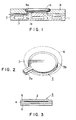
- an improved electrostatic chuck with a specimen wafer A as a work placed thereon includes an electric conductive support body 1 at the bottom of the chuck.
- the support body 1 has, at its center, a round protrusion la with the thickness slightly greater than the rest of the body 1.
- the support body 1 is made of a material with a high conductivity such as copper or aluminum.
- an electrostatic attraction body 3 To the upper surface of the protrusion la of the support body 1 is applied an electrostatic attraction body 3 in which a metallic electrode 2 is accommodated.
- the body 3 comprises an insulator layer and an adhesive layer 6.
- the insulator layer has an insulator base film 4 and a insulator cover film 5.
- the insulator layer is made of an organic resin layer with the thickness of 10 to 100 ⁇ m, such as a polyimide layer or a polyester layer.
- the electrode 2 made of, for example, copper film with the thickness of 10 to 50 ⁇ m.
- the insulator cover film 5 made of polyimide or polyester is applied to the electrode 2, placing the electrode 2 between the insulator cover film 5 and the insulator base film 4. Further, on the bottom of the insulator base film 4 is provided the adhesive layer 6.
- the electrode 2 may be made of a metallic film with the thickness of less than 2 ⁇ m, formed on the insulator base film 4 or the insulator cover film 5 by means of vacuum evaporation or sputtering.
- the thicknesses of both the insulator base film 4 and the insulator cover film 5 are 50 ⁇ m, respectively, the thickness of the copper-made electrode 2 is 18 ⁇ m, the adhesive layer 6 is 40 ⁇ m, and the entire thickness of the electrostatic attraction body 3 amounts to 158 ⁇ m. It is desirable that the body 3 is formed as thin as possible in order to increase heat transmission efficiency.
- Both the electrostatic attraction body 3 and the specimen wafer A have circular shapes, respectively.
- the electrostatic attraction body 3 has an attracting surface slightly smaller than the surface, to be attracted, of the specimen wafer A. A portion of the periphery of the electrostatic attraction body 3 is so projected from its circular main body 3b as to form an electric connection portion 3a for connecting the electrode 2 with an external power supply, not shown.
- the electrostatic chuck according to the present invention is further provided with a cover plate 8 applied onto the support body 1 by means of an adhesive.
- the cover plate 8 has a round aperture 8a at its center for placing the wafer A therein.
- the cover plate 8 can cover the exposed surfaces except the surface of the protrusion la on which the wafer A is placed and is formed of a ceramic material such as carbon, quartz, alumina, silicon carbide (SiC), or silicon nitride (SiN), etc.
- the cover plate 8 may be formed of a heat-resistant synthetic resin such as polyimide or fluoreoresin, etc. Further, the cover plate 8 may be fixed to the support body 1 by means of screws. In addition, the cover plate 8 may be simply placed or clamped upon the support body 1 by means of a clamping member provided on the periphery of the cover means.
- the specimen wafer A in operation, is placed upon the electrostatic attraction body 3, and thereafter a DC voltage is applied to the electrode 2.
- the wafer A is thus attracted by means of electrostatic forces and is secured on the electrostatic attraction body 3.
- the electrostatic chuck described above is placed in a vacuum chamber, and a vacuum process such as etching operation, etc. is carried out for the specimen wafer A.
- cooling water is provided through the channels 7 during the processing.
- a loader mechanism not shown, which is provided through the support body 1 and which is capable of vertically lifting and lowering the wafer A through the support body 1.
- the electrostatic attraction body 3 and the support body 1 are provided with apertures (not shown) to permit the vertical movements of the lifting mechanism, respectively.
- the material of the support body is no longer directly hit by ion beams nor scattered during an etching process. In addition, no impure matters are generated in the vacuum processing chamber.
- the support body 1 is cooled off desirably and consequently the specimen wafer A does not suffer damage due to heat.
- an electrostatic chuck according to a second embodiment of the current invention is shown.
- an annular groove 9 is formed around the entire periphery of the central protrusion la of the support body 1.
- an electrostatic attraction body 3 is fixed to the upper surface of a round protrusion la formed by digging an annular groove 9.
- An electric connection portion 3a is projected from the main body 3b of the attraction body 3 and extended across the groove 9.
- a cover plate 8b and a cover ring 8c are placed, respectively.
- an electrostatic chuck includes an electrostatic attraction body 3 which has an electric connection portion 3a extending downward through the support body 1 for an electrical connection.
- This structure enables the electrostatic chuck to be connected to a power source directly below the support body 3. This construction also ensures to prevent ion beam from attacking the upper surface of the support body 1.
- the electrostatic chuck in accordance with the fourth embodiment of the invention includes a cover ring 8c provided immediately below the adjoining portion of a cover plate 8b and the electrostatic attraction body 3.
- the provision of the cover members 8b, 8c further ensures to prevent ion beam from hitting the upper surface of the support body 1.
- the fourth embodiment also ensures the electrostatic chuck to be connected to a power source directly below the support body 1, as is the case with the third embodiment described above.
- an anodic oxidation process should be carried out on the surface of the support body 1.
- an anodic oxidation layer forms cover means instead of the cover members 8b, 8c.
Landscapes
- Container, Conveyance, Adherence, Positioning, Of Wafer (AREA)
- Jigs For Machine Tools (AREA)
Applications Claiming Priority (2)
| Application Number | Priority Date | Filing Date | Title |
|---|---|---|---|
| JP117493/84 | 1984-07-31 | ||
| JP1984117493U JPS6131636U (ja) | 1984-07-31 | 1984-07-31 | 静電チヤツク |
Publications (3)
| Publication Number | Publication Date |
|---|---|
| EP0171011A2 true EP0171011A2 (fr) | 1986-02-12 |
| EP0171011A3 EP0171011A3 (en) | 1987-08-19 |
| EP0171011B1 EP0171011B1 (fr) | 1989-11-02 |
Family
ID=14713089
Family Applications (1)
| Application Number | Title | Priority Date | Filing Date |
|---|---|---|---|
| EP85109514A Expired EP0171011B1 (fr) | 1984-07-31 | 1985-07-29 | Appareil de maintien électrostatique |
Country Status (4)
| Country | Link |
|---|---|
| US (1) | US4645218A (fr) |
| EP (1) | EP0171011B1 (fr) |
| JP (1) | JPS6131636U (fr) |
| DE (1) | DE3574079D1 (fr) |
Cited By (19)
| Publication number | Priority date | Publication date | Assignee | Title |
|---|---|---|---|---|
| EP0439000A1 (fr) * | 1990-01-25 | 1991-07-31 | Applied Materials, Inc. | Dispositif de serrage électrostatique et procédé |
| DE4107752A1 (de) * | 1990-03-13 | 1991-09-26 | Fuji Electric Co Ltd | Elektrostatische einspannvorrichtung fuer ein scheibenfoermiges substrat |
| EP0452222A1 (fr) * | 1990-04-12 | 1991-10-16 | Commissariat A L'energie Atomique | Porte-substrat électrostatique |
| EP0462563A1 (fr) * | 1990-06-18 | 1991-12-27 | Tokyo Electron Limited | Appareil de traitement pour semi-conducteur |
| EP0486966A1 (fr) * | 1990-11-17 | 1992-05-27 | Tokyo Electron Limited | Appareil de maintien électrostatique |
| EP0491503A3 (fr) * | 1990-12-19 | 1992-07-22 | AT&T Corp. | Procédé pour le dépôt de métal |
| EP0660388A1 (fr) * | 1993-12-20 | 1995-06-28 | International Business Machines Corporation | Procédé de fabrication d'un mandrin électrostatique comprenant une isolation d'oxyde |
| WO1995020838A1 (fr) * | 1994-01-31 | 1995-08-03 | Applied Materials, Inc. | Mandrin electrostatique a film isolant epousant la base |
| EP0666586A1 (fr) * | 1994-01-31 | 1995-08-09 | Applied Materials, Inc. | Un appareil de support pour un substrat pendant le traitement avec un gaz corrosif |
| EP0669644A3 (fr) * | 1994-02-28 | 1995-12-13 | Applied Materials Inc | Support électrostatique. |
| EP0693771A1 (fr) * | 1994-07-18 | 1996-01-24 | Applied Materials, Inc. | Support électrostatique pour substrat dans une chambre de traitement |
| EP0734057A3 (fr) * | 1993-06-07 | 1996-11-20 | Applied Materials, Inc. | Appareil pour éviter la nécessité de nettoyer les bords externes d'une plaque de support |
| US5600530A (en) * | 1992-08-04 | 1997-02-04 | The Morgan Crucible Company Plc | Electrostatic chuck |
| US5729423A (en) * | 1994-01-31 | 1998-03-17 | Applied Materials, Inc. | Puncture resistant electrostatic chuck |
| US5801915A (en) * | 1994-01-31 | 1998-09-01 | Applied Materials, Inc. | Electrostatic chuck having a unidirectionally conducting coupler layer |
| EP0863545A3 (fr) * | 1997-03-06 | 2000-05-31 | Applied Materials, Inc. | Mandrin électrostatique en céramique monocristalline |
| US6278600B1 (en) | 1994-01-31 | 2001-08-21 | Applied Materials, Inc. | Electrostatic chuck with improved temperature control and puncture resistance |
| US6598559B1 (en) | 2000-03-24 | 2003-07-29 | Applied Materials, Inc. | Temperature controlled chamber |
| DE4216218B4 (de) * | 1991-05-17 | 2009-04-02 | Christopher Max Horwitz | Verfahren und Vorrichtung zum elektrostatischen Halten eines Körpers mittels einer elektrostatischen Haltevorrichtung |
Families Citing this family (95)
| Publication number | Priority date | Publication date | Assignee | Title |
|---|---|---|---|---|
| US4724510A (en) * | 1986-12-12 | 1988-02-09 | Tegal Corporation | Electrostatic wafer clamp |
| JPH0634839Y2 (ja) * | 1987-12-18 | 1994-09-14 | ヤンマー農機株式会社 | 背負動力散布機の残量表示装置 |
| US5001594A (en) * | 1989-09-06 | 1991-03-19 | Mcnc | Electrostatic handling device |
| US5224581A (en) * | 1989-12-14 | 1993-07-06 | Applied Materials, Inc. | Magnetic semiconductor wafers with handling apparatus and method |
| US5147828A (en) * | 1989-12-14 | 1992-09-15 | Applied Materials, Inc. | Method of handling magnetic semiconductor wafers |
| US5255153A (en) * | 1990-07-20 | 1993-10-19 | Tokyo Electron Limited | Electrostatic chuck and plasma apparatus equipped therewith |
| DE4026244C2 (de) * | 1990-08-18 | 1996-02-08 | Ant Nachrichtentech | Substratträger |
| US5099571A (en) * | 1990-09-07 | 1992-03-31 | International Business Machines Corporation | Method for fabricating a split-ring electrostatic chuck |
| US5055964A (en) * | 1990-09-07 | 1991-10-08 | International Business Machines Corporation | Electrostatic chuck having tapered electrodes |
| DE69130205T2 (de) * | 1990-12-25 | 1999-03-25 | Ngk Insulators, Ltd., Nagoya, Aichi | Heizungsapparat für eine Halbleiterscheibe und Verfahren zum Herstellen desselben |
| US5166856A (en) * | 1991-01-31 | 1992-11-24 | International Business Machines Corporation | Electrostatic chuck with diamond coating |
| US5155652A (en) * | 1991-05-02 | 1992-10-13 | International Business Machines Corporation | Temperature cycling ceramic electrostatic chuck |
| US5191506A (en) * | 1991-05-02 | 1993-03-02 | International Business Machines Corporation | Ceramic electrostatic chuck |
| US5207437A (en) * | 1991-10-29 | 1993-05-04 | International Business Machines Corporation | Ceramic electrostatic wafer chuck |
| US5539609A (en) * | 1992-12-02 | 1996-07-23 | Applied Materials, Inc. | Electrostatic chuck usable in high density plasma |
| US5350479A (en) * | 1992-12-02 | 1994-09-27 | Applied Materials, Inc. | Electrostatic chuck for high power plasma processing |
| US5382311A (en) * | 1992-12-17 | 1995-01-17 | Tokyo Electron Limited | Stage having electrostatic chuck and plasma processing apparatus using same |
| US5384681A (en) * | 1993-03-01 | 1995-01-24 | Toto Ltd. | Electrostatic chuck |
| US5662770A (en) | 1993-04-16 | 1997-09-02 | Micron Technology, Inc. | Method and apparatus for improving etch uniformity in remote source plasma reactors with powered wafer chucks |
| JPH06326175A (ja) * | 1993-04-22 | 1994-11-25 | Applied Materials Inc | 集積回路処理装置において使用されるウエハサポートの誘電材への保護被覆とその形成方法 |
| TW277139B (fr) | 1993-09-16 | 1996-06-01 | Hitachi Seisakusyo Kk | |
| TW288253B (fr) * | 1994-02-03 | 1996-10-11 | Aneruba Kk | |
| US5581874A (en) * | 1994-03-28 | 1996-12-10 | Tokyo Electron Limited | Method of forming a bonding portion |
| US5521790A (en) * | 1994-05-12 | 1996-05-28 | International Business Machines Corporation | Electrostatic chuck having relatively thick and thin areas and means for uniformly cooling said thick and thin areas during chuck anodization |
| JP3208029B2 (ja) * | 1994-11-22 | 2001-09-10 | 株式会社巴川製紙所 | 静電チャック装置およびその作製方法 |
| US5792562A (en) * | 1995-01-12 | 1998-08-11 | Applied Materials, Inc. | Electrostatic chuck with polymeric impregnation and method of making |
| US5691876A (en) * | 1995-01-31 | 1997-11-25 | Applied Materials, Inc. | High temperature polyimide electrostatic chuck |
| US5671116A (en) * | 1995-03-10 | 1997-09-23 | Lam Research Corporation | Multilayered electrostatic chuck and method of manufacture thereof |
| US5673922A (en) * | 1995-03-13 | 1997-10-07 | Applied Materials, Inc. | Apparatus for centering substrates on support members |
| US5835333A (en) * | 1995-10-30 | 1998-11-10 | Lam Research Corporation | Negative offset bipolar electrostatic chucks |
| US5796074A (en) * | 1995-11-28 | 1998-08-18 | Applied Materials, Inc. | Wafer heater assembly |
| US5891348A (en) * | 1996-01-26 | 1999-04-06 | Applied Materials, Inc. | Process gas focusing apparatus and method |
| US5812361A (en) * | 1996-03-29 | 1998-09-22 | Lam Research Corporation | Dynamic feedback electrostatic wafer chuck |
| US6108189A (en) * | 1996-04-26 | 2000-08-22 | Applied Materials, Inc. | Electrostatic chuck having improved gas conduits |
| US5751537A (en) * | 1996-05-02 | 1998-05-12 | Applied Materials, Inc. | Multielectrode electrostatic chuck with fuses |
| US6055150A (en) * | 1996-05-02 | 2000-04-25 | Applied Materials, Inc. | Multi-electrode electrostatic chuck having fuses in hollow cavities |
| US5748434A (en) * | 1996-06-14 | 1998-05-05 | Applied Materials, Inc. | Shield for an electrostatic chuck |
| KR100290264B1 (ko) * | 1997-01-22 | 2001-09-22 | 호소이 쇼지로 | 정전처크장치 및 그 제조방법 |
| US5942039A (en) * | 1997-05-01 | 1999-08-24 | Applied Materials, Inc. | Self-cleaning focus ring |
| US5900064A (en) * | 1997-05-01 | 1999-05-04 | Applied Materials, Inc. | Plasma process chamber |
| US5978202A (en) * | 1997-06-27 | 1999-11-02 | Applied Materials, Inc. | Electrostatic chuck having a thermal transfer regulator pad |
| US6034863A (en) * | 1997-11-12 | 2000-03-07 | Applied Materials, Inc. | Apparatus for retaining a workpiece in a process chamber within a semiconductor wafer processing system |
| US5901030A (en) * | 1997-12-02 | 1999-05-04 | Dorsey Gage, Inc. | Electrostatic chuck employing thermoelectric cooling |
| US5969934A (en) * | 1998-04-10 | 1999-10-19 | Varian Semiconductor Equipment Associats, Inc. | Electrostatic wafer clamp having low particulate contamination of wafers |
| US6104596A (en) * | 1998-04-21 | 2000-08-15 | Applied Materials, Inc. | Apparatus for retaining a subtrate in a semiconductor wafer processing system and a method of fabricating same |
| US6238160B1 (en) * | 1998-12-02 | 2001-05-29 | Taiwan Semiconductor Manufacturing Company, Ltd' | Method for transporting and electrostatically chucking a semiconductor wafer or the like |
| US6263829B1 (en) | 1999-01-22 | 2001-07-24 | Applied Materials, Inc. | Process chamber having improved gas distributor and method of manufacture |
| US6159299A (en) * | 1999-02-09 | 2000-12-12 | Applied Materials, Inc. | Wafer pedestal with a purge ring |
| US6490146B2 (en) | 1999-05-07 | 2002-12-03 | Applied Materials Inc. | Electrostatic chuck bonded to base with a bond layer and method |
| US6462928B1 (en) | 1999-05-07 | 2002-10-08 | Applied Materials, Inc. | Electrostatic chuck having improved electrical connector and method |
| US6310755B1 (en) | 1999-05-07 | 2001-10-30 | Applied Materials, Inc. | Electrostatic chuck having gas cavity and method |
| US6466426B1 (en) * | 1999-08-03 | 2002-10-15 | Applied Materials Inc. | Method and apparatus for thermal control of a semiconductor substrate |
| US6839217B1 (en) | 1999-10-01 | 2005-01-04 | Varian Semiconductor Equipment Associates, Inc. | Surface structure and method of making, and electrostatic wafer clamp incorporating surface structure |
| US6538873B1 (en) | 1999-11-02 | 2003-03-25 | Varian Semiconductor Equipment Associates, Inc. | Active electrostatic seal and electrostatic vacuum pump |
| US6362946B1 (en) | 1999-11-02 | 2002-03-26 | Varian Semiconductor Equipment Associates, Inc. | Electrostatic wafer clamp having electrostatic seal for retaining gas |
| US6490144B1 (en) | 1999-11-29 | 2002-12-03 | Applied Materials, Inc. | Support for supporting a substrate in a process chamber |
| JP4753460B2 (ja) * | 2000-08-16 | 2011-08-24 | 株式会社クリエイティブ テクノロジー | 静電チャック及びその製造方法 |
| FR2818050B1 (fr) * | 2000-12-12 | 2006-08-11 | Semco Engineering Sa | Dispositif de prehension electrostatique d'une tranche de composant electronique |
| US6581275B2 (en) | 2001-01-22 | 2003-06-24 | Applied Materials Inc. | Fabricating an electrostatic chuck having plasma resistant gas conduits |
| US6554954B2 (en) * | 2001-04-03 | 2003-04-29 | Applied Materials Inc. | Conductive collar surrounding semiconductor workpiece in plasma chamber |
| US6682627B2 (en) | 2001-09-24 | 2004-01-27 | Applied Materials, Inc. | Process chamber having a corrosion-resistant wall and method |
| US6538872B1 (en) | 2001-11-05 | 2003-03-25 | Applied Materials, Inc. | Electrostatic chuck having heater and method |
| US20030188685A1 (en) * | 2002-04-08 | 2003-10-09 | Applied Materials, Inc. | Laser drilled surfaces for substrate processing chambers |
| US7275577B2 (en) * | 2002-11-16 | 2007-10-02 | Lg.Philips Lcd Co., Ltd. | Substrate bonding machine for liquid crystal display device |
| US20060175772A1 (en) * | 2003-03-19 | 2006-08-10 | Tokyo Electron Limited | Substrate holding mechanism using electrostaic chuck and method of manufacturing the same |
| US20040226516A1 (en) * | 2003-05-13 | 2004-11-18 | Daniel Timothy J. | Wafer pedestal cover |
| US20040244949A1 (en) * | 2003-05-30 | 2004-12-09 | Tokyo Electron Limited | Temperature controlled shield ring |
| US7910218B2 (en) | 2003-10-22 | 2011-03-22 | Applied Materials, Inc. | Cleaning and refurbishing chamber components having metal coatings |
| US7697260B2 (en) * | 2004-03-31 | 2010-04-13 | Applied Materials, Inc. | Detachable electrostatic chuck |
| US20060023395A1 (en) * | 2004-07-30 | 2006-02-02 | Taiwan Semiconductor Manufacturing Co., Ltd. | Systems and methods for temperature control of semiconductor wafers |
| US7670436B2 (en) | 2004-11-03 | 2010-03-02 | Applied Materials, Inc. | Support ring assembly |
| US8617672B2 (en) | 2005-07-13 | 2013-12-31 | Applied Materials, Inc. | Localized surface annealing of components for substrate processing chambers |
| US20070029046A1 (en) * | 2005-08-04 | 2007-02-08 | Applied Materials, Inc. | Methods and systems for increasing substrate temperature in plasma reactors |
| US7762114B2 (en) * | 2005-09-09 | 2010-07-27 | Applied Materials, Inc. | Flow-formed chamber component having a textured surface |
| US9127362B2 (en) | 2005-10-31 | 2015-09-08 | Applied Materials, Inc. | Process kit and target for substrate processing chamber |
| US8647484B2 (en) * | 2005-11-25 | 2014-02-11 | Applied Materials, Inc. | Target for sputtering chamber |
| US20070283891A1 (en) * | 2006-03-29 | 2007-12-13 | Nobuyuki Okayama | Table for supporting substrate, and vacuum-processing equipment |
| US8226769B2 (en) * | 2006-04-27 | 2012-07-24 | Applied Materials, Inc. | Substrate support with electrostatic chuck having dual temperature zones |
| US20070283884A1 (en) * | 2006-05-30 | 2007-12-13 | Applied Materials, Inc. | Ring assembly for substrate processing chamber |
| US9275887B2 (en) | 2006-07-20 | 2016-03-01 | Applied Materials, Inc. | Substrate processing with rapid temperature gradient control |
| US20080073032A1 (en) * | 2006-08-10 | 2008-03-27 | Akira Koshiishi | Stage for plasma processing apparatus, and plasma processing apparatus |
| US7589950B2 (en) * | 2006-10-13 | 2009-09-15 | Applied Materials, Inc. | Detachable electrostatic chuck having sealing assembly |
| US7981262B2 (en) | 2007-01-29 | 2011-07-19 | Applied Materials, Inc. | Process kit for substrate processing chamber |
| US7942969B2 (en) * | 2007-05-30 | 2011-05-17 | Applied Materials, Inc. | Substrate cleaning chamber and components |
| US20090084317A1 (en) * | 2007-09-28 | 2009-04-02 | Applied Materials, Inc. | Atomic layer deposition chamber and components |
| JP2009188332A (ja) * | 2008-02-08 | 2009-08-20 | Tokyo Electron Ltd | プラズマ処理装置用基板載置台、プラズマ処理装置および絶縁皮膜の成膜方法 |
| US8405005B2 (en) * | 2009-02-04 | 2013-03-26 | Mattson Technology, Inc. | Electrostatic chuck system and process for radially tuning the temperature profile across the surface of a substrate |
| NL2008630A (en) * | 2011-04-27 | 2012-10-30 | Asml Netherlands Bv | Substrate holder, lithographic apparatus, device manufacturing method, and method of manufacturing a substrate holder. |
| US10208884B2 (en) | 2014-01-30 | 2019-02-19 | Draingarde, Inc. | Watershed protection device and system |
| USD768843S1 (en) | 2014-11-28 | 2016-10-11 | Draingarde Inc. | Catch basin cover |
| CN107924816B (zh) | 2015-06-26 | 2021-08-31 | 东京毅力科创株式会社 | 具有含硅减反射涂层或硅氧氮化物相对于不同膜或掩模的可控蚀刻选择性的气相蚀刻 |
| KR20180014207A (ko) | 2015-06-26 | 2018-02-07 | 도쿄엘렉트론가부시키가이샤 | 기상 식각 시스템 및 방법 |
| JP7012454B2 (ja) * | 2017-04-27 | 2022-01-28 | 株式会社岡本工作機械製作所 | 静電吸着チャックの製造方法並びに半導体装置の製造方法 |
| DE102018116463A1 (de) * | 2018-07-06 | 2020-01-09 | Berliner Glas Kgaa Herbert Kubatz Gmbh & Co. | Elektrostatische Haltevorrichtung und Verfahren zu deren Herstellung |
| TWD223375S (zh) * | 2021-03-29 | 2023-02-01 | 大陸商北京北方華創微電子裝備有限公司 | 靜電卡盤 |
Family Cites Families (7)
| Publication number | Priority date | Publication date | Assignee | Title |
|---|---|---|---|---|
| GB1443215A (en) * | 1973-11-07 | 1976-07-21 | Mullard Ltd | Electrostatically clamping a semiconductor wafer during device manufacture |
| US4184188A (en) * | 1978-01-16 | 1980-01-15 | Veeco Instruments Inc. | Substrate clamping technique in IC fabrication processes |
| JPS5685828A (en) * | 1979-12-17 | 1981-07-13 | Nec Corp | Electrostatic wafer holder |
| US4384918A (en) * | 1980-09-30 | 1983-05-24 | Fujitsu Limited | Method and apparatus for dry etching and electrostatic chucking device used therein |
| GB2106325A (en) * | 1981-09-14 | 1983-04-07 | Philips Electronic Associated | Electrostatic chuck |
| JPS58190037A (ja) * | 1982-04-28 | 1983-11-05 | Toshiba Corp | 静電チヤツク装置およびその製造方法 |
| GB2154365A (en) * | 1984-02-10 | 1985-09-04 | Philips Electronic Associated | Loading semiconductor wafers on an electrostatic chuck |
-
1984
- 1984-07-31 JP JP1984117493U patent/JPS6131636U/ja active Pending
-
1985
- 1985-07-29 DE DE8585109514T patent/DE3574079D1/de not_active Expired
- 1985-07-29 EP EP85109514A patent/EP0171011B1/fr not_active Expired
- 1985-07-30 US US06/760,512 patent/US4645218A/en not_active Expired - Lifetime
Cited By (34)
| Publication number | Priority date | Publication date | Assignee | Title |
|---|---|---|---|---|
| EP0439000A1 (fr) * | 1990-01-25 | 1991-07-31 | Applied Materials, Inc. | Dispositif de serrage électrostatique et procédé |
| US5160152A (en) * | 1990-03-13 | 1992-11-03 | Fuji Electric Co., Ltd. | Electrostatic chuck |
| DE4107752A1 (de) * | 1990-03-13 | 1991-09-26 | Fuji Electric Co Ltd | Elektrostatische einspannvorrichtung fuer ein scheibenfoermiges substrat |
| GB2243022A (en) * | 1990-03-13 | 1991-10-16 | Fuji Electric Co Ltd | Electrostatic chucks |
| DE4107752C2 (de) * | 1990-03-13 | 2003-04-24 | Fuji Electric Co Ltd | Elektrostatische Einspannvorrichtung für ein scheibenförmiges Substrat |
| GB2243022B (en) * | 1990-03-13 | 1994-07-20 | Fuji Electric Co Ltd | Electrostatic chuck |
| FR2661039A1 (fr) * | 1990-04-12 | 1991-10-18 | Commissariat Energie Atomique | Porte-substrat electrostatique. |
| EP0452222A1 (fr) * | 1990-04-12 | 1991-10-16 | Commissariat A L'energie Atomique | Porte-substrat électrostatique |
| EP0462563A1 (fr) * | 1990-06-18 | 1991-12-27 | Tokyo Electron Limited | Appareil de traitement pour semi-conducteur |
| EP0486966A1 (fr) * | 1990-11-17 | 1992-05-27 | Tokyo Electron Limited | Appareil de maintien électrostatique |
| US5539179A (en) * | 1990-11-17 | 1996-07-23 | Tokyo Electron Limited | Electrostatic chuck having a multilayer structure for attracting an object |
| EP0491503A3 (fr) * | 1990-12-19 | 1992-07-22 | AT&T Corp. | Procédé pour le dépôt de métal |
| US6136159A (en) * | 1990-12-19 | 2000-10-24 | Lucent Technologies Inc. | Method for depositing metal |
| US5807760A (en) * | 1990-12-19 | 1998-09-15 | Lucent Technologies Inc. | Method of despositing an aluminum-rich layer |
| DE4216218B4 (de) * | 1991-05-17 | 2009-04-02 | Christopher Max Horwitz | Verfahren und Vorrichtung zum elektrostatischen Halten eines Körpers mittels einer elektrostatischen Haltevorrichtung |
| US5600530A (en) * | 1992-08-04 | 1997-02-04 | The Morgan Crucible Company Plc | Electrostatic chuck |
| EP0734057A3 (fr) * | 1993-06-07 | 1996-11-20 | Applied Materials, Inc. | Appareil pour éviter la nécessité de nettoyer les bords externes d'une plaque de support |
| EP0660388A1 (fr) * | 1993-12-20 | 1995-06-28 | International Business Machines Corporation | Procédé de fabrication d'un mandrin électrostatique comprenant une isolation d'oxyde |
| US6278600B1 (en) | 1994-01-31 | 2001-08-21 | Applied Materials, Inc. | Electrostatic chuck with improved temperature control and puncture resistance |
| EP0666586A1 (fr) * | 1994-01-31 | 1995-08-09 | Applied Materials, Inc. | Un appareil de support pour un substrat pendant le traitement avec un gaz corrosif |
| WO1995020838A1 (fr) * | 1994-01-31 | 1995-08-03 | Applied Materials, Inc. | Mandrin electrostatique a film isolant epousant la base |
| US5729423A (en) * | 1994-01-31 | 1998-03-17 | Applied Materials, Inc. | Puncture resistant electrostatic chuck |
| US5745331A (en) * | 1994-01-31 | 1998-04-28 | Applied Materials, Inc. | Electrostatic chuck with conformal insulator film |
| US5753132A (en) * | 1994-01-31 | 1998-05-19 | Applied Materials, Inc. | Method of making electrostatic chuck with conformal insulator film |
| US5801915A (en) * | 1994-01-31 | 1998-09-01 | Applied Materials, Inc. | Electrostatic chuck having a unidirectionally conducting coupler layer |
| US5986875A (en) * | 1994-01-31 | 1999-11-16 | Applied Materials, Inc. | Puncture resistant electrostatic chuck |
| EP0669644A3 (fr) * | 1994-02-28 | 1995-12-13 | Applied Materials Inc | Support électrostatique. |
| US5634266A (en) * | 1994-02-28 | 1997-06-03 | Applied Materials Inc. | Method of making a dielectric chuck |
| US5671117A (en) * | 1994-02-28 | 1997-09-23 | Applied Materials Inc. | Electrostatic chuck |
| EP0693771A1 (fr) * | 1994-07-18 | 1996-01-24 | Applied Materials, Inc. | Support électrostatique pour substrat dans une chambre de traitement |
| US5606485A (en) * | 1994-07-18 | 1997-02-25 | Applied Materials, Inc. | Electrostatic chuck having improved erosion resistance |
| EP0863545A3 (fr) * | 1997-03-06 | 2000-05-31 | Applied Materials, Inc. | Mandrin électrostatique en céramique monocristalline |
| US6529362B2 (en) | 1997-03-06 | 2003-03-04 | Applied Materials Inc. | Monocrystalline ceramic electrostatic chuck |
| US6598559B1 (en) | 2000-03-24 | 2003-07-29 | Applied Materials, Inc. | Temperature controlled chamber |
Also Published As
| Publication number | Publication date |
|---|---|
| DE3574079D1 (en) | 1989-12-07 |
| US4645218A (en) | 1987-02-24 |
| JPS6131636U (ja) | 1986-02-26 |
| EP0171011A3 (en) | 1987-08-19 |
| EP0171011B1 (fr) | 1989-11-02 |
Similar Documents
| Publication | Publication Date | Title |
|---|---|---|
| EP0171011B1 (fr) | Appareil de maintien électrostatique | |
| US6238513B1 (en) | Wafer lift assembly | |
| US5969934A (en) | Electrostatic wafer clamp having low particulate contamination of wafers | |
| JP3129452B2 (ja) | 静電チャック | |
| EP0439000B1 (fr) | Dispositif de serrage électrostatique et procédé | |
| US5631803A (en) | Erosion resistant electrostatic chuck with improved cooling system | |
| US5345999A (en) | Method and apparatus for cooling semiconductor wafers | |
| US5740009A (en) | Apparatus for improving wafer and chuck edge protection | |
| KR100807136B1 (ko) | 플라즈마 챔버에서 유용한 정전 에지 링 척을 포함하는 커플링 링 어셈블리 및 플라즈마 챔버를 사용하여 반도체 기판을 처리하는 방법 | |
| US5996218A (en) | Method of forming an electrostatic chuck suitable for magnetic flux processing | |
| EP0840434A2 (fr) | Structure topographique améliorée d'un mandrin électrostatique et procédé de fabrication | |
| JPH0718438A (ja) | 静電チャック装置 | |
| US5830808A (en) | Plasma reactor with magnet for protecting an electroacoustic chuck from the plasma | |
| CN110931415B (zh) | 支撑件 | |
| US20030089457A1 (en) | Apparatus for controlling a thermal conductivity profile for a pedestal in a semiconductor wafer processing chamber | |
| JP2001523045A (ja) | 加工物を保持する装置 | |
| US6195246B1 (en) | Electrostatic chuck having replaceable dielectric cover | |
| JP2767282B2 (ja) | 基板保持装置 | |
| KR20030047341A (ko) | 이온주입장치의 정전척 | |
| JP3769378B2 (ja) | 静電チャック | |
| EP0742579A2 (fr) | Une méthode et appareil servant à la concentration de plasma sur une surface d'un substrat pendant le traitement | |
| JPH07176603A (ja) | 基板保持装置 | |
| JPS6156843A (ja) | 静電吸着板 | |
| JPH0225987B2 (fr) | ||
| JP2000113850A (ja) | 基板保持装置 |
Legal Events
| Date | Code | Title | Description |
|---|---|---|---|
| PUAI | Public reference made under article 153(3) epc to a published international application that has entered the european phase |
Free format text: ORIGINAL CODE: 0009012 |
|
| AK | Designated contracting states |
Designated state(s): DE FR GB |
|
| RAP1 | Party data changed (applicant data changed or rights of an application transferred) |
Owner name: KABUSHIKI KAISHA TOKUDA SEISAKUSHO |
|
| PUAL | Search report despatched |
Free format text: ORIGINAL CODE: 0009013 |
|
| AK | Designated contracting states |
Kind code of ref document: A3 Designated state(s): DE FR GB |
|
| 17P | Request for examination filed |
Effective date: 19871111 |
|
| 17Q | First examination report despatched |
Effective date: 19880311 |
|
| GRAA | (expected) grant |
Free format text: ORIGINAL CODE: 0009210 |
|
| AK | Designated contracting states |
Kind code of ref document: B1 Designated state(s): DE FR GB |
|
| REF | Corresponds to: |
Ref document number: 3574079 Country of ref document: DE Date of ref document: 19891207 |
|
| ET | Fr: translation filed | ||
| PLBE | No opposition filed within time limit |
Free format text: ORIGINAL CODE: 0009261 |
|
| STAA | Information on the status of an ep patent application or granted ep patent |
Free format text: STATUS: NO OPPOSITION FILED WITHIN TIME LIMIT |
|
| 26N | No opposition filed | ||
| REG | Reference to a national code |
Ref country code: GB Ref legal event code: 732E |
|
| REG | Reference to a national code |
Ref country code: FR Ref legal event code: TP |
|
| REG | Reference to a national code |
Ref country code: GB Ref legal event code: IF02 |
|
| PGFP | Annual fee paid to national office [announced via postgrant information from national office to epo] |
Ref country code: GB Payment date: 20030723 Year of fee payment: 19 |
|
| PGFP | Annual fee paid to national office [announced via postgrant information from national office to epo] |
Ref country code: FR Payment date: 20030729 Year of fee payment: 19 |
|
| PGFP | Annual fee paid to national office [announced via postgrant information from national office to epo] |
Ref country code: DE Payment date: 20030807 Year of fee payment: 19 |
|
| PG25 | Lapsed in a contracting state [announced via postgrant information from national office to epo] |
Ref country code: GB Free format text: LAPSE BECAUSE OF NON-PAYMENT OF DUE FEES Effective date: 20040729 |
|
| PG25 | Lapsed in a contracting state [announced via postgrant information from national office to epo] |
Ref country code: DE Free format text: LAPSE BECAUSE OF NON-PAYMENT OF DUE FEES Effective date: 20050201 |
|
| GBPC | Gb: european patent ceased through non-payment of renewal fee |
Effective date: 20040729 |
|
| PG25 | Lapsed in a contracting state [announced via postgrant information from national office to epo] |
Ref country code: FR Free format text: LAPSE BECAUSE OF NON-PAYMENT OF DUE FEES Effective date: 20050331 |
|
| REG | Reference to a national code |
Ref country code: FR Ref legal event code: ST |