EP0173466A2 - Mikrobefehlsteuerung - Google Patents
Mikrobefehlsteuerung Download PDFInfo
- Publication number
- EP0173466A2 EP0173466A2 EP85305442A EP85305442A EP0173466A2 EP 0173466 A2 EP0173466 A2 EP 0173466A2 EP 85305442 A EP85305442 A EP 85305442A EP 85305442 A EP85305442 A EP 85305442A EP 0173466 A2 EP0173466 A2 EP 0173466A2
- Authority
- EP
- European Patent Office
- Prior art keywords
- parameters
- microprogram
- phase
- phases
- instruction
- Prior art date
- Legal status (The legal status is an assumption and is not a legal conclusion. Google has not performed a legal analysis and makes no representation as to the accuracy of the status listed.)
- Granted
Links
Images


Classifications
-
- G—PHYSICS
- G06—COMPUTING OR CALCULATING; COUNTING
- G06F—ELECTRIC DIGITAL DATA PROCESSING
- G06F9/00—Arrangements for program control, e.g. control units
- G06F9/06—Arrangements for program control, e.g. control units using stored programs, i.e. using an internal store of processing equipment to receive or retain programs
- G06F9/22—Microcontrol or microprogram arrangements
- G06F9/28—Enhancement of operational speed, e.g. by using several microcontrol devices operating in parallel
-
- G—PHYSICS
- G06—COMPUTING OR CALCULATING; COUNTING
- G06F—ELECTRIC DIGITAL DATA PROCESSING
- G06F9/00—Arrangements for program control, e.g. control units
- G06F9/06—Arrangements for program control, e.g. control units using stored programs, i.e. using an internal store of processing equipment to receive or retain programs
- G06F9/22—Microcontrol or microprogram arrangements
- G06F9/223—Execution means for microinstructions irrespective of the microinstruction function, e.g. decoding of microinstructions and nanoinstructions; timing of microinstructions; programmable logic arrays; delays and fan-out problems
-
- G—PHYSICS
- G06—COMPUTING OR CALCULATING; COUNTING
- G06F—ELECTRIC DIGITAL DATA PROCESSING
- G06F9/00—Arrangements for program control, e.g. control units
- G06F9/06—Arrangements for program control, e.g. control units using stored programs, i.e. using an internal store of processing equipment to receive or retain programs
- G06F9/30—Arrangements for executing machine instructions, e.g. instruction decode
- G06F9/30181—Instruction operation extension or modification
-
- G—PHYSICS
- G06—COMPUTING OR CALCULATING; COUNTING
- G06F—ELECTRIC DIGITAL DATA PROCESSING
- G06F9/00—Arrangements for program control, e.g. control units
- G06F9/06—Arrangements for program control, e.g. control units using stored programs, i.e. using an internal store of processing equipment to receive or retain programs
- G06F9/30—Arrangements for executing machine instructions, e.g. instruction decode
- G06F9/30181—Instruction operation extension or modification
- G06F9/30196—Instruction operation extension or modification using decoder, e.g. decoder per instruction set, adaptable or programmable decoders
Definitions
- This invention relates to microprogram control and, more specifically, is concerned with microprogram controlled data processing apparatus.
- United States Patent No. 3979729 describes a data processing apparatus in which each machine-level instruction is divided into a number of phases, such as operand address formation, operand fetch, and execute, and each of these phases is implemented by means of a suitable microprogram sequence.
- An advantage of dividing the instruction into phases is that, in many cases, the same microprogram sequence can be used for corresponding phases of two or more different instructions; this reduces the number of different microprogram sequences required and hence reduces the overall size of the microprogram.
- a number of different machine instructions may require the address of the operand to be generated in the same way, e.g. by adding a value to a particular base register, and hence these instructions can all share the same microprogram sequence for the address generation phase.
- British Patent Specification No. 1433076 shows a microprogrammed data processing system in which machine-level instructions (macroinstructions) are executed by sequences of microinstructions, and in which each microinstruction is modified by data derived from the machine-level instruction. In this way, the same sequence of microinstructions can be shared between a number of different machine-level instructions. This also reduces the total number of different microprogram sequences required.
- the object of the present invention is therefore to provide a way of reducing the size of a microprogram still.further, without loss of flexibility in the system.
- the invention provides a microprogram controlled data processing apparatus in which machine-level instructions are divided into a plurality of phases, each phase being executed by a sequence of microinstructions, the apparatus comprising: means for producing a plurality of microprogram parameters, means for selecting a predetermined subset of the parameters for each phase, and means for combining the selected parameters with the microinstructions to generate control signals for the apparatus.
- the parameters qualify the effects of the microinstructions, so that the same microprogram sequence can perform different actions in different instructions.
- the operand address generation phases of two instructions may be the same except that one instruction uses one base register whereas the other uses a different base register.
- both these instructions can be handled by means of a single microprogram sequence, which receives the identity of the required base register as a parameter.
- the invention also allows the microinstruction width (i.e. the number of bits in each microinstruction) to be reduced, since some of the necessary contol information is provided by the parameters instead of by microinstructions.
- the parameters may, for example, be derived from the current machine-level instruction.
- the apparatus comprises a plurality of separate functional units, each unit having a separate microprogram store and decoder associated with it, and the parameters are fed to all the decoders in parallel over a parameter bus.
- the processing apparatus to be described is a microprogrammed processor designed to obey the ICL 2900 order code (i.e. machine-level instructions) and is constructed as a single VLSI chip. Details of the 2900 order code are described in "The ICL 2900 series" by J.K.Buckle, published by the Macmillan Press Ltd, 1978.
- the processor comprises a number of functional units, constituting the main data flow 10 of the unit.
- These functional units include a register file 11, working store 12, shifter 13 and arithmetic and logic unit (ALU) 14.
- the working store 11 contains certain registers used by the order code, including a local name base register (LNB), extra name base register (XNB), program counter (PC), linkage table base (LTB), top-of-stack register (TOS), accumulator (ACC), and descriptor register (DR).
- LNB local name base register
- XNB extra name base register
- PC program counter
- LTB linkage table base
- TOS top-of-stack register
- ACC accumulator
- DR descriptor register
- Each of the functional units has a separate microprogram read-only memory (ROM) 15 and local decoder 16 associated with it, in close physical proximity on the chip.
- ROM read-only memory
- This layout facilitates an orderly design of the chip, avoiding unnecessary crossovers of signal lines. All the ROMs 15 are addressed in parallel by a microprogram address from a microprogram sequencer circuit 17, so as to read out a microinstruction from each of the ROMs 15 in parallel.
- the functional units 11-14, the ROMs 15, the decoders 16 and the microprogram sequencer 17 may all be conventional in construction and operation and so need not be described further herein.
- the processor has an instruction register 18 which holds the machine-level instruction currently being executed. The execution of each instruction is broken down into a number of phases, and each of these phases is executed by a particular sequence of microinstructions held in the ROMs 15.
- phase control unit 19 As will be described in detail below with reference to Figure 2, this unit is a finite-state machine having a discrete state for each instruction phase. In each state, the unit 19 produces a set of PHASE signals, which indicate the current phase to be executed. These signals are applied to a look-up table 20, to read out the microprogram start address for this phase. The start address is fed to the microprogram sequencer 17, so as to initiate the corresponding sequence of microinstructions.
- the sequencer 17 When the last microinstruction in a sequence is executed, the sequencer 17 produces a STEP signal. This is applied to the phase control unit 19 and causes it to step on to its next state, thereby initiating the next phase of execution.
- the contents of the instruction register 18 are decoded by a decoder 21, to produce a set of steering signals for the phase control unit 19.
- these signals indicate the type of instruction (read, write, jump etc.) and type of operand (literal, register, virtual etc.) associated with the instruction. These signals are used to steer the phase control unit to its next state at each STEP signal.
- the phase control unit will be steered through a predetermined succession of states, corresponding to the sequence of phases required to execute the instruction.
- the contents of the instruction register 18 are also decoded by another decoder 22 to produce a set of microprogram parameters. These parameters are applied to a parameter selection circuit 23.
- the parameter selection circuit 23 is controlled by the PHASE signals from the phase control unit 19, so as to select a predetermined combination of the parameters in each phase. In general, a different sub-set . of parameters is selected in each phase although in some cases different phases may share the same parameters.
- the selected parameters are applied to a bus 24 which broadcasts them to all the decoders 16 in parallel.
- Each decoder 16 decodes the microinstruction received from the corresponding ROM 15, in combination with the parameters on the bus 24, to produce a set of control signals for the corresponding functional unit 11-14. It can be seen that the parameters modify the effects of the microinstructions, thereby enabling a single microprogram sequence to be used for different phases.
- the unit comprises flip-flops (bistable circuits) FF1-FF13. At any given instant, only one of these flip-flops is set, the others all being unset. Each flip-flop, when set, signifies a particular instruction execution phase, as follows:
- the outputs of the flip-flops represent the PHASE signals mentioned above which define the current phase of execution. As described above, these PHASE signals are used to select the appropriate microprogram sequence for executing the phase in question. They also control the parameter selection circuit 23 to select the appropriate microprogram parameters for this phase. Details of the microprogram sequences form no part of the present invention and so need not be described herein.
- the flip-flops FFl-FF13 are interconnected by AND gates A1-A15 and OR gates 01-05 as shown, to form a finite state machine.
- the AND gates also receive the steering signals from the decoder 21.
- an instruction that performs a direct write to an operand specified by a virtual address will be decoded to produce signals W and VA; all the other steering signals will be false.
- the phase control unit also receives a further steering signal SUCC which indicates a successful jump, i.e. that the jump condition specified in the case of a conditional jump instruction is satisfied. This is derived from a conventional condition testing circuit, not shown.
- Each of the flip-flops FF1-FF13 is clocked by the STEP signal from the microprogram sequencer 17. It can be seen that, at each STEP signal, the output of the currently set flip-flop, in combination with the steering signals, causes another one of the flip-flops to be set; at the same time, the first flip-flop is reset. This steps the phase control unit to a new state, so as to indicate the next phase of execution. For any given instruction, the unit is stepped through a succession of states, indicating the successive phases of that instruction.
- the flip-flop FF3 is set. This initiates the PRIMARY ADDRESS phase.
- the microprogram adds a displacement value N, derived from a predetermined field of the instruction register 18, to a specified base register LNB, XNB, PC or LTB, to form the operand address.
- the gate A8 Since W is false, the gate A8 is now enabled. Hence, at the next STEP signal, the flip-flop FF4 is set. This initiates the PRIMARY READ phase, in which the operand is read, using the address calculated in the previous phase.
- the flip-flop PF11 is set. This initiates the READ EXECUTE phase, in which a specified computational operation (e.g. add, subtract, compare, shift etc.) is performed on the operand and the result placed in a specified register.
- a specified computational operation e.g. add, subtract, compare, shift etc.
- flip-flop FF13 is set again. This initiates the END INSTRUCTION phase, in which the next machine-level instruction, at the address indicated by the program counter PC, is fetched and placed in the instruction register 18.
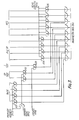
- the circuit receives a set of microprogram parameters, derived from the current machine-level instruction, from the decoder 22. These parameters include the following:
- the parameter selection circuit consists of a number of sets of AND gates A31-A35, controlled by the PHASE signals from the phase control unit 19. Whenever one of these sets of AND gates is enabled, the corresponding parameter is applied to predetermined lines of the parameter bus 24.
- the AND gates A31 are enabled, causing the parameter BASE to be applied to the parameter bus. This is used by the microprogram to select the appropriate base register for calculating the operand address.
- the AND gates A32 are enabled, causing OP SIZE to be applied to the bus. This is used to check for address range violations.
- OP SIZE is again applied to the parameter bus, and is used by the microprogram to determine the number of words to be read from the main store.
- gate A33 is enabled, which causes I SIZE to be applied to the bus. This is used to control the amount by which the program counter is incremented to give the next instruction address.
- the parameters ALU OP and REG are applied to the parameter bus to control the ALU operation in this phase.
- the number of lines making up the parameter bus is determined by the maximum number of bits required to specify the parameters for any one phase. For example, if no phase requires more than sixteen parameter bits, then the parameter bus can comprise just sixteen wires.
- the parameters for one phase can be placed on the same lines as those for another phase if required. For example, in this case, the four bits indicating the arithmetic operation in the READ EXECUTE phase occupy the same bus lines as those used to specify the base register in the PRIMARY ADDRESS phase.
- each phase of the machine-level instruction is executed by a sequence of microinstructions held in the ROMs 15.
- a separate microprogram sequence for each variant of a particular phase; for example, there would be a number of different microprogram sequences for the PRIMARY ADDRESS phase, one for each possible base register.
- a single microprogram sequence is able to handle all variations of a particular phase. For example, a single sequence deals with all the variants of the PRIMARY ADDRESS phase; the sequence merely specifies that some base register is to be used, the choice of the base register being determined by the parameter which appears on the parameter bus during this phase.
Landscapes
- Engineering & Computer Science (AREA)
- Software Systems (AREA)
- Theoretical Computer Science (AREA)
- Physics & Mathematics (AREA)
- General Engineering & Computer Science (AREA)
- General Physics & Mathematics (AREA)
- Executing Machine-Instructions (AREA)
Applications Claiming Priority (2)
| Application Number | Priority Date | Filing Date | Title |
|---|---|---|---|
| GB8421066 | 1984-08-18 | ||
| GB848421066A GB8421066D0 (en) | 1984-08-18 | 1984-08-18 | Microprogram control |
Publications (3)
| Publication Number | Publication Date |
|---|---|
| EP0173466A2 true EP0173466A2 (de) | 1986-03-05 |
| EP0173466A3 EP0173466A3 (en) | 1989-03-08 |
| EP0173466B1 EP0173466B1 (de) | 1992-03-04 |
Family
ID=10565553
Family Applications (1)
| Application Number | Title | Priority Date | Filing Date |
|---|---|---|---|
| EP85305442A Expired EP0173466B1 (de) | 1984-08-18 | 1985-07-30 | Mikrobefehlsteuerung |
Country Status (4)
| Country | Link |
|---|---|
| US (1) | US4763246A (de) |
| EP (1) | EP0173466B1 (de) |
| DE (1) | DE3585476D1 (de) |
| GB (1) | GB8421066D0 (de) |
Cited By (6)
| Publication number | Priority date | Publication date | Assignee | Title |
|---|---|---|---|---|
| FR2617305A1 (fr) * | 1987-06-26 | 1988-12-30 | Thomson Csf | Systeme de traitement de donnees pour l'execution d'instructions en simultaneite sur plusieurs processeurs |
| FR2620247A1 (fr) * | 1987-09-08 | 1989-03-10 | Thomson Csf | Systeme de traitement de donnees pour l'execution d'instructions, eventuellement differentes, en simultaneite sur plusieurs processeurs |
| GB2215879A (en) * | 1988-03-23 | 1989-09-27 | Benchmark Technologies | Numerical processor using microcode |
| EP0405495A3 (en) * | 1989-06-30 | 1992-07-22 | Bull Hn Information Systems Inc. | Instruction unit logic management apparatus included in a pipelined processing unit |
| EP0334621A3 (de) * | 1988-03-23 | 1992-12-30 | Du Pont Pixel Systems Limited | System mit verbesserter Befehlsausführung |
| EP0477948A3 (en) * | 1990-09-27 | 1993-07-14 | Kaman Aerospace Corporation | Real time load monitoring system with remote sensing |
Families Citing this family (10)
| Publication number | Priority date | Publication date | Assignee | Title |
|---|---|---|---|---|
| EP0349124B1 (de) * | 1988-06-27 | 1996-10-09 | Digital Equipment Corporation | Operandenspezifiererverarbeitung |
| US5291615A (en) * | 1988-08-11 | 1994-03-01 | Kabushiki Kaisha Toshiba | Instruction pipeline microprocessor |
| JPH0810428B2 (ja) * | 1988-12-26 | 1996-01-31 | 三菱電機株式会社 | データ処理装置 |
| JPH05334075A (ja) * | 1992-04-13 | 1993-12-17 | Nec Corp | ディジタルプロセッサ |
| US5559974A (en) * | 1994-03-01 | 1996-09-24 | Intel Corporation | Decoder having independently loaded micro-alias and macro-alias registers accessible simultaneously by one micro-operation |
| US6237101B1 (en) | 1998-08-03 | 2001-05-22 | International Business Machines Corporation | Microprocessor including controller for reduced power consumption and method therefor |
| US7181484B2 (en) | 2001-02-21 | 2007-02-20 | Mips Technologies, Inc. | Extended-precision accumulation of multiplier output |
| US7162621B2 (en) * | 2001-02-21 | 2007-01-09 | Mips Technologies, Inc. | Virtual instruction expansion based on template and parameter selector information specifying sign-extension or concentration |
| US7698539B1 (en) * | 2003-07-16 | 2010-04-13 | Banning John P | System and method of instruction modification |
| US20050033942A1 (en) * | 2003-08-08 | 2005-02-10 | Simcha Gochman | Distribution of architectural state information in a processor across multiple pipeline stages |
Family Cites Families (12)
| Publication number | Priority date | Publication date | Assignee | Title |
|---|---|---|---|---|
| US3404378A (en) * | 1965-10-29 | 1968-10-01 | Automatic Telephone & Elect | Computers |
| GB1443064A (en) * | 1973-07-18 | 1976-07-21 | Int Computers Ltd | Microprogramme unit for a data processor |
| DE2336676C3 (de) * | 1973-07-19 | 1981-06-19 | Ibm Deutschland Gmbh, 7000 Stuttgart | Einrichtung zur Modifizierung von Mikroprogrammbefehlen |
| IT995721B (it) * | 1973-10-10 | 1975-11-20 | Honeywell Inf Systems Italia | Apparato per l interpretazione di codici di funzione in calcolatori microprogrammati e per l indirizza mento indipendente di fasi inter pretative ed esecutive di micro programma |
| US3990054A (en) * | 1974-11-05 | 1976-11-02 | Honeywell Inc. | Microprogram organization techniques |
| GB1464570A (en) * | 1974-11-27 | 1977-02-16 | Ibm | Microprogramme control units |
| DE2622974A1 (de) * | 1976-05-21 | 1977-11-24 | Siemens Ag | Mikroprogrammierbares steuerwerk |
| DE2717374C2 (de) * | 1977-04-20 | 1985-06-20 | Hughes Aircraft Co., Culver City, Calif. | Datenverarbeitungsanlage |
| DE3003465C2 (de) * | 1980-01-31 | 1981-10-01 | Siemens AG, 1000 Berlin und 8000 München | Einrichtung zur Erzeugung von Bedingungscodes in mikroprogrammgesteuerten Universalrechnern |
| US4649470A (en) * | 1980-02-11 | 1987-03-10 | Data General Corporation | Data processing system |
| US4491908A (en) * | 1981-12-01 | 1985-01-01 | Honeywell Information Systems Inc. | Microprogrammed control of extended integer and commercial instruction processor instructions through use of a data type field in a central processor unit |
| JPS6118041A (ja) * | 1984-07-05 | 1986-01-25 | Oki Electric Ind Co Ltd | 演算処理装置 |
-
1984
- 1984-08-18 GB GB848421066A patent/GB8421066D0/en active Pending
-
1985
- 1985-07-30 DE DE8585305442T patent/DE3585476D1/de not_active Expired - Fee Related
- 1985-07-30 EP EP85305442A patent/EP0173466B1/de not_active Expired
- 1985-08-13 US US06/765,379 patent/US4763246A/en not_active Expired - Fee Related
Cited By (6)
| Publication number | Priority date | Publication date | Assignee | Title |
|---|---|---|---|---|
| FR2617305A1 (fr) * | 1987-06-26 | 1988-12-30 | Thomson Csf | Systeme de traitement de donnees pour l'execution d'instructions en simultaneite sur plusieurs processeurs |
| FR2620247A1 (fr) * | 1987-09-08 | 1989-03-10 | Thomson Csf | Systeme de traitement de donnees pour l'execution d'instructions, eventuellement differentes, en simultaneite sur plusieurs processeurs |
| GB2215879A (en) * | 1988-03-23 | 1989-09-27 | Benchmark Technologies | Numerical processor using microcode |
| EP0334621A3 (de) * | 1988-03-23 | 1992-12-30 | Du Pont Pixel Systems Limited | System mit verbesserter Befehlsausführung |
| EP0405495A3 (en) * | 1989-06-30 | 1992-07-22 | Bull Hn Information Systems Inc. | Instruction unit logic management apparatus included in a pipelined processing unit |
| EP0477948A3 (en) * | 1990-09-27 | 1993-07-14 | Kaman Aerospace Corporation | Real time load monitoring system with remote sensing |
Also Published As
| Publication number | Publication date |
|---|---|
| EP0173466B1 (de) | 1992-03-04 |
| GB8421066D0 (en) | 1984-09-19 |
| DE3585476D1 (de) | 1992-04-09 |
| US4763246A (en) | 1988-08-09 |
| EP0173466A3 (en) | 1989-03-08 |
Similar Documents
| Publication | Publication Date | Title |
|---|---|---|
| EP0173466B1 (de) | Mikrobefehlsteuerung | |
| US5327543A (en) | System for selectively masking operand portions for processing thereof | |
| EP0220684B1 (de) | Datenverarbeitungssystem | |
| US4454578A (en) | Data processing unit with pipelined operands | |
| EP0996057B1 (de) | Datenprozessor mit einer Befehlseinheit, die einen Cachespeicher und einen ROM aufweist. | |
| EP0627681B1 (de) | Verfahren und Vorrichtung zum Datenarbeiten mit mehreren Statusbitgruppen | |
| US5922065A (en) | Processor utilizing a template field for encoding instruction sequences in a wide-word format | |
| US4131943A (en) | Microprogrammed computer employing a decode read only memory (DROM) and a microinstruction read only memory (ROM) | |
| US4179731A (en) | Microprogrammed control system | |
| US5129068A (en) | Operand address calculation in a pipeline processor by decomposing the operand specifier into sequential step codes | |
| US4539635A (en) | Pipelined digital processor arranged for conditional operation | |
| USRE32493E (en) | Data processing unit with pipelined operands | |
| JPH0812598B2 (ja) | マイクロプログラムプロセッサの制御装置 | |
| JPH0810428B2 (ja) | データ処理装置 | |
| KR0142334B1 (ko) | 확장된 비트 슬라이스 프로세서 산술논리 연산 유니트 | |
| US4945511A (en) | Improved pipelined processor with two stage decoder for exchanging register values for similar operand instructions | |
| US5226129A (en) | Program counter and indirect address calculation system which concurrently performs updating of a program counter and generation of an effective address | |
| US4309753A (en) | Apparatus and method for next address generation in a data processing system | |
| US4224668A (en) | Control store address generation logic for a data processing system | |
| US4991086A (en) | Microprogram controlled microprocessor having a plurality of internal buses and including transfer register designation system | |
| JP2538053B2 (ja) | 制御装置 | |
| EP0177268B1 (de) | Programmierbare Datenpfadbreite in einer programmierten Einheit mit mehreren Niveaus von Unterbefehlssätzen | |
| Burke | Control schemes for VLSI microprocessors | |
| JPH0557614B2 (de) | ||
| JPH1173314A (ja) | マイクロプロセッサ |
Legal Events
| Date | Code | Title | Description |
|---|---|---|---|
| PUAI | Public reference made under article 153(3) epc to a published international application that has entered the european phase |
Free format text: ORIGINAL CODE: 0009012 |
|
| AK | Designated contracting states |
Kind code of ref document: A2 Designated state(s): DE FR GB IT NL |
|
| 17P | Request for examination filed |
Effective date: 19860722 |
|
| PUAL | Search report despatched |
Free format text: ORIGINAL CODE: 0009013 |
|
| AK | Designated contracting states |
Kind code of ref document: A3 Designated state(s): DE FR GB IT NL |
|
| 17Q | First examination report despatched |
Effective date: 19910219 |
|
| ITF | It: translation for a ep patent filed | ||
| GRAA | (expected) grant |
Free format text: ORIGINAL CODE: 0009210 |
|
| AK | Designated contracting states |
Kind code of ref document: B1 Designated state(s): DE FR GB IT NL |
|
| REF | Corresponds to: |
Ref document number: 3585476 Country of ref document: DE Date of ref document: 19920409 |
|
| ET | Fr: translation filed | ||
| PGFP | Annual fee paid to national office [announced via postgrant information from national office to epo] |
Ref country code: GB Payment date: 19920603 Year of fee payment: 8 |
|
| PGFP | Annual fee paid to national office [announced via postgrant information from national office to epo] |
Ref country code: FR Payment date: 19920730 Year of fee payment: 8 |
|
| PGFP | Annual fee paid to national office [announced via postgrant information from national office to epo] |
Ref country code: NL Payment date: 19920731 Year of fee payment: 8 |
|
| PGFP | Annual fee paid to national office [announced via postgrant information from national office to epo] |
Ref country code: DE Payment date: 19920817 Year of fee payment: 8 |
|
| PLBE | No opposition filed within time limit |
Free format text: ORIGINAL CODE: 0009261 |
|
| STAA | Information on the status of an ep patent application or granted ep patent |
Free format text: STATUS: NO OPPOSITION FILED WITHIN TIME LIMIT |
|
| 26N | No opposition filed | ||
| PG25 | Lapsed in a contracting state [announced via postgrant information from national office to epo] |
Ref country code: GB Effective date: 19930730 |
|
| PG25 | Lapsed in a contracting state [announced via postgrant information from national office to epo] |
Ref country code: NL Effective date: 19940201 |
|
| NLV4 | Nl: lapsed or anulled due to non-payment of the annual fee | ||
| GBPC | Gb: european patent ceased through non-payment of renewal fee |
Effective date: 19930730 |
|
| PG25 | Lapsed in a contracting state [announced via postgrant information from national office to epo] |
Ref country code: FR Effective date: 19940331 |
|
| PG25 | Lapsed in a contracting state [announced via postgrant information from national office to epo] |
Ref country code: DE Effective date: 19940401 |
|
| REG | Reference to a national code |
Ref country code: FR Ref legal event code: ST |