EP0175433B1 - Dynamisches RAM in MOS-Technologie und Verfahren zu seiner Herstellung - Google Patents
Dynamisches RAM in MOS-Technologie und Verfahren zu seiner Herstellung Download PDFInfo
- Publication number
- EP0175433B1 EP0175433B1 EP85302356A EP85302356A EP0175433B1 EP 0175433 B1 EP0175433 B1 EP 0175433B1 EP 85302356 A EP85302356 A EP 85302356A EP 85302356 A EP85302356 A EP 85302356A EP 0175433 B1 EP0175433 B1 EP 0175433B1
- Authority
- EP
- European Patent Office
- Prior art keywords
- projections
- mos
- dynamic ram
- conductivity type
- layer
- Prior art date
- Legal status (The legal status is an assumption and is not a legal conclusion. Google has not performed a legal analysis and makes no representation as to the accuracy of the status listed.)
- Expired
Links
- 238000004519 manufacturing process Methods 0.000 title claims description 16
- 239000003990 capacitor Substances 0.000 claims description 78
- 239000000758 substrate Substances 0.000 claims description 45
- 239000004065 semiconductor Substances 0.000 claims description 44
- 229910021420 polycrystalline silicon Inorganic materials 0.000 claims description 37
- 239000012535 impurity Substances 0.000 claims description 36
- 238000000034 method Methods 0.000 claims description 7
- 238000005530 etching Methods 0.000 claims description 6
- 238000001312 dry etching Methods 0.000 claims description 2
- 229910052751 metal Inorganic materials 0.000 claims description 2
- 239000002184 metal Substances 0.000 claims description 2
- 238000001039 wet etching Methods 0.000 claims description 2
- 230000000737 periodic effect Effects 0.000 claims 2
- 239000010410 layer Substances 0.000 description 92
- 230000010354 integration Effects 0.000 description 9
- 238000009751 slip forming Methods 0.000 description 8
- 239000011229 interlayer Substances 0.000 description 5
- 239000002784 hot electron Substances 0.000 description 3
- 238000002955 isolation Methods 0.000 description 3
- ZOXJGFHDIHLPTG-UHFFFAOYSA-N Boron Chemical compound [B] ZOXJGFHDIHLPTG-UHFFFAOYSA-N 0.000 description 2
- OAICVXFJPJFONN-UHFFFAOYSA-N Phosphorus Chemical compound [P] OAICVXFJPJFONN-UHFFFAOYSA-N 0.000 description 2
- 230000004888 barrier function Effects 0.000 description 2
- 229910052796 boron Inorganic materials 0.000 description 2
- 238000005468 ion implantation Methods 0.000 description 2
- 239000002245 particle Substances 0.000 description 2
- 229910052698 phosphorus Inorganic materials 0.000 description 2
- 239000011574 phosphorus Substances 0.000 description 2
- 229910052776 Thorium Inorganic materials 0.000 description 1
- 229910052770 Uranium Inorganic materials 0.000 description 1
- 229910052785 arsenic Inorganic materials 0.000 description 1
- RQNWIZPPADIBDY-UHFFFAOYSA-N arsenic atom Chemical compound [As] RQNWIZPPADIBDY-UHFFFAOYSA-N 0.000 description 1
- 230000015572 biosynthetic process Effects 0.000 description 1
- 230000003247 decreasing effect Effects 0.000 description 1
- 230000007547 defect Effects 0.000 description 1
- 238000009792 diffusion process Methods 0.000 description 1
- 230000000694 effects Effects 0.000 description 1
- 239000000463 material Substances 0.000 description 1
- 238000012986 modification Methods 0.000 description 1
- 230000004048 modification Effects 0.000 description 1
- 238000000059 patterning Methods 0.000 description 1
- 229920002120 photoresistant polymer Polymers 0.000 description 1
- 230000005855 radiation Effects 0.000 description 1
- 230000002285 radioactive effect Effects 0.000 description 1
- 238000003860 storage Methods 0.000 description 1
- 229910052720 vanadium Inorganic materials 0.000 description 1
- XLYOFNOQVPJJNP-UHFFFAOYSA-N water Substances O XLYOFNOQVPJJNP-UHFFFAOYSA-N 0.000 description 1
Images


Classifications
-
- H—ELECTRICITY
- H10—SEMICONDUCTOR DEVICES; ELECTRIC SOLID-STATE DEVICES NOT OTHERWISE PROVIDED FOR
- H10B—ELECTRONIC MEMORY DEVICES
- H10B12/00—Dynamic random access memory [DRAM] devices
- H10B12/01—Manufacture or treatment
- H10B12/02—Manufacture or treatment for one transistor one-capacitor [1T-1C] memory cells
- H10B12/05—Making the transistor
- H10B12/053—Making the transistor the transistor being at least partially in a trench in the substrate
-
- H—ELECTRICITY
- H10—SEMICONDUCTOR DEVICES; ELECTRIC SOLID-STATE DEVICES NOT OTHERWISE PROVIDED FOR
- H10B—ELECTRONIC MEMORY DEVICES
- H10B12/00—Dynamic random access memory [DRAM] devices
- H10B12/30—DRAM devices comprising one-transistor - one-capacitor [1T-1C] memory cells
- H10B12/34—DRAM devices comprising one-transistor - one-capacitor [1T-1C] memory cells the transistor being at least partially in a trench in the substrate
-
- H—ELECTRICITY
- H10—SEMICONDUCTOR DEVICES; ELECTRIC SOLID-STATE DEVICES NOT OTHERWISE PROVIDED FOR
- H10D—INORGANIC ELECTRIC SEMICONDUCTOR DEVICES
- H10D1/00—Resistors, capacitors or inductors
- H10D1/60—Capacitors
- H10D1/62—Capacitors having potential barriers
- H10D1/66—Conductor-insulator-semiconductor capacitors, e.g. MOS capacitors
- H10D1/665—Trench conductor-insulator-semiconductor capacitors, e.g. trench MOS capacitors
-
- H—ELECTRICITY
- H10—SEMICONDUCTOR DEVICES; ELECTRIC SOLID-STATE DEVICES NOT OTHERWISE PROVIDED FOR
- H10D—INORGANIC ELECTRIC SEMICONDUCTOR DEVICES
- H10D30/00—Field-effect transistors [FET]
- H10D30/60—Insulated-gate field-effect transistors [IGFET]
- H10D30/63—Vertical IGFETs
-
- Y—GENERAL TAGGING OF NEW TECHNOLOGICAL DEVELOPMENTS; GENERAL TAGGING OF CROSS-SECTIONAL TECHNOLOGIES SPANNING OVER SEVERAL SECTIONS OF THE IPC; TECHNICAL SUBJECTS COVERED BY FORMER USPC CROSS-REFERENCE ART COLLECTIONS [XRACs] AND DIGESTS
- Y10—TECHNICAL SUBJECTS COVERED BY FORMER USPC
- Y10S—TECHNICAL SUBJECTS COVERED BY FORMER USPC CROSS-REFERENCE ART COLLECTIONS [XRACs] AND DIGESTS
- Y10S257/00—Active solid-state devices, e.g. transistors, solid-state diodes
- Y10S257/911—Light sensitive array adapted to be scanned by electron beam, e.g. vidicon device
-
- Y—GENERAL TAGGING OF NEW TECHNOLOGICAL DEVELOPMENTS; GENERAL TAGGING OF CROSS-SECTIONAL TECHNOLOGIES SPANNING OVER SEVERAL SECTIONS OF THE IPC; TECHNICAL SUBJECTS COVERED BY FORMER USPC CROSS-REFERENCE ART COLLECTIONS [XRACs] AND DIGESTS
- Y10—TECHNICAL SUBJECTS COVERED BY FORMER USPC
- Y10S—TECHNICAL SUBJECTS COVERED BY FORMER USPC CROSS-REFERENCE ART COLLECTIONS [XRACs] AND DIGESTS
- Y10S257/00—Active solid-state devices, e.g. transistors, solid-state diodes
- Y10S257/92—Conductor layers on different levels connected in parallel, e.g. to reduce resistance
Definitions
- the present invention relates to a MOS dynamic RAM Cell consisting of a single MOSFET and a single MOS capacitor, and a manufacturing method thereof.
- MOS dynamic RAMs having memory cells each consisting of a MOSFET and a MOS capacitor have achieved the highest integration because of the type of memory cell.
- a 256-Kbit MOS dynamic RAM is already commercially available, and a 1-Mbit RAM has been developed in a laboratory.
- a MOS dynamic RAM in which a MOSFET is arranged vertically with respect to a semiconductor substrate and a pn junction between the semiconductor substrate and a drain region of the MOSFET is used as a capacitor is disclosed in Japanese Patent Publication (KOKOKU) No. 58-34946.
- KKOKU Japanese Patent Publication
- a-particles radiated from radioactive elements such as U, Th and the like in a package material generate electron-hole pairs in the semiconductor substrate. Electrons undesirably reach a pn junction which constitutes the capacitor, thus erasing storage data.
- a contact area between the bit line and the channel region is required for each memory cell.
- a field region for element isolation is also required for each memory cell.
- Another device is known from U.S. Patent No. 4.434,433. There, each bit line must be isolated to ensure that data is not lost, thus increasing the complexity of the manufacturing process and decreasing integration density.
- a semiconductor memory device is characterised in that integrated memory cells each comprises a MOSFET whose source and drain regions are formed vertically by utilizing side walls of a recess and a projection formed on a semiconductor substrate, and a MOS capacitor including the source region and a capacitor electrode formed to overlap the source region of the MOSFET; and in that a gate electrode of the MOSFET serves as a word line and the capacitor electrode serves as a bit line.
- a method of manufacturing a semiconductor memory device with the above structure is as follows.
- a first semiconductor layer of a second conductivity type having a high impurity concentration as a prospective drain region of a MOSFET is formed on a surface of a semiconductor substrate or wafer of a first conductivity type, and a second semiconductor layer of the first conductivity type having a low impurity concentration is formed thereon.
- a third semiconductor layer of the first conductivity type having a high impurity concentration as a prospective source region of the MOSFET is formed on the resultant structure.
- the water is selectively etched from a surface of the third semiconductor layer to the depth of the first semiconductor layer, thereby forming periodical recess and projections.
- a gate electrode is formed on side walls of each projection through a gate insulating film.
- MOSFETs each having a source region in the surface region of the projection and a drain region in the bottom portion thereof can be obtained. Thereafter, MOS capacitors are obtained such that the source regions of the MOSFETs are used as first electrodes and second electrodes are formed on the corresponding first electrodes through an insulating film.
- a first semiconductor layer of a second conductivity type having a high impurity concentration as a prospective drain region of a MOSFET is formed on a surface of a semiconductor substrate or wafer of a first conductivity type, and a second semiconductor layer of the second conductivity type having a low impurity concentration is formed thereon. Thereafter, the second semiconductor layer is selectively etched to the depth of the first semiconductor layer so as to form periodical recesses and projections.
- a gate electrode is formed on side surfaces of each recess through a gate insulating film. Subsequently, a source region of the second conductivity type is formed in the second semiconductor layer formed in a surface region of each projection.
- MOSFETs each having the source region formed in the surface region of the projection and the drain region formed in the bottom portion of the projection can be obtained. Thereafter, a first electrode of each MOS capacitor is formed to connect two adjacent source regions sandwiching the recess therebetween. Note that the first electrodes are formed through a first insulating film so as to cover the gate electrodes formed in the respective recesses. A second electrode is formed on the first electrode of each MOS capacitor through a second insulating film.
- the drain region formed in the bottom portion of the projection can be fixed at a desired potential, e.g., Vcc (+5 V) during operation. Since all the memory cells or those of each row or column can commonly use the drain region, voltage application is easy. Since the drain region can absorb electrons generated by a-rays, a soft error in a memory cell can be eliminated. Furthermore, since the capacitor electrode serves as the bit line, a soft error occurring in a bit line mode can be limited to those occurring in portions of sense amplifiers connected to the substrate. Thus, a substrate area in which soft errors occur can be reduced.
- MOS capacitors are stacked on corresponding MOSFETs.
- a bit line potential is applied to the second electrode of each MOS capacitor constituting the uppermost cell layer. Therefore, the second electrodes may be continuously formed along the row direction so as to be used as the bit lines.
- the AI wiring layer formed on the second electrodes may be used as the bit lines.
- contact holes for the bit lines for the memory cells are not required, thus facilitating high integration. Since the number of contact holes is reduced, the number of masks for forming contact holes can also be reduced. With the latter structure, contact holes can be formed in a region of the MOSFET and the MOS capacitor. Therefore, the MOS dynamic RAM according to the present invention can achieve high integration and a large capacity in comparison with conventional MOS dynamic RAMs.
- a field region for isolation is not required, thereby further facilitating high integration.
- a channel length L need not be shortened to provide a large conductance and a gate insulating film thickness t ox need not be reduced. For this reason, variation in a threshold value due to hot electrons can be reduced in comparison to MOSFETs formed on a planar surface, thus improving the reliability of the dRAM.
- the source region independently formed in an upper surface of the projection for each memory cell is isolated by a high impurity concentration layer, and a fixed potential is applied to this high impurity concentration layer, thus obtaining a highly reliable dRAM.
- a high impurity concentration layer formed on the overall surface of the substrate and common to all the memory cells, and the capacitor electrodes are used as bit lines
- formation of the high impurity concentration layer to which a fixed potential is applied is important for preventing floating of the substrate regions of the MOSFETs.
- the memory cell When two source regions are formed in upper portions of at least two opposing projections and a first electrode of a capacitor is formed so as to connect these source regions, the memory cell may have a large capacity and require less area. Furthermore, when the groove is formed in a V-shape, it may be formed by wet taper etching which is well known, resulting in an easy manufacturing process.
- a first embodiment of a MOS dynamic RAM according to the present invention will be described with reference to Figs. 1 and 2.
- FIG. 1 Hatched portions of Fig. 1 represent MOS capacitor regions of respective memory cells.
- an n +- type layer 12 which serves as a common drain region of MOSFETs of all: the memory cells is formed in a p--type Si substrate 10.
- the memory cell regions are formed in corresponding projections 14.
- a p--type layer 16 and an n +- type layer 18 are, respectively, a source region and a channel region which are independently provided for each memory cell.
- First polycrystalline silicon films 22 as gate electrodes are formed on the sidewalls of projections 14 with gate insulating films 20 interposed between the first polycrystalline silicon films 22 and the sidewalls, so as to surround the corresponding projections 14.
- the first polycrystalline silicon films 22 receive same potential.
- Each first polycrystalline silicon film 22 serves as the gate electrode at a portion surrounding the projection 14. Also, as apparent from Fig. 1, each first polycrystalline silicon film 22 is commonly used as a word line WL (WL1, WL2,...) for the memory cells aligned along the column direction. Note that reference numeral 22b denotes wiring layers which connect the gate electrodes of the respective memory cell regions.
- Each MOS capacitor comprises the n + -type layer 12 which serves as both the drain region of the MOSFET and a first electrode of the MOS capacitor, and a second polycrystalline silicon film 26 which is formed thereon through an insulating film 24 and serves as a second electrode of the MOS capacitor. Also, as apparent from Fig.
- each second polycrystalline silicon film 26 is commonly used as a bit line BL (BL1, BL2,...) for the memory cells aligned along the row direction.
- An insulating interlayer 28 is formed on the second polycrystalline silicon film 26, and desired metal wiring layers (not shown) are formed thereon.
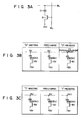
- Fig. 3A shows an equivalent circuit of the memory cell.
- the drain region of a MOSFET Q which is the n +- type layer 12 common to all bits, as described with reference to Fig. 2, is connected to a power supply voltage Vcc (e.g., 5 V).
- Vcc e.g. 5 V
- a Vcc line is, therefore, in contact with the n +- type layer 12 in the periphery of the chip.
- the gate electrode and word line WL of the MOSFET Q is formed of the first polycrystalline silicon film 22, and the second electrode and bit line BL of a MOS capacitor C is formed of the second polycrystalline silicon film 26.
- Figs. 3B and 3C show operating voltages of the memory cell in writing, precharge and reading modes.
- the power supply voltage Vcc is a positive voltage, e.g., +5 V and a substrate potential is e.g. -3 V.
- a voltage of 8 V is applied to the word line WL of the memory cell so as to turn on the MOSFETand to set the bit line BLatO V.
- a voltage of about 5 V appears at a node Ns, thereby performing the writing operation.
- a potential of the node Ns is increased to about 9 V for a precharge mode.
- a voltage of 8 V is applied to the word line WL.
- a potential of the bit line BL is ⁇ 5- 5 x (9 - 5) x Cs ⁇ /(CB + CS) [V], where CS is a capacitance of the MOS capacitor, and CB is a capacitance of the bit line BL. Therefore, a potential of the bit line BL may be compared with a reference potential by a sense amplifier.
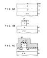
- Figs. 4Ato 4F are sectional views corresponding to that shown in Fig. 2.
- phosphorus is diffused in a high concentration in a prospective memory cell portion of a p--type Si substrate 10 after a photo engraving process (PEP) so as to form an n + -type layer 12 as a common drain region for all the memory cells.
- a p--type layer 16a containing boron in a low concentration is epitaxially grown on the resultant structure.
- An impurity concentration of the p--type layer 16a is important for determining a threshold voltage of the MOSFET, and is set at, e.g., 1 x 10 17 /cm 3 .
- n + -type layer 18a in which arsenic is diffused in a high concentration is formed on the prospective memory cell portions by the PEP.
- a mask is formed on a resultant structure or a wafer comprising such a pnpn structure by PEP. Using this mask, the wafer except for prospective MOSFET regions is selectively etched to a depth of the n + -type layer 12, thereby forming projections 14 having a predetermined periodical arrangement, as shown in Fig. 4B.
- the n + -type layer 18 remaining on each projection 14 serves as a source region of the MOSFET and a first electrode of the MOS capacitor for each memory cell, and the p--type layer 16 serves as a channel region. Thereafter, as shown in Fig.
- a thermal oxide film 20a to be a gate insulating film 20 of the MOSFETs is formed on the resultant structure, and a first polycrystalline silicon film 22a is epitaxially grown thereon.
- the gate insulating film 20 need not be thinly formed because of a sufficient channel width of the MOSFET. Therefore, a thickness of the film 20 is, e.g., 50 nm (500 ⁇ ).
- the first polycrystalline silicon film 22a is processed so as to form gate electrodes and word lines 22 which are common to the memory cells aligned along the column direction.
- the gate electrodes 22 can be formed in a self-alignment manner.
- a mask 30 shown in Fig. 4D must be formed on wiring layers 22b which connect the gate electrodes of the respective memory cell regions.
- a mask having the same height as that of the projection 14 is formed on a region between the two adjacent word lines, and thereafter, the first polycrystalline silicon film 22 may be buried in a groove between the projection 14 and the mask.
- thermal oxidefilm 20a on the n + -type layer 18 is removed, and in order to obtain a desired capacitance, a thermal oxide film of, e.g., 15 nm (150 A) thickness as an insulating film 24 is formed on the resultant structure, as shown in Fig. 4E.
- a thermal oxide film of, e.g., 15 nm (150 A) thickness as an insulating film 24 is formed on the resultant structure, as shown in Fig. 4E.
- surfaces of the first polycrystalline silicon films 22 and 22b are also oxidized, and the oxidized films serve as insulating interlayers.
- a second polycrystalline silicon film is deposited on the resultant structure, and is selectively etched by the PEP so as to form second electrodes of the MOS capacitor and bit lines 26.
- the dRAM according to this embodiment has the following advantages.
- the drain region is formed by a shallow n +- type layer
- the gate electrodes and word lines are formed by the first polycrystalline silicon films
- the second electrodes and bit lines of the MOS capacitors are formed by the second polycrystalline silicon films. For this reason, a contact hole for each memory cell is not needed. Therefore, the memory cells can be highly integrated. Since the MOS capacitors are stacked on the corresponding MOSFET along the vertical direction, the memory cells can be more highly integrated.
- MOSFETs current channels of the MOSFETs are formed on the side walls of the projections 14 of the semiconductor substrate 10 along the vertical direction.
- MOS capacitors are stacked on the corresponding MOSFETs.
- each MOS capacitor is separated from the substrate 10 by a pn junction barrier for the MOSFET. Therefore, the MOS dynamic RAM of this embodiment is resistant to soft errors.
- each MOSFET utilizes all of the surrounding portion of the projection 14 as the channel region, a channel width can be enlarged, and the insulating film need not be formed so thinly. Therefore, a variation in a threshold voltage due to hot electrons can be reduced.
- the MOS dynamic RAM of this embodiment comprises a specific memory cell structure, the manufacturing method thereof does not require a sophisticated technique. Particularly, since the memory cell regions do not require contact holes, highly integrated dRAMs can be manufactured at high yield.
- a second embodiment of a MOS dynamic RAM according to the present invention will be described hereinafter with reference to Fig. 5.
- a second electrode of each MOS capacitor constituted by a second polycrystalline silicon film 26 is independently formed for each memory cell.
- the second electrodes 26 are respectively connected to AI wiring layers 32 provided along the row direction through an insulating interlayer 28.
- the AI wiring layers 32 constitute bit lines.
- contact holes between the AI wiring layers 32 and the second polycrystalline silicon films 26 are formed on the respective memory cells, an additional element area is not required. Therefore, integration and reliability of the MOS dynamic RAM is not reduced. Since the other structures are the same as those of the first embodiment, the same reference numerals denote the same parts and a detailed description thereof is omitted.
- n +- type layer 18 as a source region of each MOSFET is formed to be sufficiently thick so that not only an upper surface but also a side surface is utilized as an electrode of the MOS capacitor.
- a second electrode 26b of each MOS capacitor opposes the side surface of the n +- type layer 18 through the insulating film 24. Since the other structures are the same as those of the first embodiment, the same reference numerals denote the same parts and a detailed description thereof is omitted. With this structure, the capacity of each MOS capacitor can be increased.
- FIG. 7 and 8 A fourth embodiment of a MOS dynamic RAM according to the present invention will be described with reference to Figs. 7 and 8.
- the memory cells are formed in the projections formed on the surface of the substrate.
- memory cells can be formed in recesses.
- Figs. 7 and 8 the same reference numerals denote the same parts corresponding to the above embodiments.
- the structure shown in Figs. 7 and 8 is obtained in the following manner.
- An n +- type layer 12 as a common drain region for all bits is formed by diffusion in a p--type Si substrate 10, and a p--type layer 16 is epitaxially grown thereon.
- N +- type layers 118 for source regions of the MOSFETs are formed in memory cell regions.
- the resultant structure is selectively etched to a depth of the n +- type layer 12 so as to form recesses 34 in the respective memory cell regions.
- a first polycrystalline silicon film 122 as a gate electrode is formed on a side wall of each recess 34 through a gate insulating film 20.
- the gate electrodes 122 are aligned along the column direction so as to be used as word lines in the same manner as described above.
- the n +- type layer 118 in each projection 14 adjacent to each recess 34 is used as a first electrode of the MOS capacitor, and a second electrode and bit line constituted by a second polycrystalline silicon film 26 is formed thereon through an insulating film 24.
- hatched portions in Fig. 7 are capacitor regions.
- stripe recesses 134 are formed along the column direction, as shown in Fig. 9.
- Gate electrodes 122 are buried in the corresponding recesses 134 along the side walls thereof. Therefore, one gate electrode 122 is commonly used for a plurality of MOS transistors formed in the single projection 14.
- the gate electrodes 122 may be buried by an etchback method in which, after forming the first polycrystalline silicon film on the overall surface, a surface of the resultant structure is flattened by a photoresist and the overall surface is etched back. Since the other structures are the same as those in the fourth embodiment, the same reference numerals denote the same parts and a detailed description thereof is omitted.
- a sixth embodiment of a MOS dynamic RAM according to the present invention will be described with reference to Fig. 11.
- different gate electrodes 222a and 222b are respectively formed on both side surfaces of each stripe recess 134 along the column direction.
- N +- type layers 118a and 118b are provided for different memory cells.
- the gate electrodes 222a and 222b may be formed in a manner such that, for example, a polycrystalline silicon film is etched by an overall anisotropic etching technique in the same manner described in Figs. 4C and 40. Since the other structures are the same as those of the fifth embodiment, the same reference numerals denote the same parts and a detailed description thereof is omitted.
- the MOS dynamic RAM can be more highly integrated than those of the above embodiments.
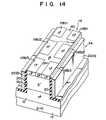
- FIG. 13 A seventh embodiment of a MOS dynamic RAM according to the present invention will be described with reference to Figs. 12 to 14.
- a wafer is used in which an n +- type layer 12 as a common drain region of MOSFETs for all memory cells is formed on a p-- type Si substrate 10, and a p--type layer 16 is epitaxially grown thereon.
- the wafer is etched by anisotropic etching such as RIE so as to form grooves which reach the n + -type layer 12, thereby forming a plurality of stripe projections 14.
- gate electrodes 222a and 222b are continuously formed on side walls of each projection 14 through a gate insulating film 20.
- the gate electrodes 222a and 222b are formed of first polycrystalline silicon films on two side surfaces of each projection 14 to serve as different word lines (e.g., WL1 and WL2, WL3 and WL4,...), as apparent from Fig. 13.
- N +- type layers 118a1, 118a2, 118a3, 118b1, 118b2 and 118b3 as respective source regions of the memory cells are dispersively formed in the upper surfaces of the corresponding projections 14 so as to be spaced apart from each other and extend along the two sides thereof.
- n +- type layers 118a1, 118a2, 118a3, 118b1, 118b2 and 118b3 as the source regions of the MOSFETs also serve as first electrodes of the MOS capacitors, and second electrodes 26 are formed thereon through a capacitor insulating film 24.
- the second electrodes 26 are formed of second polycrystalline silicon films, and constitute a plurality of bit lines BL1, BL2, BL3,... aligned along a direction perpendicular to the gate electrodes 222a and 222b.
- a region 46 indicated by a dotted line in Fig. 13 constitutes one memory cell. Hatched portions of Fig. 12 correspond to the MOS capacitor regions.
- a p +- type layer 40 for isolating the source regions of the respective memory cells is formed between said source regions in the p -type layer 16 of each projection 14.
- the p +- type layers 40 of the respective projections 14 are commonly connected to a power supply wiring layer 44 through corresponding contact holes 42 at an end face of the substrate, as shown in Fig. 12. A fixed potential is applied to the p +- type layer 40 through this power supply wiring layer 44.
- Each memory cell according to this embodiment comprises a vertical MOSFET formed on the side surface of the projection 14 and a MOS capacitor stacked thereon.
- the memory cells are formed on the two side walls of each projection 14. For this reason, a high-density and highly integrated dRAM can be obtained. Since the second electrodes 26 of the capacitors continuously formed along a single direction are used as bit lines, contact holes are not needed at the respective memory cell portions. This also facilitates high integration.
- Each MOS capacitor for accumulating data charge is separated from the substrate 10 by the n + -type layer 12 as the common drain region, thus preventing a soft error.
- the dRAM of this embodiment is resistant to soft errors.
- the p--type layers 16 as the substrate regions of the MOSFETs are separated from the substrate 10 by the n + -type layer 12, a potential thereof is fixed at -3 V by the p +- type layers 40. As a result, the p--type layers 16 do not float, and a stable transistor operation may be obtained.
- the gate electrodes 222a and 222b which serve as the word lines are arranged linearly along the side walls of the projections 14, they may be formed by RIE without forming a mask. Therefore, a manufacturing process can be simplified, resulting in increased productivity.
- a groove 50 is formed between n +- type layers 118a and 118b which are formed on both sides of the surface of each projection 14.
- a second electrode 26 is formed on an inner surface of the groove 50 through a capacitor insulating film 24.
- MOSFETs are symmetrically arranged on two side walls of each projection 14.
- MOSFETs are alternately arranged in a staggered manner. Such a structure allows a large capacity of a capacitor within a limited stripe width.
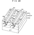
- FIG. 17 A tenth embodiment of a MOS dynamic RAM according to the present invention will be described with reference to Figs. 17 and 18.
- Fig. 17 hatched portions are MOS capacitor regions of the respective memory cells.
- memory cells are integrated on a p--type substrate 310 comprising a three-layered structure in which an n +- type layer 310b and a p--type layer 310c are sequentially formed on a p-type starting substrate 310a.
- the n +- type layer 310b is a common drain region of MOSFETs for all the memory cells.
- a p--type layer 310c is a channel region. V-shaped grooves 334 which reach the n +- type layer 310b are formed in the substrate 310.
- Gate electrodes 322 of a first polycrystalline silicon film are formed on side walls of each groove 334 through a gate insulating film 320.
- N +- type layers 318a and 318b as source regions of the MOSFETs are formed in upper portions of each projection 314.
- the n +- type layers 318a and 318b are respectively arranged to sandwich the groove 34.
- the gate electrodes 322 are commonly provided for the memory cells aligned along the column direction so as to constitute the word lines.
- Each MOS capacitor comprises a first electrode 360 of a second polycrystalline silicon film stacked on the gate electrode 322 so as to be in contact with two source regions 318a and 318b of the MOSFET for each memory cell, and a second electrode 326 of a third polycrystalline silicon film formed on the first electrode 360 through an insulating film 324.
- the second electrodes 326 are arranged along the row direction so as to constitute the bit lines.
- reference numerals 328 and 362 denote insulating interlayers.
- Figs. 19A to 19C are respectively sectional views corresponding to those of Fig. 18.
- phosphorus is diffused in the p-type starting substrate 310a to a high concentration, thereby forming the n +- type layer 310b as a common drain region for all the memory cells.
- the p--type layer 310c containing boron of a low concentration is epitaxially grown on the resultant structure.
- An impurity concentration of the p--type layer 310c is important for determining a threshold voltage of the MOSFET, and is set at, e.g., 1 x 10 17 /cm 3 .
- the substrate 310 with such a three-layered structure is etched by the PEP so as to form the V-shaped grooves 334 which reach the n +- type layer 310b.
- the V-shaped grooves 334 can be easily formed by wet etching using KOH.
- a thermal oxide film is formed on the resultant structure as the gate insulating film 320.
- the first polycrystalline silicon film is deposited on the thermal oxide film and is patterned to be buried in the V-shaped grooves 334, thereby forming the gate electrodes 322.
- the n + -type layers 318a and 318b as source regions of the respective memory cells are formed by ion-implantation.
- Fig. 20 is a perspective view showing this state.
- the V-shaped grooves 334 are continuously formed on the substrate 310 along a single direction, and the gate electrodes 332 are continuously formed in the corresponding grooves 334.
- the gate electrodes 322 also serve as word lines.
- a CVD oxide film is formed as the interlayer insulating film 362.
- Contact holes are formed in the n +- type layers 318a and 318b by the PEP, and the first electrodes 360 of the MOS capacitors are formed by the second polycrystalline silicon films.
- the first electrode 360 is formed in each memory cell so as to be in contact with the n + -type layers 318a and 318b as the source regions which sandwich the groove 334.
- a thermal oxide film of, e.g., 20 nm (200 A) is formed on the first electrodes 360 as the capacitor insulating film 324.
- the second electrodes 326 serving as the bit lines are formed by patterning.
- the dRAM according to this embodiment has the following advantages. Since vertical MOSFETs are provided in V-shaped grooves and MOS capacitors are formed thereon, the total area of the capacitor portion with respect to the total memory cell area can be large. Therefore, a large capacitance can be provided by a small memory cell area.
- the capacitor for accumulating data charge is separated from the substrate 310 by a pn junction barrier. For this reason, the memory cells are resistant to soft errors. Since each MOSFET utilizes the opposing side walls of the groove 334 as a channel region, a channel width can be widened. Therefore, the gate insulating films need not be formed so thinly, and a variation in a threshold voltage due to hot electrons can be reduced.
- the manufacturing technique of the V-shaped groove 334 is well established, and therefore, productivity can be increased.
- the dRAM of the present invention can be obtained without using an epitaxial substrate.
- the same reference numerals denote the same parts as those of the tenth embodiment, and a detailed description thereof is omitted.
- an n + -type layer 412 as a drain region of a MOSFET Q is formed by ion-implantation.
- the n +- type layer 412 is formed to be common to all the memory cells as indicated by hatched portions in Fig. 21.
- a p-type impurity is ion-implanted in the overall surface of the resultant structure so as to form a p-type layer 416 for controlling a threshold voltage of the MOSFET.
- a p-type layer 470 is also formed, at the same time, between the n +- type source regions 318a and 318b formed in the upper surface of each projection 414.
- the other structures are the same as those of the tenth embodiment.
- the step of forming an epitaxial layer can be omitted.
- An epitaxial layer has many defects. Therefore, since this embodiment does not use an epitaxial layer, it is advantageous in terms of reliability.
- the p-type layer 470 which is formed in the overall surface can be used as an element isolation layer.
- the V-shaped grooves 334 are continuously formed along one direction.
- the V-shaped grooves 334 do not have to be continuously formed, but may be formed only in the respective memory cell regions.
- n +- type layer as the drain region of the MOSFETs, is commonly formed for all the memory cell regions, it may be formed along the row or column direction in a stripe form and may be commonly connected with, e.g., an AI wiring layer in the periphery of a chip substrate.
- n +- type layer as the drain region of the MOSFETs is continuously formed along one direction and used as the bit line, and the second electrode of the capacitor is commonly provided on the overall surface and set at a fixed potential.
Landscapes
- Engineering & Computer Science (AREA)
- Manufacturing & Machinery (AREA)
- Semiconductor Memories (AREA)
Claims (31)
dadurch gekennzeichnet, daß
Applications Claiming Priority (2)
| Application Number | Priority Date | Filing Date | Title |
|---|---|---|---|
| JP190002/84 | 1984-09-11 | ||
| JP59190002A JPH0793365B2 (ja) | 1984-09-11 | 1984-09-11 | 半導体記憶装置およびその製造方法 |
Publications (3)
| Publication Number | Publication Date |
|---|---|
| EP0175433A2 EP0175433A2 (de) | 1986-03-26 |
| EP0175433A3 EP0175433A3 (en) | 1986-12-30 |
| EP0175433B1 true EP0175433B1 (de) | 1990-10-31 |
Family
ID=16250744
Family Applications (1)
| Application Number | Title | Priority Date | Filing Date |
|---|---|---|---|
| EP85302356A Expired EP0175433B1 (de) | 1984-09-11 | 1985-04-03 | Dynamisches RAM in MOS-Technologie und Verfahren zu seiner Herstellung |
Country Status (4)
| Country | Link |
|---|---|
| US (1) | US4630088A (de) |
| EP (1) | EP0175433B1 (de) |
| JP (1) | JPH0793365B2 (de) |
| DE (1) | DE3580330D1 (de) |
Families Citing this family (88)
| Publication number | Priority date | Publication date | Assignee | Title |
|---|---|---|---|---|
| US4985373A (en) * | 1982-04-23 | 1991-01-15 | At&T Bell Laboratories | Multiple insulating layer for two-level interconnected metallization in semiconductor integrated circuit structures |
| USRE33261E (en) * | 1984-07-03 | 1990-07-10 | Texas Instruments, Incorporated | Trench capacitor for high density dynamic RAM |
| US4786953A (en) * | 1984-07-16 | 1988-11-22 | Nippon Telegraph & Telephone | Vertical MOSFET and method of manufacturing the same |
| US5208657A (en) * | 1984-08-31 | 1993-05-04 | Texas Instruments Incorporated | DRAM Cell with trench capacitor and vertical channel in substrate |
| US4824793A (en) * | 1984-09-27 | 1989-04-25 | Texas Instruments Incorporated | Method of making DRAM cell with trench capacitor |
| US4914739A (en) * | 1984-10-31 | 1990-04-03 | Texas Instruments, Incorporated | Structure for contacting devices in three dimensional circuitry |
| US5102817A (en) * | 1985-03-21 | 1992-04-07 | Texas Instruments Incorporated | Vertical DRAM cell and method |
| JPH0682800B2 (ja) * | 1985-04-16 | 1994-10-19 | 株式会社東芝 | 半導体記憶装置 |
| US5164917A (en) * | 1985-06-26 | 1992-11-17 | Texas Instruments Incorporated | Vertical one-transistor DRAM with enhanced capacitance and process for fabricating |
| US5034785A (en) * | 1986-03-24 | 1991-07-23 | Siliconix Incorporated | Planar vertical channel DMOS structure |
| JPS6334955A (ja) * | 1986-07-29 | 1988-02-15 | Mitsubishi Electric Corp | 半導体装置およびその製造方法 |
| US4829017A (en) * | 1986-09-25 | 1989-05-09 | Texas Instruments Incorporated | Method for lubricating a high capacity dram cell |
| US5124764A (en) * | 1986-10-21 | 1992-06-23 | Texas Instruments Incorporated | Symmetric vertical MOS transistor with improved high voltage operation |
| JPS63114248A (ja) * | 1986-10-31 | 1988-05-19 | Texas Instr Japan Ltd | 半導体集積回路装置 |
| JPH0795568B2 (ja) * | 1987-04-27 | 1995-10-11 | 日本電気株式会社 | 半導体記憶装置 |
| US5109259A (en) * | 1987-09-22 | 1992-04-28 | Texas Instruments Incorporated | Multiple DRAM cells in a trench |
| US4949138A (en) * | 1987-10-27 | 1990-08-14 | Texas Instruments Incorporated | Semiconductor integrated circuit device |
| JPH01125858A (ja) * | 1987-11-10 | 1989-05-18 | Fujitsu Ltd | 半導体装置およびその製造方法 |
| JP2606857B2 (ja) * | 1987-12-10 | 1997-05-07 | 株式会社日立製作所 | 半導体記憶装置の製造方法 |
| JP2655859B2 (ja) * | 1988-02-03 | 1997-09-24 | 株式会社日立製作所 | 半導体記憶装置 |
| EP0333426B1 (de) * | 1988-03-15 | 1996-07-10 | Kabushiki Kaisha Toshiba | Dynamischer RAM |
| US5105245A (en) * | 1988-06-28 | 1992-04-14 | Texas Instruments Incorporated | Trench capacitor DRAM cell with diffused bit lines adjacent to a trench |
| US5225363A (en) * | 1988-06-28 | 1993-07-06 | Texas Instruments Incorporated | Trench capacitor DRAM cell and method of manufacture |
| US4958206A (en) * | 1988-06-28 | 1990-09-18 | Texas Instruments Incorporated | Diffused bit line trench capacitor dram cell |
| US4927779A (en) * | 1988-08-10 | 1990-05-22 | International Business Machines Corporation | Complementary metal-oxide-semiconductor transistor and one-capacitor dynamic-random-access memory cell and fabrication process therefor |
| US5258635A (en) * | 1988-09-06 | 1993-11-02 | Kabushiki Kaisha Toshiba | MOS-type semiconductor integrated circuit device |
| US4920065A (en) * | 1988-10-31 | 1990-04-24 | International Business Machines Corporation | Method of making ultra dense dram cells |
| US5136534A (en) * | 1989-06-30 | 1992-08-04 | Texas Instruments Incorporated | Method and apparatus for a filament channel pass gate ferroelectric capacitor memory cell |
| US5192704A (en) * | 1989-06-30 | 1993-03-09 | Texas Instruments Incorporated | Method and apparatus for a filament channel pass gate ferroelectric capacitor memory cell |
| US5276343A (en) * | 1990-04-21 | 1994-01-04 | Kabushiki Kaisha Toshiba | Semiconductor memory device having a bit line constituted by a semiconductor layer |
| JPH0775247B2 (ja) * | 1990-05-28 | 1995-08-09 | 株式会社東芝 | 半導体記憶装置 |
| US5036020A (en) * | 1990-08-31 | 1991-07-30 | Texas Instrument Incorporated | Method of fabricating microelectronic device incorporating capacitor having lowered topographical profile |
| US5073519A (en) * | 1990-10-31 | 1991-12-17 | Texas Instruments Incorporated | Method of fabricating a vertical FET device with low gate to drain overlap capacitance |
| US5087581A (en) * | 1990-10-31 | 1992-02-11 | Texas Instruments Incorporated | Method of forming vertical FET device with low gate to source overlap capacitance |
| JP2601022B2 (ja) * | 1990-11-30 | 1997-04-16 | 日本電気株式会社 | 半導体装置の製造方法 |
| KR940006679B1 (ko) * | 1991-09-26 | 1994-07-25 | 현대전자산업 주식회사 | 수직형 트랜지스터를 갖는 dram셀 및 그 제조방법 |
| US5214301A (en) * | 1991-09-30 | 1993-05-25 | Motorola, Inc. | Field effect transistor having control and current electrodes positioned at a planar elevated surface |
| US5158901A (en) * | 1991-09-30 | 1992-10-27 | Motorola, Inc. | Field effect transistor having control and current electrodes positioned at a planar elevated surface and method of formation |
| JP3405553B2 (ja) * | 1991-12-06 | 2003-05-12 | 株式会社東芝 | 半導体装置及びその製造方法 |
| JP3311070B2 (ja) * | 1993-03-15 | 2002-08-05 | 株式会社東芝 | 半導体装置 |
| DE4447730B4 (de) * | 1993-03-15 | 2006-05-18 | Kabushiki Kaisha Toshiba, Kawasaki | Halbleiteranordnung mit Grabentypelementtrennbereich und Transistorstruktur |
| JPH06268173A (ja) * | 1993-03-15 | 1994-09-22 | Toshiba Corp | 半導体記憶装置 |
| DE4327132C2 (de) * | 1993-08-12 | 1997-01-23 | Siemens Ag | Dünnfilmtransistor und Verfahren zu dessen Herstellung |
| KR0147584B1 (ko) * | 1994-03-17 | 1998-08-01 | 윤종용 | 매몰 비트라인 셀의 제조방법 |
| JP3745392B2 (ja) * | 1994-05-26 | 2006-02-15 | 株式会社ルネサステクノロジ | 半導体装置 |
| DE19519159C2 (de) * | 1995-05-24 | 1998-07-09 | Siemens Ag | DRAM-Zellenanordnung und Verfahren zu deren Herstellung |
| DE19519160C1 (de) * | 1995-05-24 | 1996-09-12 | Siemens Ag | DRAM-Zellenanordnung und Verfahren zu deren Herstellung |
| JPH0982918A (ja) | 1995-09-19 | 1997-03-28 | Toshiba Corp | 半導体記憶装置およびその製造方法 |
| US6389582B1 (en) * | 1995-12-21 | 2002-05-14 | John Valainis | Thermal driven placement |
| US5929476A (en) | 1996-06-21 | 1999-07-27 | Prall; Kirk | Semiconductor-on-insulator transistor and memory circuitry employing semiconductor-on-insulator transistors |
| DE19720193C2 (de) | 1997-05-14 | 2002-10-17 | Infineon Technologies Ag | Integrierte Schaltungsanordnung mit mindestens zwei vertikalen MOS-Transistoren und Verfahren zu deren Herstellung |
| US6337497B1 (en) * | 1997-05-16 | 2002-01-08 | International Business Machines Corporation | Common source transistor capacitor stack |
| US6150687A (en) | 1997-07-08 | 2000-11-21 | Micron Technology, Inc. | Memory cell having a vertical transistor with buried source/drain and dual gates |
| US6072209A (en) | 1997-07-08 | 2000-06-06 | Micro Technology, Inc. | Four F2 folded bit line DRAM cell structure having buried bit and word lines |
| EP0899790A3 (de) * | 1997-08-27 | 2006-02-08 | Infineon Technologies AG | DRAM-Zellanordnung und Verfahren zu deren Herstellung |
| US6528837B2 (en) * | 1997-10-06 | 2003-03-04 | Micron Technology, Inc. | Circuit and method for an open bit line memory cell with a vertical transistor and trench plate trench capacitor |
| US6066869A (en) | 1997-10-06 | 2000-05-23 | Micron Technology, Inc. | Circuit and method for a folded bit line memory cell with vertical transistor and trench capacitor |
| TW406406B (en) | 1998-01-12 | 2000-09-21 | Siemens Ag | DRAM-cells arrangement and its production method |
| US6025225A (en) | 1998-01-22 | 2000-02-15 | Micron Technology, Inc. | Circuits with a trench capacitor having micro-roughened semiconductor surfaces and methods for forming the same |
| US5963469A (en) | 1998-02-24 | 1999-10-05 | Micron Technology, Inc. | Vertical bipolar read access for low voltage memory cell |
| US6124729A (en) | 1998-02-27 | 2000-09-26 | Micron Technology, Inc. | Field programmable logic arrays with vertical transistors |
| US5991225A (en) * | 1998-02-27 | 1999-11-23 | Micron Technology, Inc. | Programmable memory address decode array with vertical transistors |
| DE19811882A1 (de) * | 1998-03-18 | 1999-09-23 | Siemens Ag | DRAM-Zellenanordnung und Verfahren zu deren Herstellung |
| EP0945901A1 (de) | 1998-03-23 | 1999-09-29 | Siemens Aktiengesellschaft | DRAM-Zellenanordnung mit vertikalen Transistoren und Verfahren zu deren Herstellung |
| DE19813169A1 (de) * | 1998-03-25 | 1999-10-07 | Siemens Ag | Halbleiterspeicher mit streifenförmiger Zellplatte |
| US5949700A (en) * | 1998-05-26 | 1999-09-07 | International Business Machines Corporation | Five square vertical dynamic random access memory cell |
| US6225158B1 (en) | 1998-05-28 | 2001-05-01 | International Business Machines Corporation | Trench storage dynamic random access memory cell with vertical transfer device |
| US6107133A (en) * | 1998-05-28 | 2000-08-22 | International Business Machines Corporation | Method for making a five square vertical DRAM cell |
| US6208164B1 (en) | 1998-08-04 | 2001-03-27 | Micron Technology, Inc. | Programmable logic array with vertical transistors |
| KR100423765B1 (ko) | 1998-09-25 | 2004-03-22 | 인피네온 테크놀로지스 아게 | 종형 트랜지스터를 포함하는 집적 회로 및 그 제조 방법 |
| DE19914490C1 (de) * | 1999-03-30 | 2000-07-06 | Siemens Ag | Speicherzellenanordnung und Verfahren zu deren Herstellung |
| TW461096B (en) | 1999-05-13 | 2001-10-21 | Hitachi Ltd | Semiconductor memory |
| US6500744B2 (en) | 1999-09-02 | 2002-12-31 | Micron Technology, Inc. | Methods of forming DRAM assemblies, transistor devices, and openings in substrates |
| US6603168B1 (en) * | 2000-04-20 | 2003-08-05 | Agere Systems Inc. | Vertical DRAM device with channel access transistor and stacked storage capacitor and associated method |
| DE10024876A1 (de) * | 2000-05-16 | 2001-11-29 | Infineon Technologies Ag | Vertikaler Transistor |
| DE10131627B4 (de) * | 2001-06-29 | 2006-08-10 | Infineon Technologies Ag | Verfahren zum Herstellen einer Halbleiterspeichereinrichtung |
| DE10362018B4 (de) * | 2003-02-14 | 2007-03-08 | Infineon Technologies Ag | Anordnung und Verfahren zur Herstellung von vertikalen Transistorzellen und transistorgesteuerten Speicherzellen |
| DE102004063025B4 (de) * | 2004-07-27 | 2010-07-29 | Hynix Semiconductor Inc., Icheon | Speicherbauelement und Verfahren zur Herstellung desselben |
| JP4898226B2 (ja) * | 2006-01-10 | 2012-03-14 | セイコーインスツル株式会社 | 縦形mosトランジスタの製造方法 |
| JP2008282459A (ja) * | 2007-05-08 | 2008-11-20 | Elpida Memory Inc | 半導体記憶装置 |
| US9443844B2 (en) | 2011-05-10 | 2016-09-13 | Semiconductor Energy Laboratory Co., Ltd. | Gain cell semiconductor memory device and driving method thereof |
| CN102760735B (zh) * | 2011-06-21 | 2015-06-17 | 钰创科技股份有限公司 | 动态记忆体结构 |
| US9190466B2 (en) * | 2013-12-27 | 2015-11-17 | International Business Machines Corporation | Independent gate vertical FinFET structure |
| WO2015125204A1 (ja) * | 2014-02-18 | 2015-08-27 | ユニサンティス エレクトロニクス シンガポール プライベート リミテッド | 半導体装置の製造方法、及び、半導体装置 |
| US9425788B1 (en) | 2015-03-18 | 2016-08-23 | Infineon Technologies Austria Ag | Current sensors and methods of improving accuracy thereof |
| KR102695150B1 (ko) * | 2016-12-09 | 2024-08-14 | 삼성전자주식회사 | 반도체 소자 및 그 제조 방법 |
| JP7454683B2 (ja) | 2021-01-28 | 2024-03-22 | チャンシン メモリー テクノロジーズ インコーポレイテッド | 半導体構造 |
| CN112908994B (zh) * | 2021-01-28 | 2023-05-26 | 长鑫存储技术有限公司 | 半导体结构 |
Family Cites Families (10)
| Publication number | Priority date | Publication date | Assignee | Title |
|---|---|---|---|---|
| US4003036A (en) * | 1975-10-23 | 1977-01-11 | American Micro-Systems, Inc. | Single IGFET memory cell with buried storage element |
| NL191683C (nl) * | 1977-02-21 | 1996-02-05 | Zaidan Hojin Handotai Kenkyu | Halfgeleidergeheugenschakeling. |
| US4353082A (en) * | 1977-07-29 | 1982-10-05 | Texas Instruments Incorporated | Buried sense line V-groove MOS random access memory |
| DE2738008A1 (de) * | 1977-08-23 | 1979-03-01 | Siemens Ag | Verfahren zum herstellen einer eintransistor-speicherzelle |
| JPS6034819B2 (ja) * | 1978-02-14 | 1985-08-10 | 工業技術院長 | 記憶装置 |
| DE2909820A1 (de) * | 1979-03-13 | 1980-09-18 | Siemens Ag | Halbleiterspeicher mit eintransistorzellen in v-mos-technologie |
| US4252579A (en) * | 1979-05-07 | 1981-02-24 | International Business Machines Corporation | Method for making single electrode U-MOSFET random access memory utilizing reactive ion etching and polycrystalline deposition |
| US4462040A (en) * | 1979-05-07 | 1984-07-24 | International Business Machines Corporation | Single electrode U-MOSFET random access memory |
| JPS5832789B2 (ja) * | 1980-07-18 | 1983-07-15 | 富士通株式会社 | 半導体メモリ |
| US4491936A (en) * | 1982-02-08 | 1985-01-01 | Mostek Corporation | Dynamic random access memory cell with increased signal margin |
-
1984
- 1984-09-11 JP JP59190002A patent/JPH0793365B2/ja not_active Expired - Fee Related
-
1985
- 1985-04-03 EP EP85302356A patent/EP0175433B1/de not_active Expired
- 1985-04-03 US US06/719,450 patent/US4630088A/en not_active Expired - Lifetime
- 1985-04-03 DE DE8585302356T patent/DE3580330D1/de not_active Expired - Lifetime
Also Published As
| Publication number | Publication date |
|---|---|
| US4630088A (en) | 1986-12-16 |
| EP0175433A2 (de) | 1986-03-26 |
| DE3580330D1 (de) | 1990-12-06 |
| JPH0793365B2 (ja) | 1995-10-09 |
| JPS6167953A (ja) | 1986-04-08 |
| EP0175433A3 (en) | 1986-12-30 |
Similar Documents
| Publication | Publication Date | Title |
|---|---|---|
| EP0175433B1 (de) | Dynamisches RAM in MOS-Technologie und Verfahren zu seiner Herstellung | |
| US4792834A (en) | Semiconductor memory device with buried layer under groove capacitor | |
| US6383860B2 (en) | Semiconductor device and method of manufacturing the same | |
| KR100675726B1 (ko) | 반도체 집적회로장치 및 그 제조방법 | |
| US4873560A (en) | Dynamic random access memory having buried word lines | |
| EP0509565B1 (de) | Halbleiterbauelement mit Bereichen unterschiedlicher Störstellenkonzentration | |
| US4855953A (en) | Semiconductor memory device having stacked memory capacitors and method for manufacturing the same | |
| US5025294A (en) | Metal insulator semiconductor type dynamic random access memory device | |
| US5100825A (en) | Method of making stacked surrounding reintrant wall capacitor | |
| US5214296A (en) | Thin-film semiconductor device and method of fabricating the same | |
| US5428236A (en) | Semiconductor memory device having trenched capicitor | |
| US5374838A (en) | Semiconductor device having different impurity concentration wells | |
| US4733374A (en) | Dynamic semiconductor memory device | |
| US4918500A (en) | Semiconductor device having trench capacitor and manufacturing method therefor | |
| EP0154685A1 (de) | Halbleiterspeichervorrichtung | |
| US5010379A (en) | Semiconductor memory device with two storage nodes | |
| US5726475A (en) | Semiconductor device having different impurity concentration wells | |
| US5917247A (en) | Static type memory cell structure with parasitic capacitor | |
| US5200353A (en) | Method of manufacturing a semiconductor device having trench capacitor | |
| JPH0642534B2 (ja) | 基板に延びている壁にコンタクトを形成する方法 | |
| JPS61140172A (ja) | 半導体記憶装置 | |
| JP2554332B2 (ja) | 1トランジスタ型ダイナミツクメモリセル | |
| JPS6240868B2 (de) | ||
| JP2760979B2 (ja) | 半導体記憶装置およびその製造方法 | |
| JP3075933B2 (ja) | 半導体記憶装置およびその製造方法 |
Legal Events
| Date | Code | Title | Description |
|---|---|---|---|
| PUAI | Public reference made under article 153(3) epc to a published international application that has entered the european phase |
Free format text: ORIGINAL CODE: 0009012 |
|
| 17P | Request for examination filed |
Effective date: 19850422 |
|
| AK | Designated contracting states |
Kind code of ref document: A2 Designated state(s): DE FR GB |
|
| PUAL | Search report despatched |
Free format text: ORIGINAL CODE: 0009013 |
|
| AK | Designated contracting states |
Kind code of ref document: A3 Designated state(s): DE FR GB |
|
| 17Q | First examination report despatched |
Effective date: 19890220 |
|
| GRAA | (expected) grant |
Free format text: ORIGINAL CODE: 0009210 |
|
| AK | Designated contracting states |
Kind code of ref document: B1 Designated state(s): DE FR GB |
|
| PG25 | Lapsed in a contracting state [announced via postgrant information from national office to epo] |
Ref country code: FR Effective date: 19901031 |
|
| REF | Corresponds to: |
Ref document number: 3580330 Country of ref document: DE Date of ref document: 19901206 |
|
| EN | Fr: translation not filed | ||
| PG25 | Lapsed in a contracting state [announced via postgrant information from national office to epo] |
Ref country code: GB Effective date: 19910403 |
|
| PLBE | No opposition filed within time limit |
Free format text: ORIGINAL CODE: 0009261 |
|
| STAA | Information on the status of an ep patent application or granted ep patent |
Free format text: STATUS: NO OPPOSITION FILED WITHIN TIME LIMIT |
|
| 26N | No opposition filed | ||
| GBPC | Gb: european patent ceased through non-payment of renewal fee | ||
| PGFP | Annual fee paid to national office [announced via postgrant information from national office to epo] |
Ref country code: DE Payment date: 20040415 Year of fee payment: 20 |