EP0176771A2 - Transistor bipolaire de puissance à tension de claquage variable - Google Patents
Transistor bipolaire de puissance à tension de claquage variable Download PDFInfo
- Publication number
- EP0176771A2 EP0176771A2 EP85110888A EP85110888A EP0176771A2 EP 0176771 A2 EP0176771 A2 EP 0176771A2 EP 85110888 A EP85110888 A EP 85110888A EP 85110888 A EP85110888 A EP 85110888A EP 0176771 A2 EP0176771 A2 EP 0176771A2
- Authority
- EP
- European Patent Office
- Prior art keywords
- emitter
- base
- contact
- power transistor
- zone
- Prior art date
- Legal status (The legal status is an assumption and is not a legal conclusion. Google has not performed a legal analysis and makes no representation as to the accuracy of the status listed.)
- Withdrawn
Links
Images
Classifications
-
- H—ELECTRICITY
- H10—SEMICONDUCTOR DEVICES; ELECTRIC SOLID-STATE DEVICES NOT OTHERWISE PROVIDED FOR
- H10D—INORGANIC ELECTRIC SEMICONDUCTOR DEVICES
- H10D84/00—Integrated devices formed in or on semiconductor substrates that comprise only semiconducting layers, e.g. on Si wafers or on GaAs-on-Si wafers
- H10D84/101—Integrated devices comprising main components and built-in components, e.g. IGBT having built-in freewheel diode
- H10D84/121—BJTs having built-in components
Definitions
- the invention relates to a bipolar power transistor with a circuit part lying parallel to the base-emitter path for changing the breakdown voltage in the blocked state according to the preamble of claim 1.
- a power transistor of this type is known, for example, from the manual for shaft transistors from Thomson-CSF, 1979, pp. 9-11, in particular Figure 1, in addition to a collector-emitter breakdown voltage U cE0 with an open base, that is to say without connecting a resistor in parallel to the base-emitter path, it has an increased breakdown voltage U CER when such a resistor is connected.
- the disadvantage here is that the circuit part mentioned contains an external resistor and an electronic switch that can be switched on if required, which considerably increases the circuit complexity.
- the invention has for its object to provide a bipolar power transistor of the type mentioned, which despite a much simpler construction than the one described above in the blocked state from a first collector-emitter breakdown voltage U CEO ' which is present on an unwired base, to a higher one Collector-emitter breakdown voltage is switchable. This is achieved according to the invention by training according to the characterizing part of patent claim 1
- the advantage that can be achieved with the invention is, in particular, that the blocking capability of the power transistor is improved without great circuitry outlay by driving a monolithically integrated field effect transistor, the switching on of the field effect transistor leading to an increase in the collector-emitter breakdown voltage.
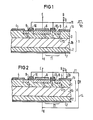
- FIG. 1 shows part of a disk-shaped body 1 made of doped semiconductor material, for example silicon, which has a first partial layer 1 with a doping concentration of, for example, 10 14 cm
- second partial layer 2 with a doping concentration of, for example, 10 17 cm
- the base of this transistor consists of a p-type zone 3 inserted in 1 with a doping concentration of, for example, 10 16 cm, which extends to the interface 1 a and in this with a base con clock 4 is provided, which is connected to a base connection B.
- An n-type emitter region 5 is inserted into zone 3 and is connected to an emitter terminal E via an emitter contact 6 located in interface 1.
- the second sub-layer 2 is provided with a collector contact 7, which is connected to a collector connection K.
- T1 represents an emitter-base short-circuit structure that can be controlled via 11.
- an inversion channel 12 is formed in the part of zone 3 adjacent to 1 a below the gate electrode 10, which part 5 and 8 and thus the connections E and B with low resistance to each other or short-circuits.
- the control input 11 is de-energized, the inversion channel 12 is not present, so that the short circuit is ineffective.
- a load current flows between K and E as a function of a base current I B fed in via B in the direction of the arrow.
- a collector voltage source in an external load circuit which biases K against E in a positive manner.
- Base current l B switched off.
- the blocking capability of the power transistor is therefore limited to collector-emitter voltages below the breakdown voltage. Without the effective switching of the short-circuit path between E and B running through the inversion channel 12, the collector-emitter breakdown voltage corresponds to a value U CEO ' which applies to an open, that is to say unshaded base connection B.
- a positive control voltage now becomes in the blocked state of the power transistor + U, applied to the control input 11 in order to raise the breakdown voltage from the above-mentioned value U CEO to a substantially higher value U CEK , which is valid for the short circuit path between E and B which is activated.
- FIG. 2 shown. It differs from Fig. 1 only in that the control input 11 with the grafan circuit K is connected via a line 14.
- the other circuit parts correspond to FIG. 1 and are provided with the same reference numerals as there. 2 has a collector-emitter breakdown voltage which, depending on the collector voltage supplied via K, is automatically raised from a value U CEO to the value U CEK when the collector voltage exceeds the threshold voltage value of T1 .
- This threshold voltage can be determined by a corresponding doping concentration of the part of zone 3 and 5 lying between 5 and 8
- the threshold voltage is set to a desired value by the thickness of the gate insulation layer 9. It applies here that the threshold voltage also increases with increasing doping concentration and thickness of the gate insulation layer
- a Zener diode ZD is advantageously connected in FIG. 2 between the control input 11 and the base connection B or the base contact 4 and a current limiting resistor R is inserted into the line 14.
- R and ZD cause a voltage division of the reverse voltage applied to K and thereby prevent the partial voltage applied to the gate insulation layer 9 from exceeding the control voltage of ZD, so that the layer 9 cannot be loaded beyond the breakdown field strength.
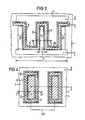
- FIG. 3 shows a top view of a preferred embodiment of the power transistor according to FIG. 1.
- the emitter region here consists of a plurality of strip-shaped partial regions 5 ', 5 "and 5"' running in the vertical direction.
- the emitter contact 6 ' has a comb-shaped lateral boundary with three finger-like projections pointing upwards, which contact these partial areas, and with a lower, horizontally extending web. 1 is to be understood as a sectional illustration along the line I - from FIG. 3.
- the source region 8 extends in a meandering manner along the upper boundary of 6.
- the gate electrode 10 also has such a meandering course.
- the base contact 4 is in turn shaped like a comb and, with two finger-like attachments pointing downward, projects into the spaces between the upward attachments of the emitter contact 6. This configuration can be referred to as a fingering of the emitter and base contacts 6, 4.
- FIG. 4 shows a top view of another preferred embodiment of the power transistor according to FIG. 1.
- the emitter region 5 has a rectangular or strip-shaped lateral boundary.
- the source region 8, the gate electrode 10 and the emitter contact 6 also have rectangular boundaries.
- the base contact 4 is provided with a rectangular recess 15 so that it slightly overlaps the outer edge of the source region 8.
- Fig. 1 is to be understood as a sectional view along the line I '- 1' of Fig. 4.
- a second, similarly formed, island-shaped emitter structure is arranged according to FIG. 4 next to the one described above.
- the connections E and 11 are connected to the corresponding parts 6 and 10 of both structures.
- the base contact 4 surrounds both emitter structures and has a recess for each of them.
- a large number of comb-like emitter contacts 6 and emitter regions 5 'to 5 "' which are designed according to FIG. 3 and fingered with corresponding base structures, or a large number of island-shaped emitter structures according to FIG. 4 over the interface 1 of the semiconductor body 1
- the parts 4, 6 and 10 of these structures are each connected to common connections E, B and 11 of the power transistor, in which case an emitter sub-region 5 'according to Fig. 3 can have a width b of 50 ⁇ m and a length of about 1 mm, for example The length of a comb-like emitter contact structure 6, which is indicated by 1 in Fig.
- Zone 3 can be 5 mm, for example, and the depth of penetration of an emitter region 5 or 5 'into zone 3 is expediently 0.3 to 2 ⁇ m Zone 3 can be approximately 3 to 5 ⁇ m, while the thickness of partial layer 1 b is selected, for example, to 10 to 50 ⁇ m.
- the sub-layers 1 b and 2 can also be replaced by a uniformly doped, n-conducting layer.
Landscapes
- Bipolar Transistors (AREA)
Applications Claiming Priority (2)
| Application Number | Priority Date | Filing Date | Title |
|---|---|---|---|
| DE3435716 | 1984-09-28 | ||
| DE3435716 | 1984-09-28 |
Publications (2)
| Publication Number | Publication Date |
|---|---|
| EP0176771A2 true EP0176771A2 (fr) | 1986-04-09 |
| EP0176771A3 EP0176771A3 (fr) | 1988-01-13 |
Family
ID=6246662
Family Applications (1)
| Application Number | Title | Priority Date | Filing Date |
|---|---|---|---|
| EP85110888A Withdrawn EP0176771A3 (fr) | 1984-09-28 | 1985-08-29 | Transistor bipolaire de puissance à tension de claquage variable |
Country Status (2)
| Country | Link |
|---|---|
| EP (1) | EP0176771A3 (fr) |
| JP (1) | JPS6185866A (fr) |
Cited By (3)
| Publication number | Priority date | Publication date | Assignee | Title |
|---|---|---|---|---|
| EP0180003A3 (fr) * | 1984-09-28 | 1988-01-13 | Siemens Aktiengesellschaft | Transistor bipolaire de puissance |
| EP0337629A1 (fr) * | 1988-04-14 | 1989-10-18 | Powerex, Inc. | Commutateur à gain variable |
| WO2003069362A1 (fr) * | 2002-02-12 | 2003-08-21 | Infineon Technologies Ag | Procede et dispositif pour detecter un claquage d'un transistor bipolaire |
Families Citing this family (1)
| Publication number | Priority date | Publication date | Assignee | Title |
|---|---|---|---|---|
| EP0860883B1 (fr) * | 1996-09-06 | 2008-11-12 | Mitsubishi Denki Kabushiki Kaisha | Transistor et son procede de fabrication |
Family Cites Families (5)
| Publication number | Priority date | Publication date | Assignee | Title |
|---|---|---|---|---|
| NL293292A (fr) * | 1962-06-11 | |||
| US3271640A (en) * | 1962-10-11 | 1966-09-06 | Fairchild Camera Instr Co | Semiconductor tetrode |
| BE788874A (fr) * | 1971-09-17 | 1973-01-02 | Western Electric Co | Module de circuit integre |
| JPS6174362A (ja) * | 1984-09-19 | 1986-04-16 | Hitachi Ltd | 半導体装置 |
| EP0180003A3 (fr) * | 1984-09-28 | 1988-01-13 | Siemens Aktiengesellschaft | Transistor bipolaire de puissance |
-
1985
- 1985-08-29 EP EP85110888A patent/EP0176771A3/fr not_active Withdrawn
- 1985-09-26 JP JP60213610A patent/JPS6185866A/ja active Pending
Cited By (4)
| Publication number | Priority date | Publication date | Assignee | Title |
|---|---|---|---|---|
| EP0180003A3 (fr) * | 1984-09-28 | 1988-01-13 | Siemens Aktiengesellschaft | Transistor bipolaire de puissance |
| EP0337629A1 (fr) * | 1988-04-14 | 1989-10-18 | Powerex, Inc. | Commutateur à gain variable |
| US5128742A (en) * | 1988-04-14 | 1992-07-07 | Powerex, Inc. | Variable gain switch |
| WO2003069362A1 (fr) * | 2002-02-12 | 2003-08-21 | Infineon Technologies Ag | Procede et dispositif pour detecter un claquage d'un transistor bipolaire |
Also Published As
| Publication number | Publication date |
|---|---|
| JPS6185866A (ja) | 1986-05-01 |
| EP0176771A3 (fr) | 1988-01-13 |
Similar Documents
| Publication | Publication Date | Title |
|---|---|---|
| DE102014110366B4 (de) | Mos-leistungstransistor mit integriertem gatewiderstand | |
| DE19903028B4 (de) | MOS-Halbleiteranordnung | |
| EP0886883B1 (fr) | Dispositifs electroniques pour la commutation de courants electriques, pour des tensions de blocage elevees et avec de faibles pertes d'energie a l'etat conduct | |
| DE69414311T2 (de) | Halbleiteranordnung mit einer Bipolarfeldeffektanordnung mit isoliertem Gate | |
| DE19704995B4 (de) | Integrierte Hochspannungs-Leistungsschaltung | |
| DE19811297B4 (de) | MOS-Halbleitervorrichtung mit hoher Durchbruchspannung | |
| EP0118785B1 (fr) | Protection bipolaire contre les surintensités | |
| DE69428894T2 (de) | Bipolartransistor mit isolierter Steuerelektrode | |
| DE19914697B4 (de) | Verarmungs-MOS-Halbleiterbauelement und MOS-Leistungs-IC | |
| DE3689782T2 (de) | Anordnung mit isoliertem Gate. | |
| DE19523172A1 (de) | Bidirektionaler Thyristor | |
| DE19526537A1 (de) | Thyristor | |
| DE2047166B2 (de) | Integrierte Halbleiteranordnung | |
| DE69302244T2 (de) | Halbleiter-Schutzkomponente | |
| DE69320033T2 (de) | Monolitisch integrierte Struktur eines vertikalen Bipolar- und eines vertikalen MOSFET-Transistors | |
| DE1489894B2 (de) | In zwei richtungen schaltbares halbleiterbauelement | |
| DE69325994T2 (de) | Integrierte Struktur eines Strom-Fühlwiderstandes für Leistungs-MOSFET-Vorrichtungen, insbesondere für Leistungs-MOSFET-Vorrichtungen mit einer Überstrom-Selbst-Schutzschaltung | |
| DE69930715T2 (de) | Elektronische Halbleiterleistung mit integrierter Diode | |
| DE69421119T2 (de) | Thyristor mit isolierten Gate und Methode, derselben zu Betreiben | |
| EP1284019B1 (fr) | Composant semi-conducteur de puissance | |
| DE2531249A1 (de) | Vielschicht-thyristor | |
| EP0017980B1 (fr) | Thyristor contrôlé par un transistor à effet de champ | |
| EP0176771A2 (fr) | Transistor bipolaire de puissance à tension de claquage variable | |
| WO2000033380A1 (fr) | Element a semiconducteur pouvant etre commande, comprenant une resistance de grille en serie | |
| EP1259989B1 (fr) | Composant semi-conducteur integre de facon monolithique |
Legal Events
| Date | Code | Title | Description |
|---|---|---|---|
| PUAI | Public reference made under article 153(3) epc to a published international application that has entered the european phase |
Free format text: ORIGINAL CODE: 0009012 |
|
| 17P | Request for examination filed |
Effective date: 19850905 |
|
| AK | Designated contracting states |
Kind code of ref document: A2 Designated state(s): DE FR GB IT SE |
|
| PUAL | Search report despatched |
Free format text: ORIGINAL CODE: 0009013 |
|
| AK | Designated contracting states |
Kind code of ref document: A3 Designated state(s): DE FR GB IT SE |
|
| STAA | Information on the status of an ep patent application or granted ep patent |
Free format text: STATUS: THE APPLICATION IS DEEMED TO BE WITHDRAWN |
|
| 18D | Application deemed to be withdrawn |
Effective date: 19890301 |
|
| RIN1 | Information on inventor provided before grant (corrected) |
Inventor name: STOISIEK, MICHAEL, DR. DIPL.-PHYS. |