EP0178447A2 - Une méthode de fabrication d'un circuit intégré basé sur la technologie semi-conducteur sur isolant - Google Patents
Une méthode de fabrication d'un circuit intégré basé sur la technologie semi-conducteur sur isolant Download PDFInfo
- Publication number
- EP0178447A2 EP0178447A2 EP85111301A EP85111301A EP0178447A2 EP 0178447 A2 EP0178447 A2 EP 0178447A2 EP 85111301 A EP85111301 A EP 85111301A EP 85111301 A EP85111301 A EP 85111301A EP 0178447 A2 EP0178447 A2 EP 0178447A2
- Authority
- EP
- European Patent Office
- Prior art keywords
- layer
- semiconductor
- semiconductor device
- fabrication method
- set forth
- Prior art date
- Legal status (The legal status is an assumption and is not a legal conclusion. Google has not performed a legal analysis and makes no representation as to the accuracy of the status listed.)
- Granted
Links
Images



Classifications
-
- H—ELECTRICITY
- H10—SEMICONDUCTOR DEVICES; ELECTRIC SOLID-STATE DEVICES NOT OTHERWISE PROVIDED FOR
- H10D—INORGANIC ELECTRIC SEMICONDUCTOR DEVICES
- H10D84/00—Integrated devices formed in or on semiconductor substrates that comprise only semiconducting layers, e.g. on Si wafers or on GaAs-on-Si wafers
- H10D84/01—Manufacture or treatment
- H10D84/02—Manufacture or treatment characterised by using material-based technologies
- H10D84/03—Manufacture or treatment characterised by using material-based technologies using Group IV technology, e.g. silicon technology or silicon-carbide [SiC] technology
- H10D84/038—Manufacture or treatment characterised by using material-based technologies using Group IV technology, e.g. silicon technology or silicon-carbide [SiC] technology using silicon technology, e.g. SiGe
-
- H—ELECTRICITY
- H10—SEMICONDUCTOR DEVICES; ELECTRIC SOLID-STATE DEVICES NOT OTHERWISE PROVIDED FOR
- H10D—INORGANIC ELECTRIC SEMICONDUCTOR DEVICES
- H10D84/00—Integrated devices formed in or on semiconductor substrates that comprise only semiconducting layers, e.g. on Si wafers or on GaAs-on-Si wafers
-
- H—ELECTRICITY
- H10—SEMICONDUCTOR DEVICES; ELECTRIC SOLID-STATE DEVICES NOT OTHERWISE PROVIDED FOR
- H10D—INORGANIC ELECTRIC SEMICONDUCTOR DEVICES
- H10D30/00—Field-effect transistors [FET]
- H10D30/60—Insulated-gate field-effect transistors [IGFET]
- H10D30/67—Thin-film transistors [TFT]
- H10D30/674—Thin-film transistors [TFT] characterised by the active materials
- H10D30/6741—Group IV materials, e.g. germanium or silicon carbide
- H10D30/6743—Silicon
- H10D30/6744—Monocrystalline silicon
-
- H—ELECTRICITY
- H10—SEMICONDUCTOR DEVICES; ELECTRIC SOLID-STATE DEVICES NOT OTHERWISE PROVIDED FOR
- H10D—INORGANIC ELECTRIC SEMICONDUCTOR DEVICES
- H10D84/00—Integrated devices formed in or on semiconductor substrates that comprise only semiconducting layers, e.g. on Si wafers or on GaAs-on-Si wafers
- H10D84/01—Manufacture or treatment
- H10D84/0123—Integrating together multiple components covered by H10D12/00 or H10D30/00, e.g. integrating multiple IGBTs
- H10D84/0126—Integrating together multiple components covered by H10D12/00 or H10D30/00, e.g. integrating multiple IGBTs the components including insulated gates, e.g. IGFETs
-
- H—ELECTRICITY
- H10—SEMICONDUCTOR DEVICES; ELECTRIC SOLID-STATE DEVICES NOT OTHERWISE PROVIDED FOR
- H10D—INORGANIC ELECTRIC SEMICONDUCTOR DEVICES
- H10D88/00—Three-dimensional [3D] integrated devices
- H10D88/01—Manufacture or treatment
-
- H—ELECTRICITY
- H10—SEMICONDUCTOR DEVICES; ELECTRIC SOLID-STATE DEVICES NOT OTHERWISE PROVIDED FOR
- H10P—GENERIC PROCESSES OR APPARATUS FOR THE MANUFACTURE OR TREATMENT OF DEVICES COVERED BY CLASS H10
- H10P14/00—Formation of materials, e.g. in the shape of layers or pillars
- H10P14/20—Formation of materials, e.g. in the shape of layers or pillars of semiconductor materials
- H10P14/24—Formation of materials, e.g. in the shape of layers or pillars of semiconductor materials using chemical vapour deposition [CVD]
-
- H—ELECTRICITY
- H10—SEMICONDUCTOR DEVICES; ELECTRIC SOLID-STATE DEVICES NOT OTHERWISE PROVIDED FOR
- H10P—GENERIC PROCESSES OR APPARATUS FOR THE MANUFACTURE OR TREATMENT OF DEVICES COVERED BY CLASS H10
- H10P14/00—Formation of materials, e.g. in the shape of layers or pillars
- H10P14/20—Formation of materials, e.g. in the shape of layers or pillars of semiconductor materials
- H10P14/38—Formation of materials, e.g. in the shape of layers or pillars of semiconductor materials characterised by treatments done after the formation of the materials
- H10P14/3802—Crystallisation or recrystallisation of non-monocrystalline semiconductor materials, e.g. regrowth
-
- H—ELECTRICITY
- H10—SEMICONDUCTOR DEVICES; ELECTRIC SOLID-STATE DEVICES NOT OTHERWISE PROVIDED FOR
- H10P—GENERIC PROCESSES OR APPARATUS FOR THE MANUFACTURE OR TREATMENT OF DEVICES COVERED BY CLASS H10
- H10P32/00—Diffusion of dopants within, into or out of wafers, substrates or parts of devices
- H10P32/30—Diffusion for doping of conductive or resistive layers
- H10P32/302—Doping polycrystalline silicon or amorphous silicon layers
-
- H—ELECTRICITY
- H10—SEMICONDUCTOR DEVICES; ELECTRIC SOLID-STATE DEVICES NOT OTHERWISE PROVIDED FOR
- H10P—GENERIC PROCESSES OR APPARATUS FOR THE MANUFACTURE OR TREATMENT OF DEVICES COVERED BY CLASS H10
- H10P34/00—Irradiation with electromagnetic or particle radiation of wafers, substrates or parts of devices
- H10P34/40—Irradiation with electromagnetic or particle radiation of wafers, substrates or parts of devices with high-energy radiation
- H10P34/42—Irradiation with electromagnetic or particle radiation of wafers, substrates or parts of devices with high-energy radiation with electromagnetic radiation, e.g. laser annealing
-
- H—ELECTRICITY
- H10—SEMICONDUCTOR DEVICES; ELECTRIC SOLID-STATE DEVICES NOT OTHERWISE PROVIDED FOR
- H10P—GENERIC PROCESSES OR APPARATUS FOR THE MANUFACTURE OR TREATMENT OF DEVICES COVERED BY CLASS H10
- H10P90/00—Preparation of wafers not covered by a single main group of this subclass, e.g. wafer reinforcement
- H10P90/19—Preparing inhomogeneous wafers
- H10P90/1904—Preparing vertically inhomogeneous wafers
- H10P90/1906—Preparing SOI wafers
-
- H—ELECTRICITY
- H10—SEMICONDUCTOR DEVICES; ELECTRIC SOLID-STATE DEVICES NOT OTHERWISE PROVIDED FOR
- H10W—GENERIC PACKAGES, INTERCONNECTIONS, CONNECTORS OR OTHER CONSTRUCTIONAL DETAILS OF DEVICES COVERED BY CLASS H10
- H10W10/00—Isolation regions in semiconductor bodies between components of integrated devices
- H10W10/01—Manufacture or treatment
- H10W10/061—Manufacture or treatment using SOI processes together with lateral isolation, e.g. combinations of SOI and shallow trench isolations
-
- H—ELECTRICITY
- H10—SEMICONDUCTOR DEVICES; ELECTRIC SOLID-STATE DEVICES NOT OTHERWISE PROVIDED FOR
- H10W—GENERIC PACKAGES, INTERCONNECTIONS, CONNECTORS OR OTHER CONSTRUCTIONAL DETAILS OF DEVICES COVERED BY CLASS H10
- H10W10/00—Isolation regions in semiconductor bodies between components of integrated devices
- H10W10/10—Isolation regions comprising dielectric materials
- H10W10/181—Semiconductor-on-insulator [SOI] isolation regions, e.g. buried oxide regions of SOI wafers
-
- H—ELECTRICITY
- H10—SEMICONDUCTOR DEVICES; ELECTRIC SOLID-STATE DEVICES NOT OTHERWISE PROVIDED FOR
- H10W—GENERIC PACKAGES, INTERCONNECTIONS, CONNECTORS OR OTHER CONSTRUCTIONAL DETAILS OF DEVICES COVERED BY CLASS H10
- H10W10/00—Isolation regions in semiconductor bodies between components of integrated devices
- H10W10/01—Manufacture or treatment
- H10W10/011—Manufacture or treatment of isolation regions comprising dielectric materials
- H10W10/014—Manufacture or treatment of isolation regions comprising dielectric materials using trench refilling with dielectric materials, e.g. shallow trench isolations
-
- H—ELECTRICITY
- H10—SEMICONDUCTOR DEVICES; ELECTRIC SOLID-STATE DEVICES NOT OTHERWISE PROVIDED FOR
- H10W—GENERIC PACKAGES, INTERCONNECTIONS, CONNECTORS OR OTHER CONSTRUCTIONAL DETAILS OF DEVICES COVERED BY CLASS H10
- H10W10/00—Isolation regions in semiconductor bodies between components of integrated devices
- H10W10/10—Isolation regions comprising dielectric materials
- H10W10/17—Isolation regions comprising dielectric materials formed using trench refilling with dielectric materials, e.g. shallow trench isolations
-
- Y—GENERAL TAGGING OF NEW TECHNOLOGICAL DEVELOPMENTS; GENERAL TAGGING OF CROSS-SECTIONAL TECHNOLOGIES SPANNING OVER SEVERAL SECTIONS OF THE IPC; TECHNICAL SUBJECTS COVERED BY FORMER USPC CROSS-REFERENCE ART COLLECTIONS [XRACs] AND DIGESTS
- Y10—TECHNICAL SUBJECTS COVERED BY FORMER USPC
- Y10S—TECHNICAL SUBJECTS COVERED BY FORMER USPC CROSS-REFERENCE ART COLLECTIONS [XRACs] AND DIGESTS
- Y10S148/00—Metal treatment
- Y10S148/09—Laser anneal
-
- Y—GENERAL TAGGING OF NEW TECHNOLOGICAL DEVELOPMENTS; GENERAL TAGGING OF CROSS-SECTIONAL TECHNOLOGIES SPANNING OVER SEVERAL SECTIONS OF THE IPC; TECHNICAL SUBJECTS COVERED BY FORMER USPC CROSS-REFERENCE ART COLLECTIONS [XRACs] AND DIGESTS
- Y10—TECHNICAL SUBJECTS COVERED BY FORMER USPC
- Y10S—TECHNICAL SUBJECTS COVERED BY FORMER USPC CROSS-REFERENCE ART COLLECTIONS [XRACs] AND DIGESTS
- Y10S148/00—Metal treatment
- Y10S148/091—Laser beam processing of fets
Definitions
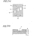
- the present invention relates to a semiconductor device based on so-called SOI (semiconductor on insulator) technology, particularly to a method for fabricating the semiconductor device by using an anti-reflecting film for laser beam irradiation.
- SOI semiconductor on insulator
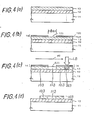
- references 103 and 203 designate a domain recrystallized into a polycrystalline state and that in molten state, respectively.
- An insulating coating layer 19 is formed on each of the transistor structure.
- the insulating coating layer 19 having thickness of about 8000 A is, then, provided with contact holes 100 through which connections to the source or drain regions 17 and 18 are provided by the respective wiring layers 110 and 120 of aluminum, for example, as shown in FIG.(g).
- a PSG (phospho-silicate glass) layer is used for the insulating coating layer 19, a heat process (conventionally referred to as a reflow process) at 1050°C, for example, is needed for blunting the sharp edge of the contact holes 100.
- a heat process at a temperature as high as 1050°C is necessary for the annealing of the ion-implanted source or drain regions 17 and 18 or the reflow process for the contact holes 100 in a PSG layer.
- the heat process at such high temperature tends to cause diffusion of doped impurities from the source or drain regions 17 and 18 to the single crystal region 113. If a grain boundary should exist in the single crystal region 113, the impurity diffusion along the grain boundary would be accelerated, and thus, the problems in the prior art, such as increased leak currents, non-uniform threshold voltages, source-drain breakdown failures, etc. in the devices formed in the recrystallized semiconductor layer, would occur.
- the IG-FETs for example, in a semiconductor integrated circuit based on an SOI technology can be free from the prior art problems relating to the grain boundaries, and therefore, superior characteristics and greater fabrication yield of the integrated circuit can also be provided. It is obvious that entire region of a device including the source or drain regions of an IG-FET, for example, can be fabricated in a grain-boundary-free region formed according to the present invention, since the grain-boundary-free region can be large as 10x20 square microns.
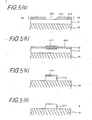
- F IGs.5(a) to 5(d) show further another embodiment of the present invention.
- a polycrystalline semiconductor layer 41, polysilicon layer, for example, having thickness of about 4000 A is formed on an insulating layer 40 having thickness of about 1 micron, and an anti-reflecting film 4 2 having an opening 421 is formed on the polysilicon layer 41, as shown in FIG.5(a).
- the anti-reflecting film 42 may has a double-layered structure comprising a Si 3 N 4 layer 422 and an underlying SiO 2 layer 423, each having a thickness 0 of about 300 A.
- the polysilicon layer 41 at the opening 421 is recrystallized to be grain boundary free by a laser beam irradiation, as described in the previous embodiments.
Landscapes
- Recrystallisation Techniques (AREA)
Applications Claiming Priority (4)
| Application Number | Priority Date | Filing Date | Title |
|---|---|---|---|
| JP59211703A JPS6189621A (ja) | 1984-10-09 | 1984-10-09 | 半導体装置の製造方法 |
| JP211703/84 | 1984-10-09 | ||
| JP60006221A JPS61166074A (ja) | 1985-01-17 | 1985-01-17 | 絶縁ゲ−ト型トランジスタ及びその製造方法 |
| JP6221/84 | 1985-01-17 |
Publications (3)
| Publication Number | Publication Date |
|---|---|
| EP0178447A2 true EP0178447A2 (fr) | 1986-04-23 |
| EP0178447A3 EP0178447A3 (en) | 1988-02-03 |
| EP0178447B1 EP0178447B1 (fr) | 1993-02-17 |
Family
ID=26340298
Family Applications (1)
| Application Number | Title | Priority Date | Filing Date |
|---|---|---|---|
| EP85111301A Expired - Lifetime EP0178447B1 (fr) | 1984-10-09 | 1985-09-06 | Une méthode de fabrication d'un circuit intégré basé sur la technologie semi-conducteur sur isolant |
Country Status (4)
| Country | Link |
|---|---|
| US (1) | US5077233A (fr) |
| EP (1) | EP0178447B1 (fr) |
| KR (1) | KR900000561B1 (fr) |
| DE (1) | DE3587100T2 (fr) |
Cited By (35)
| Publication number | Priority date | Publication date | Assignee | Title |
|---|---|---|---|---|
| EP0367446A1 (fr) * | 1988-10-20 | 1990-05-09 | Canon Kabushiki Kaisha | Commutateur semi-conducteur |
| DE4128333A1 (de) * | 1991-08-27 | 1993-03-04 | Fischer Armin | Verfahren zum gettern von soi-schichten |
| US5766989A (en) * | 1994-12-27 | 1998-06-16 | Matsushita Electric Industrial Co., Ltd. | Method for forming polycrystalline thin film and method for fabricating thin-film transistor |
| CN1039464C (zh) * | 1993-08-27 | 1998-08-05 | 株式会社半导体能源研究所 | 半导体器件及其制造方法 |
| US5811327A (en) * | 1994-03-28 | 1998-09-22 | Sharp Kabushiki Kaisha | Method and an apparatus for fabricating a semiconductor device |
| CN1041973C (zh) * | 1993-11-05 | 1999-02-03 | 株式会社半导体能源研究所 | 半导体器件 |
| US5946561A (en) * | 1991-03-18 | 1999-08-31 | Semiconductor Energy Laboratory Co., Ltd. | Semiconductor device and method for forming the same |
| US5962869A (en) * | 1988-09-28 | 1999-10-05 | Semiconductor Energy Laboratory Co., Ltd. | Semiconductor material and method for forming the same and thin film transistor |
| GB2338597A (en) * | 1998-06-09 | 1999-12-22 | Lg Lcd Inc | Method of forming a thin film transistor by laser induced crystallisation in a predetermined direction |
| GB2338598A (en) * | 1998-06-09 | 1999-12-22 | Lg Lcd Inc | Method of crystallising an amorphous silicon layer for a thin film transistor by a laser scanning technique |
| CN1051878C (zh) * | 1992-07-21 | 2000-04-26 | 株式会社半导体能源研究所 | 半导体器件及其制造方法和透明导电薄膜的制造方法 |
| CN1052110C (zh) * | 1993-02-15 | 2000-05-03 | 株式会社半导体能源研究所 | 制造半导体器件的方法 |
| CN1052572C (zh) * | 1993-12-01 | 2000-05-17 | 株式会社半导体能源研究所 | 制造半导体器件的方法 |
| CN1052571C (zh) * | 1993-06-22 | 2000-05-17 | 株式会社半导体能源研究所 | 半导体器件及其制造方法 |
| CN1052568C (zh) * | 1992-07-06 | 2000-05-17 | 株式会社半导体能源研究所 | 形成半导体器件的方法 |
| US6071764A (en) * | 1993-07-27 | 2000-06-06 | Semiconductor Energy Laboratory Co., Ltd. | Semiconductor device and process for fabricating the same |
| US6140165A (en) * | 1993-03-12 | 2000-10-31 | Semiconductor Energy Laboratory Co., Ltd. | Semiconductor device forming method |
| CN1058584C (zh) * | 1993-05-26 | 2000-11-15 | 株式会社半导体能源研究所 | 半导体器件及其制造方法 |
| US6168980B1 (en) | 1992-08-27 | 2001-01-02 | Semiconductor Energy Laboratory Co., Ltd. | Semiconductor device and method for forming the same |
| GB2354111A (en) * | 1999-07-13 | 2001-03-14 | Nec Corp | Method for forming semiconductor films at desired portions on a substrate |
| US6271066B1 (en) * | 1991-03-18 | 2001-08-07 | Semiconductor Energy Laboratory Co., Ltd. | Semiconductor material and method for forming the same and thin film transistor |
| US6300175B1 (en) | 1998-06-09 | 2001-10-09 | Lg. Philips Lcd., Co., Ltd. | Method for fabricating thin film transistor |
| US6326286B1 (en) | 1998-06-09 | 2001-12-04 | Lg. Philips Lcd Co., Ltd. | Method for crystallizing amorphous silicon layer |
| US6340830B1 (en) | 1992-06-09 | 2002-01-22 | Semiconductor Energy Laboratory Co., Ltd. | Semiconductor device and method for forming the same |
| CN1091943C (zh) * | 1992-12-04 | 2002-10-02 | 株式会社半导体能源研究所 | 制造半导体器件的方法 |
| US6521473B1 (en) | 1999-10-29 | 2003-02-18 | Lgphilips Lcd Co., Ltd. | Method of fabricating a liquid crystal display |
| US6562672B2 (en) | 1991-03-18 | 2003-05-13 | Semiconductor Energy Laboratory Co., Ltd. | Semiconductor material and method for forming the same and thin film transistor |
| US6713330B1 (en) | 1993-06-22 | 2004-03-30 | Semiconductor Energy Laboratory Co., Ltd. | Method of fabricating a thin film transistor |
| US6835586B2 (en) | 1998-12-25 | 2004-12-28 | Semiconductor Energy Laboratory Co., Ltd. | Semiconductor device and manufacturing method thereof |
| US6881615B2 (en) | 1988-09-28 | 2005-04-19 | Semiconductor Energy Laboratory Co., Ltd. | Method for crystallizing semiconductor material without exposing it to air |
| US6914302B2 (en) | 1998-12-18 | 2005-07-05 | Semiconductor Energy Laboratory Co., Ltd. | Semiconductor device and manufacturing method thereof |
| US6964890B1 (en) | 1992-03-17 | 2005-11-15 | Semiconductor Energy Laboratory Co., Ltd. | Semiconductor device and method for forming the same |
| US6997985B1 (en) | 1993-02-15 | 2006-02-14 | Semiconductor Energy Laboratory Co., Ltd. | Semiconductor, semiconductor device, and method for fabricating the same |
| US7276730B2 (en) | 1998-12-28 | 2007-10-02 | Semiconductor Energy Laboratory Co., Ltd. | Semiconductor device having a pixel matrix circuit that includes a pixel TFT and a storage capacitor |
| US8158980B2 (en) | 2001-04-19 | 2012-04-17 | Semiconductor Energy Laboratory Co., Ltd. | Semiconductor device having a pixel matrix circuit that includes a pixel TFT and a storage capacitor |
Families Citing this family (14)
| Publication number | Priority date | Publication date | Assignee | Title |
|---|---|---|---|---|
| US6875628B1 (en) | 1993-05-26 | 2005-04-05 | Semiconductor Energy Laboratory Co., Ltd. | Semiconductor device and fabrication method of the same |
| CN100472752C (zh) * | 1993-12-02 | 2009-03-25 | 株式会社半导体能源研究所 | 半导体器件的制造方法 |
| JP2900229B2 (ja) | 1994-12-27 | 1999-06-02 | 株式会社半導体エネルギー研究所 | 半導体装置およびその作製方法および電気光学装置 |
| US5985740A (en) | 1996-01-19 | 1999-11-16 | Semiconductor Energy Laboratory Co., Ltd. | Method of manufacturing a semiconductor device including reduction of a catalyst |
| JP3729955B2 (ja) | 1996-01-19 | 2005-12-21 | 株式会社半導体エネルギー研究所 | 半導体装置の作製方法 |
| US6478263B1 (en) | 1997-01-17 | 2002-11-12 | Semiconductor Energy Laboratory Co., Ltd. | Semiconductor device and its manufacturing method |
| JP3645378B2 (ja) | 1996-01-19 | 2005-05-11 | 株式会社半導体エネルギー研究所 | 半導体装置の作製方法 |
| JP3645380B2 (ja) | 1996-01-19 | 2005-05-11 | 株式会社半導体エネルギー研究所 | 半導体装置の作製方法、情報端末、ヘッドマウントディスプレイ、ナビゲーションシステム、携帯電話、ビデオカメラ、投射型表示装置 |
| US5888858A (en) | 1996-01-20 | 1999-03-30 | Semiconductor Energy Laboratory Co., Ltd. | Semiconductor device and fabrication method thereof |
| US6180439B1 (en) | 1996-01-26 | 2001-01-30 | Semiconductor Energy Laboratory Co., Ltd. | Method for fabricating a semiconductor device |
| US7056381B1 (en) | 1996-01-26 | 2006-06-06 | Semiconductor Energy Laboratory Co., Ltd. | Fabrication method of semiconductor device |
| US6100562A (en) | 1996-03-17 | 2000-08-08 | Semiconductor Energy Laboratory Co., Ltd. | Method of manufacturing a semiconductor device |
| US5956603A (en) * | 1998-08-27 | 1999-09-21 | Ultratech Stepper, Inc. | Gas immersion laser annealing method suitable for use in the fabrication of reduced-dimension integrated circuits |
| JP4101409B2 (ja) * | 1999-08-19 | 2008-06-18 | シャープ株式会社 | 半導体装置の製造方法 |
Family Cites Families (15)
| Publication number | Priority date | Publication date | Assignee | Title |
|---|---|---|---|---|
| JPS5317069A (en) * | 1976-07-30 | 1978-02-16 | Fujitsu Ltd | Semiconductor device and its production |
| JPS5548926A (en) * | 1978-10-02 | 1980-04-08 | Hitachi Ltd | Preparation of semiconductor device |
| JPS5617083A (en) * | 1979-07-20 | 1981-02-18 | Hitachi Ltd | Semiconductor device and its manufacture |
| JPS56115558A (en) * | 1980-02-18 | 1981-09-10 | Matsushita Electric Ind Co Ltd | Semiconductor integrated circuit and manufacture thereof |
| JPS577926A (en) * | 1980-06-18 | 1982-01-16 | Fujitsu Ltd | Manufacture of semiconductor device |
| US4330363A (en) * | 1980-08-28 | 1982-05-18 | Xerox Corporation | Thermal gradient control for enhanced laser induced crystallization of predefined semiconductor areas |
| JPS5799778A (en) * | 1980-12-12 | 1982-06-21 | Citizen Watch Co Ltd | Thin-film transistor |
| JPS582073A (ja) * | 1981-06-29 | 1983-01-07 | Sony Corp | 電界効果型トランジスタ |
| JPS5814524A (ja) * | 1981-07-17 | 1983-01-27 | Fujitsu Ltd | 半導体装置の製造方法 |
| JPS58115851A (ja) * | 1981-12-28 | 1983-07-09 | Seiko Epson Corp | 半導体装置の製造方法 |
| FR2535528B1 (fr) * | 1982-10-29 | 1986-01-17 | Efcis | Structure de circuit integre sur substrat isolant avec remblai isolant autour des ilots semi-conducteurs |
| JPS59228763A (ja) * | 1983-06-10 | 1984-12-22 | Seiko Epson Corp | 半導体装置 |
| JPS6089953A (ja) * | 1983-10-22 | 1985-05-20 | Agency Of Ind Science & Technol | 積層型半導体装置の製造方法 |
| JPS60150618A (ja) * | 1984-01-17 | 1985-08-08 | Mitsubishi Electric Corp | 半導体装置の製造方法 |
| US4686553A (en) * | 1985-08-02 | 1987-08-11 | General Electric Company | Low capacitance amorphous silicon field effect transistor structure |
-
1985
- 1985-09-06 DE DE8585111301T patent/DE3587100T2/de not_active Expired - Fee Related
- 1985-09-06 EP EP85111301A patent/EP0178447B1/fr not_active Expired - Lifetime
- 1985-09-27 KR KR1019850007151A patent/KR900000561B1/ko not_active Expired
-
1990
- 1990-04-23 US US07/513,045 patent/US5077233A/en not_active Expired - Fee Related
Cited By (68)
| Publication number | Priority date | Publication date | Assignee | Title |
|---|---|---|---|---|
| US7435635B2 (en) | 1988-09-28 | 2008-10-14 | Semiconductor Energy Laboratory Co., Ltd. | Method for crystallizing semiconductor material |
| US6881615B2 (en) | 1988-09-28 | 2005-04-19 | Semiconductor Energy Laboratory Co., Ltd. | Method for crystallizing semiconductor material without exposing it to air |
| US5962869A (en) * | 1988-09-28 | 1999-10-05 | Semiconductor Energy Laboratory Co., Ltd. | Semiconductor material and method for forming the same and thin film transistor |
| US5572044A (en) * | 1988-10-20 | 1996-11-05 | Canon Kabushiki Kaisha | Monocrystalline semiconductor commutator with grain boundry |
| EP0367446A1 (fr) * | 1988-10-20 | 1990-05-09 | Canon Kabushiki Kaisha | Commutateur semi-conducteur |
| US5571747A (en) * | 1988-10-20 | 1996-11-05 | Canon Kabushiki Kaisha | Method for producing a semiconductor commutator |
| US5034782A (en) * | 1988-10-20 | 1991-07-23 | Canon Kabushiki Kaisha | Semiconductor commutator with grain boundary |
| US5946561A (en) * | 1991-03-18 | 1999-08-31 | Semiconductor Energy Laboratory Co., Ltd. | Semiconductor device and method for forming the same |
| US6271066B1 (en) * | 1991-03-18 | 2001-08-07 | Semiconductor Energy Laboratory Co., Ltd. | Semiconductor material and method for forming the same and thin film transistor |
| US6562672B2 (en) | 1991-03-18 | 2003-05-13 | Semiconductor Energy Laboratory Co., Ltd. | Semiconductor material and method for forming the same and thin film transistor |
| DE4128333A1 (de) * | 1991-08-27 | 1993-03-04 | Fischer Armin | Verfahren zum gettern von soi-schichten |
| US6964890B1 (en) | 1992-03-17 | 2005-11-15 | Semiconductor Energy Laboratory Co., Ltd. | Semiconductor device and method for forming the same |
| US6340830B1 (en) | 1992-06-09 | 2002-01-22 | Semiconductor Energy Laboratory Co., Ltd. | Semiconductor device and method for forming the same |
| US6815772B2 (en) | 1992-06-09 | 2004-11-09 | Semiconductor Energy Laboratory Co., Ltd. | Dual gate MOSFET |
| US6528852B2 (en) | 1992-06-09 | 2003-03-04 | Semiconductor Energy Laboratory Co., Ltd. | Double gated electronic device and method of forming the same |
| CN1052568C (zh) * | 1992-07-06 | 2000-05-17 | 株式会社半导体能源研究所 | 形成半导体器件的方法 |
| CN1051878C (zh) * | 1992-07-21 | 2000-04-26 | 株式会社半导体能源研究所 | 半导体器件及其制造方法和透明导电薄膜的制造方法 |
| US6168980B1 (en) | 1992-08-27 | 2001-01-02 | Semiconductor Energy Laboratory Co., Ltd. | Semiconductor device and method for forming the same |
| CN1091943C (zh) * | 1992-12-04 | 2002-10-02 | 株式会社半导体能源研究所 | 制造半导体器件的方法 |
| CN1052110C (zh) * | 1993-02-15 | 2000-05-03 | 株式会社半导体能源研究所 | 制造半导体器件的方法 |
| US6997985B1 (en) | 1993-02-15 | 2006-02-14 | Semiconductor Energy Laboratory Co., Ltd. | Semiconductor, semiconductor device, and method for fabricating the same |
| US6413805B1 (en) | 1993-03-12 | 2002-07-02 | Semiconductor Energy Laboratory Co., Ltd. | Semiconductor device forming method |
| US6140165A (en) * | 1993-03-12 | 2000-10-31 | Semiconductor Energy Laboratory Co., Ltd. | Semiconductor device forming method |
| CN100350627C (zh) * | 1993-05-26 | 2007-11-21 | 株式会社半导体能源研究所 | 半导体器件 |
| CN1058584C (zh) * | 1993-05-26 | 2000-11-15 | 株式会社半导体能源研究所 | 半导体器件及其制造方法 |
| CN100379017C (zh) * | 1993-05-26 | 2008-04-02 | 株式会社半导体能源研究所 | 半导体器件 |
| US6319761B1 (en) | 1993-06-22 | 2001-11-20 | Semiconductor Energy Laboratory Co., Ltd. | Method of fabricating a thin film transistor |
| US6713330B1 (en) | 1993-06-22 | 2004-03-30 | Semiconductor Energy Laboratory Co., Ltd. | Method of fabricating a thin film transistor |
| CN1052571C (zh) * | 1993-06-22 | 2000-05-17 | 株式会社半导体能源研究所 | 半导体器件及其制造方法 |
| US6077758A (en) * | 1993-07-27 | 2000-06-20 | Semiconductor Energy Laboratory Co., Ltd. | Method of crystallizing thin films when manufacturing semiconductor devices |
| US7056775B2 (en) | 1993-07-27 | 2006-06-06 | Semiconductor Energy Laboratory Co., Ltd. | Semiconductor device and process for fabricating the same |
| US6924213B2 (en) | 1993-07-27 | 2005-08-02 | Semiconductor Energy Laboratory Co., Ltd. | Semiconductor device and process for fabricating the same |
| US6455401B1 (en) | 1993-07-27 | 2002-09-24 | Semiconductor Energy Laboratory Co., Ltd. | Methodology for producing thin film semiconductor devices by crystallizing an amorphous film with crystallization promoting material, patterning the crystallized film, and then increasing the crystallinity with an irradiation |
| US6071764A (en) * | 1993-07-27 | 2000-06-06 | Semiconductor Energy Laboratory Co., Ltd. | Semiconductor device and process for fabricating the same |
| CN1085887C (zh) * | 1993-07-27 | 2002-05-29 | 株式会社半导体能源研究所 | 制造半导体器件的方法 |
| CN1057401C (zh) * | 1993-07-27 | 2000-10-11 | 株式会社半导体能源研究所 | 半导体器件及其制造方法 |
| US7045819B2 (en) | 1993-08-27 | 2006-05-16 | Semiconductor Energy Laboratory Co., Ltd. | Semiconductor device and method for manufacturing the same |
| US6482686B1 (en) | 1993-08-27 | 2002-11-19 | Semiconductor Energy Laboratory Co., Ltd. | Method for manufacturing a semiconductor device |
| US8133770B2 (en) | 1993-08-27 | 2012-03-13 | Semiconductor Energy Laboratory Co., Ltd. | Semiconductor device and method for manufacturing the same |
| US7875508B2 (en) | 1993-08-27 | 2011-01-25 | Semiconductor Energy Laboratory Co., Ltd. | Semiconductor device and method for manufacturing the same |
| US6194254B1 (en) | 1993-08-27 | 2001-02-27 | Semiconductor Energy Laboratories Co., Ltd. | Semiconductor device and method for manufacturing the same |
| CN1039464C (zh) * | 1993-08-27 | 1998-08-05 | 株式会社半导体能源研究所 | 半导体器件及其制造方法 |
| US7410849B2 (en) | 1993-08-27 | 2008-08-12 | Semiconductor Energy Laboratory Co., Ltd. | Semiconductor device and method for manufacturing the same |
| US6475839B2 (en) | 1993-11-05 | 2002-11-05 | Semiconductor Energy Laboratory Co., Ltd. | Manufacturing of TFT device by backside laser irradiation |
| CN1041973C (zh) * | 1993-11-05 | 1999-02-03 | 株式会社半导体能源研究所 | 半导体器件 |
| US6617612B2 (en) * | 1993-11-05 | 2003-09-09 | Semiconductor Energy Laboratory Co., Ltd. | Semiconductor device and a semiconductor integrated circuit |
| US6218678B1 (en) | 1993-11-05 | 2001-04-17 | Semiconductor Energy Laboratory Co., Ltd. | Semiconductor device |
| CN1052572C (zh) * | 1993-12-01 | 2000-05-17 | 株式会社半导体能源研究所 | 制造半导体器件的方法 |
| CN1041148C (zh) * | 1994-03-28 | 1998-12-09 | 夏普公司 | 半导体装置的制造方法及所用设备 |
| US5811327A (en) * | 1994-03-28 | 1998-09-22 | Sharp Kabushiki Kaisha | Method and an apparatus for fabricating a semiconductor device |
| US5766989A (en) * | 1994-12-27 | 1998-06-16 | Matsushita Electric Industrial Co., Ltd. | Method for forming polycrystalline thin film and method for fabricating thin-film transistor |
| CN1050221C (zh) * | 1994-12-27 | 2000-03-08 | 松下电器产业株式会社 | 多结晶薄膜的形成方法和制造薄膜晶体管的方法 |
| US6177301B1 (en) | 1998-06-09 | 2001-01-23 | Lg.Philips Lcd Co., Ltd. | Method of fabricating thin film transistors for a liquid crystal display |
| US6235614B1 (en) | 1998-06-09 | 2001-05-22 | Lg. Philips Lcd Co., Ltd. | Methods of crystallizing amorphous silicon layer and fabricating thin film transistor using the same |
| GB2338597A (en) * | 1998-06-09 | 1999-12-22 | Lg Lcd Inc | Method of forming a thin film transistor by laser induced crystallisation in a predetermined direction |
| US6300175B1 (en) | 1998-06-09 | 2001-10-09 | Lg. Philips Lcd., Co., Ltd. | Method for fabricating thin film transistor |
| GB2338598B (en) * | 1998-06-09 | 2001-01-17 | Lg Lcd Inc | Methods of crystalizing amorphous silicon layer and fabricating thin film transistors using the same |
| US6326286B1 (en) | 1998-06-09 | 2001-12-04 | Lg. Philips Lcd Co., Ltd. | Method for crystallizing amorphous silicon layer |
| GB2338598A (en) * | 1998-06-09 | 1999-12-22 | Lg Lcd Inc | Method of crystallising an amorphous silicon layer for a thin film transistor by a laser scanning technique |
| GB2338597B (en) * | 1998-06-09 | 2001-01-03 | Lg Lcd Inc | Method of fabricating thin film transistors for a liquid crystal display |
| US6914302B2 (en) | 1998-12-18 | 2005-07-05 | Semiconductor Energy Laboratory Co., Ltd. | Semiconductor device and manufacturing method thereof |
| US6835586B2 (en) | 1998-12-25 | 2004-12-28 | Semiconductor Energy Laboratory Co., Ltd. | Semiconductor device and manufacturing method thereof |
| US7276730B2 (en) | 1998-12-28 | 2007-10-02 | Semiconductor Energy Laboratory Co., Ltd. | Semiconductor device having a pixel matrix circuit that includes a pixel TFT and a storage capacitor |
| US8643015B2 (en) | 1998-12-28 | 2014-02-04 | Semiconductor Energy Laboratory Co., Ltd. | Semiconductor device having a pixel matrix circuit that includes a pixel TFT and a storage capacitor |
| GB2354111A (en) * | 1999-07-13 | 2001-03-14 | Nec Corp | Method for forming semiconductor films at desired portions on a substrate |
| US6989300B1 (en) | 1999-07-13 | 2006-01-24 | Nec Corporation | Method for forming semiconductor films at desired positions on a substrate |
| US6521473B1 (en) | 1999-10-29 | 2003-02-18 | Lgphilips Lcd Co., Ltd. | Method of fabricating a liquid crystal display |
| US8158980B2 (en) | 2001-04-19 | 2012-04-17 | Semiconductor Energy Laboratory Co., Ltd. | Semiconductor device having a pixel matrix circuit that includes a pixel TFT and a storage capacitor |
Also Published As
| Publication number | Publication date |
|---|---|
| KR860003661A (ko) | 1986-05-28 |
| US5077233A (en) | 1991-12-31 |
| EP0178447A3 (en) | 1988-02-03 |
| DE3587100T2 (de) | 1993-09-09 |
| EP0178447B1 (fr) | 1993-02-17 |
| DE3587100D1 (de) | 1993-03-25 |
| KR900000561B1 (ko) | 1990-01-31 |
Similar Documents
| Publication | Publication Date | Title |
|---|---|---|
| EP0178447B1 (fr) | Une méthode de fabrication d'un circuit intégré basé sur la technologie semi-conducteur sur isolant | |
| US7056775B2 (en) | Semiconductor device and process for fabricating the same | |
| US5696386A (en) | Semiconductor device | |
| US6995432B2 (en) | Semiconductor device having a gate oxide film with some NTFTS with LDD regions and no PTFTS with LDD regions | |
| US4404735A (en) | Method for manufacturing a field isolation structure for a semiconductor device | |
| EP0145415B1 (fr) | Procédé pour la fabrication d'un dispositif semi-conducteur du type SOI | |
| US4415383A (en) | Method of fabricating semiconductor devices using laser annealing | |
| JP3586558B2 (ja) | 薄膜の改質方法及びその実施に使用する装置 | |
| JPH07335906A (ja) | 薄膜状半導体装置およびその作製方法 | |
| JPH0823105A (ja) | 表示用半導体チップの製造方法 | |
| JPH05175235A (ja) | 多結晶半導体薄膜の製造方法 | |
| US5264072A (en) | Method for recrystallizing conductive films by an indirect-heating with a thermal-conduction-controlling layer | |
| JP2009048199A (ja) | 液晶表示装置用薄膜トランジスタ基板およびその製造方法 | |
| EP0575965B1 (fr) | Procédé pour fabriquer un cristal semi-conducteur et dispositif semi-conducteur | |
| JP2002100780A (ja) | 半導体装置及びその製造方法 | |
| JPH10178178A (ja) | 半導体装置の製造方法 | |
| JPH0797565B2 (ja) | 半導体装置の製造方法 | |
| JP4695777B2 (ja) | 半導体装置の製造方法 | |
| JP2546524B2 (ja) | 薄膜トランジスタの製造方法 | |
| JPS6159820A (ja) | 半導体装置の製造方法 | |
| JP4514908B2 (ja) | 半導体装置の製造方法 | |
| JPH03148836A (ja) | 薄膜トランジスタの製造方法 | |
| JP2782027B2 (ja) | 電界効果半導体装置の作製方法 | |
| JPS6161268B2 (fr) | ||
| JP3295378B2 (ja) | 半導体装置の作製方法 |
Legal Events
| Date | Code | Title | Description |
|---|---|---|---|
| PUAI | Public reference made under article 153(3) epc to a published international application that has entered the european phase |
Free format text: ORIGINAL CODE: 0009012 |
|
| AK | Designated contracting states |
Kind code of ref document: A2 Designated state(s): DE FR GB |
|
| PUAL | Search report despatched |
Free format text: ORIGINAL CODE: 0009013 |
|
| AK | Designated contracting states |
Kind code of ref document: A3 Designated state(s): DE FR GB |
|
| 17P | Request for examination filed |
Effective date: 19880322 |
|
| 17Q | First examination report despatched |
Effective date: 19900607 |
|
| GRAA | (expected) grant |
Free format text: ORIGINAL CODE: 0009210 |
|
| AK | Designated contracting states |
Kind code of ref document: B1 Designated state(s): DE FR GB |
|
| REF | Corresponds to: |
Ref document number: 3587100 Country of ref document: DE Date of ref document: 19930325 |
|
| ET | Fr: translation filed | ||
| PGFP | Annual fee paid to national office [announced via postgrant information from national office to epo] |
Ref country code: FR Payment date: 19930929 Year of fee payment: 9 |
|
| PGFP | Annual fee paid to national office [announced via postgrant information from national office to epo] |
Ref country code: DE Payment date: 19931130 Year of fee payment: 9 |
|
| PLBE | No opposition filed within time limit |
Free format text: ORIGINAL CODE: 0009261 |
|
| STAA | Information on the status of an ep patent application or granted ep patent |
Free format text: STATUS: NO OPPOSITION FILED WITHIN TIME LIMIT |
|
| 26N | No opposition filed | ||
| PG25 | Lapsed in a contracting state [announced via postgrant information from national office to epo] |
Ref country code: FR Effective date: 19950531 |
|
| PG25 | Lapsed in a contracting state [announced via postgrant information from national office to epo] |
Ref country code: DE Effective date: 19950601 |
|
| REG | Reference to a national code |
Ref country code: FR Ref legal event code: ST |
|
| PGFP | Annual fee paid to national office [announced via postgrant information from national office to epo] |
Ref country code: GB Payment date: 19950829 Year of fee payment: 11 |
|
| PG25 | Lapsed in a contracting state [announced via postgrant information from national office to epo] |
Ref country code: GB Effective date: 19960906 |
|
| GBPC | Gb: european patent ceased through non-payment of renewal fee |
Effective date: 19960906 |