EP0367446A1 - Commutateur semi-conducteur - Google Patents
Commutateur semi-conducteur Download PDFInfo
- Publication number
- EP0367446A1 EP0367446A1 EP89310727A EP89310727A EP0367446A1 EP 0367446 A1 EP0367446 A1 EP 0367446A1 EP 89310727 A EP89310727 A EP 89310727A EP 89310727 A EP89310727 A EP 89310727A EP 0367446 A1 EP0367446 A1 EP 0367446A1
- Authority
- EP
- European Patent Office
- Prior art keywords
- conductivity type
- grain boundary
- semiconductor region
- commutator
- semiconductor
- Prior art date
- Legal status (The legal status is an assumption and is not a legal conclusion. Google has not performed a legal analysis and makes no representation as to the accuracy of the status listed.)
- Granted
Links
Images


Classifications
-
- H—ELECTRICITY
- H10—SEMICONDUCTOR DEVICES; ELECTRIC SOLID-STATE DEVICES NOT OTHERWISE PROVIDED FOR
- H10D—INORGANIC ELECTRIC SEMICONDUCTOR DEVICES
- H10D8/00—Diodes
-
- H—ELECTRICITY
- H10—SEMICONDUCTOR DEVICES; ELECTRIC SOLID-STATE DEVICES NOT OTHERWISE PROVIDED FOR
- H10D—INORGANIC ELECTRIC SEMICONDUCTOR DEVICES
- H10D62/00—Semiconductor bodies, or regions thereof, of devices having potential barriers
- H10D62/10—Shapes, relative sizes or dispositions of the regions of the semiconductor bodies; Shapes of the semiconductor bodies
- H10D62/124—Shapes, relative sizes or dispositions of the regions of semiconductor bodies or of junctions between the regions
- H10D62/126—Top-view geometrical layouts of the regions or the junctions
-
- H—ELECTRICITY
- H10—SEMICONDUCTOR DEVICES; ELECTRIC SOLID-STATE DEVICES NOT OTHERWISE PROVIDED FOR
- H10D—INORGANIC ELECTRIC SEMICONDUCTOR DEVICES
- H10D62/00—Semiconductor bodies, or regions thereof, of devices having potential barriers
- H10D62/40—Crystalline structures
-
- H—ELECTRICITY
- H10—SEMICONDUCTOR DEVICES; ELECTRIC SOLID-STATE DEVICES NOT OTHERWISE PROVIDED FOR
- H10D—INORGANIC ELECTRIC SEMICONDUCTOR DEVICES
- H10D62/00—Semiconductor bodies, or regions thereof, of devices having potential barriers
- H10D62/50—Physical imperfections
- H10D62/53—Physical imperfections the imperfections being within the semiconductor body
-
- H—ELECTRICITY
- H10—SEMICONDUCTOR DEVICES; ELECTRIC SOLID-STATE DEVICES NOT OTHERWISE PROVIDED FOR
- H10P—GENERIC PROCESSES OR APPARATUS FOR THE MANUFACTURE OR TREATMENT OF DEVICES COVERED BY CLASS H10
- H10P14/00—Formation of materials, e.g. in the shape of layers or pillars
- H10P14/20—Formation of materials, e.g. in the shape of layers or pillars of semiconductor materials
- H10P14/24—Formation of materials, e.g. in the shape of layers or pillars of semiconductor materials using chemical vapour deposition [CVD]
-
- H—ELECTRICITY
- H10—SEMICONDUCTOR DEVICES; ELECTRIC SOLID-STATE DEVICES NOT OTHERWISE PROVIDED FOR
- H10P—GENERIC PROCESSES OR APPARATUS FOR THE MANUFACTURE OR TREATMENT OF DEVICES COVERED BY CLASS H10
- H10P14/00—Formation of materials, e.g. in the shape of layers or pillars
- H10P14/20—Formation of materials, e.g. in the shape of layers or pillars of semiconductor materials
- H10P14/27—Formation of materials, e.g. in the shape of layers or pillars of semiconductor materials using selective deposition, e.g. simultaneous growth of monocrystalline and non-monocrystalline semiconductor materials
- H10P14/271—Formation of materials, e.g. in the shape of layers or pillars of semiconductor materials using selective deposition, e.g. simultaneous growth of monocrystalline and non-monocrystalline semiconductor materials characterised by the preparation of substrate for selective deposition
- H10P14/274—Formation of materials, e.g. in the shape of layers or pillars of semiconductor materials using selective deposition, e.g. simultaneous growth of monocrystalline and non-monocrystalline semiconductor materials characterised by the preparation of substrate for selective deposition using seed materials
-
- H—ELECTRICITY
- H10—SEMICONDUCTOR DEVICES; ELECTRIC SOLID-STATE DEVICES NOT OTHERWISE PROVIDED FOR
- H10P—GENERIC PROCESSES OR APPARATUS FOR THE MANUFACTURE OR TREATMENT OF DEVICES COVERED BY CLASS H10
- H10P14/00—Formation of materials, e.g. in the shape of layers or pillars
- H10P14/20—Formation of materials, e.g. in the shape of layers or pillars of semiconductor materials
- H10P14/27—Formation of materials, e.g. in the shape of layers or pillars of semiconductor materials using selective deposition, e.g. simultaneous growth of monocrystalline and non-monocrystalline semiconductor materials
- H10P14/276—Lateral overgrowth
-
- H—ELECTRICITY
- H10—SEMICONDUCTOR DEVICES; ELECTRIC SOLID-STATE DEVICES NOT OTHERWISE PROVIDED FOR
- H10P—GENERIC PROCESSES OR APPARATUS FOR THE MANUFACTURE OR TREATMENT OF DEVICES COVERED BY CLASS H10
- H10P14/00—Formation of materials, e.g. in the shape of layers or pillars
- H10P14/20—Formation of materials, e.g. in the shape of layers or pillars of semiconductor materials
- H10P14/29—Formation of materials, e.g. in the shape of layers or pillars of semiconductor materials characterised by the substrates
- H10P14/2901—Materials
- H10P14/2902—Materials being Group IVA materials
- H10P14/2905—Silicon, silicon germanium or germanium
-
- H—ELECTRICITY
- H10—SEMICONDUCTOR DEVICES; ELECTRIC SOLID-STATE DEVICES NOT OTHERWISE PROVIDED FOR
- H10P—GENERIC PROCESSES OR APPARATUS FOR THE MANUFACTURE OR TREATMENT OF DEVICES COVERED BY CLASS H10
- H10P14/00—Formation of materials, e.g. in the shape of layers or pillars
- H10P14/20—Formation of materials, e.g. in the shape of layers or pillars of semiconductor materials
- H10P14/34—Deposited materials, e.g. layers
- H10P14/3402—Deposited materials, e.g. layers characterised by the chemical composition
- H10P14/3404—Deposited materials, e.g. layers characterised by the chemical composition being Group IVA materials
- H10P14/3411—Silicon, silicon germanium or germanium
-
- Y—GENERAL TAGGING OF NEW TECHNOLOGICAL DEVELOPMENTS; GENERAL TAGGING OF CROSS-SECTIONAL TECHNOLOGIES SPANNING OVER SEVERAL SECTIONS OF THE IPC; TECHNICAL SUBJECTS COVERED BY FORMER USPC CROSS-REFERENCE ART COLLECTIONS [XRACs] AND DIGESTS
- Y10—TECHNICAL SUBJECTS COVERED BY FORMER USPC
- Y10S—TECHNICAL SUBJECTS COVERED BY FORMER USPC CROSS-REFERENCE ART COLLECTIONS [XRACs] AND DIGESTS
- Y10S438/00—Semiconductor device manufacturing: process
- Y10S438/914—Doping
- Y10S438/921—Nonselective diffusion
-
- Y—GENERAL TAGGING OF NEW TECHNOLOGICAL DEVELOPMENTS; GENERAL TAGGING OF CROSS-SECTIONAL TECHNOLOGIES SPANNING OVER SEVERAL SECTIONS OF THE IPC; TECHNICAL SUBJECTS COVERED BY FORMER USPC CROSS-REFERENCE ART COLLECTIONS [XRACs] AND DIGESTS
- Y10—TECHNICAL SUBJECTS COVERED BY FORMER USPC
- Y10S—TECHNICAL SUBJECTS COVERED BY FORMER USPC CROSS-REFERENCE ART COLLECTIONS [XRACs] AND DIGESTS
- Y10S438/00—Semiconductor device manufacturing: process
- Y10S438/914—Doping
- Y10S438/922—Diffusion along grain boundaries
Definitions
- the present invention relates to a semiconductor commutator and, more particularly, to a semiconductor commutator which is constructed by joining a semiconductor region of the first conductivity type and a semiconductor region of the second conductivity type.
- heavy metal for instance, gold is used as a recombination center for a PN diode or a PN junction diode is formed on a polycrystalline semiconductor layer and a grain boundary defect is used as a recombination center, thereby reducing the life time of the minority carriers and decreasing the delay time.
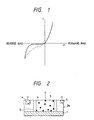
- Fig. 1 shows the current to voltage characteristics of a PN junction diode.
- a solid curve indicates the ideal preferable characteristics.
- the characteristics become as shown by a broken line.
- An object of the present invention is to provide a semiconductor commutator capable of high speed operation and an excellent current-voltage property.
- Another object of the present invention is to provide a semiconductor commutator which is constructed by joining a semiconductor region of the first conductivity type and a semiconductor region of the second conductivity type, wherein a grain boundary is provided near the junction surface of the semiconductor region of the first conductivity type and the semiconductor region of the second conductivity type so as not to cross the junction surface.
- a semiconductor commutator of the invention exhibits the good current to voltage characteristics in which the commutator can operate at a high speed and the life time of minority carriers is reduced by effectively using a grain boundary defect, as a recombination center, in which a grain boundary is arranged between a junction surface and an electrode so as not to cross the junction surface.
- Still another object of the present invention is to provide a commutator wherein a crystal forming process is executed to a substrate having a non-nucleus forming surface whose nucleus forming density is small and a free surface which has an enough small area so that only a single nucleus to be grown into single crystal is formed and on which a plurality of nucleus forming surfaces each having a nucleus forming density larger than the nucleus forming density of said non-nucleus forming surface are adjacently arranged at a predetermined distance away from one another, a monocrystal is grown from the single nucleus of each of said plurality of nucleus forming surfaces which are arranged at the predetermined distance away from one another, and the grain boundary is formed at the position where said monocrystals are joined.
- Figs. 5A to 5E are vertical sectional views showing an example of the manufacturing steps to form a crystal substrate which is used in the semiconductor commutator in the embodiment of the invention.
- Fig. 6 is a perspective view showing an Si3N4 film formed on an SiO2 film and corresponds to the manufacturing step shown in Fig. 5A.
- SiO2 film 1 having a thickness of 2000 ⁇ serving as a non-nucleus forming surface is formed on a silicon wafer of (100) by using a thermal oxidation process.
- An Si3N4 film of 300 ⁇ is deposited onto the SiO2 film 1.
- a resultant Si3N4 film 8 serving as a nucleus forming surface which was formed is hereinafter called a site.
- a crystal nucleus of Si can be formed only in the site 8 since the nucleus forming concentration of Si3N4 is larger than that of SiO2. If the size of the site 8 is set to be sufficiently small, only one crystalline nucleus 9 of Si to be grown into single crystalline silicon can be formed in the single site 8.
- the Si monocrystalline grains 10 which grew from both of the adjacent sites 8 are joined at the center between the sites 8, thereby forming a grain boundary 11.
- the grain boundary 11 is formed in the direction perpendicular to the substrate.
- the substrate on which the grain boundary 11 was formed by joining the Si monocrystalline grains 10 is ground until a thickness of crystalline layer becomes 2 ⁇ m, thereby forming a monocrystalline layer 2.
- an n type silicon crystalline substrate in which the position of the grain boundary was controlled like a lattice of an interval of 100 ⁇ m and a phosphorus (P) concentration is set to 1 x 10¹⁶ atom/cm3 was obtained.
- the crystalline substrate in which the position of the grain boundary was controlled is a significant component member and, preferably, it can be formed by using the crystal growing method disclosed in the E.P. Application Publication No. 0,244,081 mentioned above.
- the invention is not limited to such a method but any other preferable methods can be also used, if a grain boundary position can be controlled by the methods.
- the semiconductor commutator of the invention can be manufactured as follows by using the n type silicon crystalline substrate formed by the manufacturing steps described above.
- SiO2 film with a thickness of 5000 ⁇ is formed on the n type silicon crystalline substrate.
- SiO2 film with a thickness of 5000 ⁇ is formed on the n type silicon crystalline substrate.
- a portion of the SiO2 film corresponding to the single crystalline grain is removed.
- the portion of SiO2 93 ⁇ m square was removed.
- BN diffusion is conducted at a temperature 100°C for 2 hours, thereby an impurity diffusion layer is extend to under layer (silicon wafer in the present embodiment).
- a high impurity p type semiconductor region 3 as shown in Fig. 2 is formed. The state of this is described with reference to Fig. 4 as follows.
- reference numeral 13 denotes a BN diffused oxide film for masking.
- c indicates a distance from a grain boundary 5 to the edge portion of the SiO2 film (in this case, about 3.5 ⁇ m) and d represents a distance of the diffusion in the lateral direction by the BN diffusion (in this case, about 1.4 ⁇ m and corresponds to about 70 % of the depth).
- the main surface on which the p type semiconductor region 3 and an n type semiconductor region 2a were ground and the grain boundary 5 are perpendicularly formed almost in parallel with a junction surface 6.
- n+ type semiconductor region 4 In order to form an n+ type semiconductor region 4 to come into contact with the n type monocrystalline grain (n type semiconductor region 2a) adjacent to the monocrystalline grain in which the p+ type semiconductor region 3 is formed, a thermal oxide film having a thickness of 4000 ⁇ is formed. Thereafter, the SiO2 film is selectively eliminated, a PSG film having a thickness of 4000 ⁇ is deposited by an A-CVD process, a heat treatment is executed at 900°C for 30 minutes, and impurities (P) are diffused. As shown in Fig. 3, contact holes are formed and aluminum (Al) is evaporation deposited and they are used as electrodes. An SiO2 film having a thickness of 1000 ⁇ is deposited as a protective film.
- the grain boundary 5 exists in a region from a depletion edge 12 to a position of a diffusion length L p (L p denotes a diffusion length of a hole).
- the diffusion length L p is set to about up to 5 ⁇ m and the junction surface 6 exists at a position which is away from the grain boundary 5 by about 2 ⁇ m when considering also the diffusion distance d in the lateral direction due to the BN diffusion.
- a depletion layer width is set to about 1 ⁇ m at 20 volts, as shown in Fig. 4, the grain boundary 5 is located within the diffusion length L p from the depletion edge 12.
- a number of excessive minority carriers exist in the region from the depletion edge 12 to the diffusion length L p and the recombination center existing in such a region most effectively functions. Therefore, even if the number of defects existing in this region is not so large, the switching operation can be executed at a high speed. That is, according to the invention, there is provided a semiconductor commutator which can operate at a high speed and has good current to voltage characteristics by effectively using a grain boundary defect, as a recombination center, in which a grain boundary is arranged between the junction surface and the electrode so as not to cross the junction surface.
- the defect level of the grain boundary defect exists at the center than 0.2 eV of gold, and the grain boundary defect functions as a more effective recombination center than gold. That is, a level which most effectively operates as the recombination center is ones at a midst of the bandgap.
- a level of gold is at 0.2 eV from the midst of two bandgap, while, since the defect level of the grain boundary is at the midst, the defect energy level effectively acts as the recombination center rather than that of the gold. Since its concentration lies within a range about from 1012/cm2 to 1013/cm2, it corresponds to 1017/cm3 or more in the case where gold is used as a recombination center. Thus, the current density in the reverse direction is set to up to 10 ⁇ 8 ⁇ and this value is not so different from that of the commutator formed on the monocrystalline substrate obtained by a Cz method.
- the semiconductor commutator of the embodiment exhibits the good I-V characteristics of the low dark current.
- An external circuit is set such that by using a circuit shown in Fig. 9 and the recovery time in the reverse direction was measured. Thus, the high speed switching characteristics of up to 5 nsec were obtained.
- the embodiment relates to the case where the semiconductor commutator in the embodiment 1 mentioned above was two-dimensionally arranged.
- Fig. 7 shows a part of the arrangement of the matrix of 10 rows x 10 columns.
- the semiconductor commutator of the embodiment can be also formed by using the crystal growing method disclosed in E.P. Application Publication No. 0,244,081 in a manner similar to the embodiment 1.
- the SiClH2/H2/HCl system is used as a material gas system and the crystalline layer is grown until a single crystalline grain diameter becomes 50 ⁇ m. Thereafter, it is ground until a thickness of monocrystalline layer becomes 2 ⁇ m.
- the embodiment 1 since an enough larger junction area than the area which is occupied by the device cannot be obtained, there will be a case that the embodiment 1 cannot cope with the case where a relatively large current is needed.
- the embodiment 2 by arranging the N and P type semiconductor regions like a zigzag pattern a current value which is two or more times as large as that in the embodiment 1 can be obtained by the same area. Therefore, by using such an arrangement, a semiconductor commutator having a large junction area can be also manufactured in a small space.
- the semiconductor commutator obtained in the embodiment exhibits the good I/V characteristics as shown by a solid line in Fig. 1.
- An external circuit is set such that the switching speed becomes. by using the circuit shown in Fig. 9.
- the recovery time in the reverse direction was measured.
- the high speed switching characteristics of up to 5 nsec were obtained.
- the semiconductor commutator of the invention it is possible to realize the semiconductor commutator in which the good I-V characteristics are obtained and the recovery time in the reverse direction has a value on the order of nsec and which can operate at a high speed.
Landscapes
- Electrodes Of Semiconductors (AREA)
- Motor Or Generator Current Collectors (AREA)
- Thyristors (AREA)
Applications Claiming Priority (2)
| Application Number | Priority Date | Filing Date | Title |
|---|---|---|---|
| JP262930/88 | 1988-10-20 | ||
| JP63262930A JP2746301B2 (ja) | 1988-10-20 | 1988-10-20 | 半導体整流素子 |
Publications (2)
| Publication Number | Publication Date |
|---|---|
| EP0367446A1 true EP0367446A1 (fr) | 1990-05-09 |
| EP0367446B1 EP0367446B1 (fr) | 1999-01-20 |
Family
ID=17382562
Family Applications (1)
| Application Number | Title | Priority Date | Filing Date |
|---|---|---|---|
| EP89310727A Expired - Lifetime EP0367446B1 (fr) | 1988-10-20 | 1989-10-18 | Commutateur semi-conducteur |
Country Status (4)
| Country | Link |
|---|---|
| US (3) | US5034782A (fr) |
| EP (1) | EP0367446B1 (fr) |
| JP (1) | JP2746301B2 (fr) |
| DE (1) | DE68928913T2 (fr) |
Cited By (1)
| Publication number | Priority date | Publication date | Assignee | Title |
|---|---|---|---|---|
| WO2000077859A1 (fr) * | 1999-06-16 | 2000-12-21 | Matsushita Electric Industrial Co., Ltd. | Dispositif a semiconducteur |
Families Citing this family (5)
| Publication number | Priority date | Publication date | Assignee | Title |
|---|---|---|---|---|
| JP2746301B2 (ja) * | 1988-10-20 | 1998-05-06 | キヤノン株式会社 | 半導体整流素子 |
| US6013565A (en) * | 1991-12-16 | 2000-01-11 | Penn State Research Foundation | High conductivity thin film material for semiconductor device |
| JPH06151859A (ja) * | 1992-09-15 | 1994-05-31 | Canon Inc | 半導体装置 |
| US6025220A (en) * | 1996-06-18 | 2000-02-15 | Micron Technology, Inc. | Method of forming a polysilicon diode and devices incorporating such diode |
| JP4310076B2 (ja) * | 2001-05-31 | 2009-08-05 | キヤノン株式会社 | 結晶性薄膜の製造方法 |
Citations (5)
| Publication number | Priority date | Publication date | Assignee | Title |
|---|---|---|---|---|
| US3900943A (en) * | 1973-06-07 | 1975-08-26 | Dow Corning | Silicon semiconductor device array and method of making same |
| US4259683A (en) * | 1977-02-07 | 1981-03-31 | General Electric Company | High switching speed P-N junction devices with recombination means centrally located in high resistivity layer |
| EP0178447A2 (fr) * | 1984-10-09 | 1986-04-23 | Fujitsu Limited | Une méthode de fabrication d'un circuit intégré basé sur la technologie semi-conducteur sur isolant |
| US4646427A (en) * | 1984-06-28 | 1987-03-03 | Motorola, Inc. | Method of electrically adjusting the zener knee of a lateral polysilicon zener diode |
| EP0244081A1 (fr) * | 1986-03-28 | 1987-11-04 | Canon Kabushiki Kaisha | Méthode de fabrication d'un cristal et article cristallin obtenu par cette méthode |
Family Cites Families (9)
| Publication number | Priority date | Publication date | Assignee | Title |
|---|---|---|---|---|
| US3335038A (en) * | 1964-03-30 | 1967-08-08 | Ibm | Methods of producing single crystals on polycrystalline substrates and devices using same |
| US4062038A (en) * | 1976-01-28 | 1977-12-06 | International Business Machines Corporation | Radiation responsive device |
| US4178197A (en) * | 1979-03-05 | 1979-12-11 | International Business Machines Corporation | Formation of epitaxial tunnels utilizing oriented growth techniques |
| JPS6016466A (ja) * | 1983-07-08 | 1985-01-28 | Seiko Epson Corp | 半導体装置 |
| US4626883A (en) * | 1985-06-27 | 1986-12-02 | International Business Machines Corporation | Textured crystal picosecond photoresponsive element |
| JPS63119218A (ja) * | 1986-11-07 | 1988-05-23 | Canon Inc | 半導体基材とその製造方法 |
| JP2695413B2 (ja) * | 1987-01-26 | 1997-12-24 | キヤノン株式会社 | 結晶基材の製造方法 |
| US4866291A (en) * | 1987-06-30 | 1989-09-12 | Canon Kabushiki Kaisha | Photosensor with charge storage unit and switch unit formed on a single-crystal semiconductor film |
| JP2746301B2 (ja) * | 1988-10-20 | 1998-05-06 | キヤノン株式会社 | 半導体整流素子 |
-
1988
- 1988-10-20 JP JP63262930A patent/JP2746301B2/ja not_active Expired - Fee Related
-
1989
- 1989-10-17 US US07/422,762 patent/US5034782A/en not_active Expired - Lifetime
- 1989-10-18 EP EP89310727A patent/EP0367446B1/fr not_active Expired - Lifetime
- 1989-10-18 DE DE68928913T patent/DE68928913T2/de not_active Expired - Fee Related
-
1994
- 1994-11-23 US US08/347,164 patent/US5571747A/en not_active Expired - Fee Related
-
1995
- 1995-06-06 US US08/471,161 patent/US5572044A/en not_active Expired - Fee Related
Patent Citations (5)
| Publication number | Priority date | Publication date | Assignee | Title |
|---|---|---|---|---|
| US3900943A (en) * | 1973-06-07 | 1975-08-26 | Dow Corning | Silicon semiconductor device array and method of making same |
| US4259683A (en) * | 1977-02-07 | 1981-03-31 | General Electric Company | High switching speed P-N junction devices with recombination means centrally located in high resistivity layer |
| US4646427A (en) * | 1984-06-28 | 1987-03-03 | Motorola, Inc. | Method of electrically adjusting the zener knee of a lateral polysilicon zener diode |
| EP0178447A2 (fr) * | 1984-10-09 | 1986-04-23 | Fujitsu Limited | Une méthode de fabrication d'un circuit intégré basé sur la technologie semi-conducteur sur isolant |
| EP0244081A1 (fr) * | 1986-03-28 | 1987-11-04 | Canon Kabushiki Kaisha | Méthode de fabrication d'un cristal et article cristallin obtenu par cette méthode |
Non-Patent Citations (1)
| Title |
|---|
| PATENT ABSTRACTS OF JAPAN, vol. 9, no. 131 (E-319)[1854], 6th June 1985; & JP-A-60 16 466 (SUWA SEIKOSHA K.K.) 28-01-1985 * |
Cited By (1)
| Publication number | Priority date | Publication date | Assignee | Title |
|---|---|---|---|---|
| WO2000077859A1 (fr) * | 1999-06-16 | 2000-12-21 | Matsushita Electric Industrial Co., Ltd. | Dispositif a semiconducteur |
Also Published As
| Publication number | Publication date |
|---|---|
| DE68928913T2 (de) | 1999-09-09 |
| DE68928913D1 (de) | 1999-03-04 |
| JPH02111077A (ja) | 1990-04-24 |
| US5571747A (en) | 1996-11-05 |
| JP2746301B2 (ja) | 1998-05-06 |
| US5572044A (en) | 1996-11-05 |
| EP0367446B1 (fr) | 1999-01-20 |
| US5034782A (en) | 1991-07-23 |
Similar Documents
| Publication | Publication Date | Title |
|---|---|---|
| EP0390522B1 (fr) | Transistor bipolaire et appareil de conversion photoélectrique utilisant celui-ci | |
| US3877060A (en) | Semiconductor device having an insulating layer of boron phosphide and method of making the same | |
| US7427326B2 (en) | Minimizing degradation of SiC bipolar semiconductor devices | |
| EP0445998B1 (fr) | Dispositifs semi-conducteurs en diamant | |
| EP0480178A2 (fr) | Procédé de préparation d'un composant semi-conducteur | |
| US6821875B2 (en) | Low area metal contacts for photovoltaic devices | |
| US3871007A (en) | Semiconductor integrated circuit | |
| US3905037A (en) | Integrated circuit components in insulated islands of integrated semiconductor materials in a single substrate | |
| EP0367446A1 (fr) | Commutateur semi-conducteur | |
| US4009484A (en) | Integrated circuit isolation using gold-doped polysilicon | |
| US4925810A (en) | Compound semiconductor device and a method of manufacturing the same | |
| JP2755185B2 (ja) | Soi基板 | |
| EP0071276B1 (fr) | Dispositif semiconducteur à grande vitesse de commutation et à concentration graduelle de centres tueurs | |
| JPS6381984A (ja) | 多結晶半導体ダイオ−ド | |
| EP0343738A2 (fr) | Fabrication de dispositifs électroniques comprenant du CdHgTe avec un circuit en silicium sur saphir | |
| EP0284434A2 (fr) | Procédé de préparation de cristaux | |
| US6320211B1 (en) | Semiconductor device and electronic device by use of the semiconductor | |
| JP2667218B2 (ja) | 太陽電池及びその製造方法 | |
| JP3094730B2 (ja) | 太陽電池素子 | |
| EP0431835B1 (fr) | Dispositif semi-conducteur bipolaire | |
| JP2565908B2 (ja) | 化合物半導体装置 | |
| Wenham et al. | Thyristor photovoltaic devices formed by epitaxial growth | |
| AU2001255984B2 (en) | Low area metal contacts for photovoltaic devices | |
| Havill et al. | Integrated-circuit Technology | |
| JPH03292740A (ja) | バイポーラトランジスタ及びその製造方法 |
Legal Events
| Date | Code | Title | Description |
|---|---|---|---|
| PUAI | Public reference made under article 153(3) epc to a published international application that has entered the european phase |
Free format text: ORIGINAL CODE: 0009012 |
|
| AK | Designated contracting states |
Kind code of ref document: A1 Designated state(s): DE FR GB NL |
|
| 17P | Request for examination filed |
Effective date: 19900927 |
|
| 17Q | First examination report despatched |
Effective date: 19930302 |
|
| GRAG | Despatch of communication of intention to grant |
Free format text: ORIGINAL CODE: EPIDOS AGRA |
|
| GRAG | Despatch of communication of intention to grant |
Free format text: ORIGINAL CODE: EPIDOS AGRA |
|
| GRAH | Despatch of communication of intention to grant a patent |
Free format text: ORIGINAL CODE: EPIDOS IGRA |
|
| GRAH | Despatch of communication of intention to grant a patent |
Free format text: ORIGINAL CODE: EPIDOS IGRA |
|
| GRAA | (expected) grant |
Free format text: ORIGINAL CODE: 0009210 |
|
| AK | Designated contracting states |
Kind code of ref document: B1 Designated state(s): DE FR GB NL |
|
| PG25 | Lapsed in a contracting state [announced via postgrant information from national office to epo] |
Ref country code: NL Free format text: LAPSE BECAUSE OF FAILURE TO SUBMIT A TRANSLATION OF THE DESCRIPTION OR TO PAY THE FEE WITHIN THE PRESCRIBED TIME-LIMIT Effective date: 19990120 |
|
| ET | Fr: translation filed | ||
| REF | Corresponds to: |
Ref document number: 68928913 Country of ref document: DE Date of ref document: 19990304 |
|
| PG25 | Lapsed in a contracting state [announced via postgrant information from national office to epo] |
Ref country code: DE Free format text: LAPSE BECAUSE OF FAILURE TO SUBMIT A TRANSLATION OF THE DESCRIPTION OR TO PAY THE FEE WITHIN THE PRESCRIBED TIME-LIMIT Effective date: 19990421 |
|
| NLV1 | Nl: lapsed or annulled due to failure to fulfill the requirements of art. 29p and 29m of the patents act | ||
| PLBE | No opposition filed within time limit |
Free format text: ORIGINAL CODE: 0009261 |
|
| STAA | Information on the status of an ep patent application or granted ep patent |
Free format text: STATUS: NO OPPOSITION FILED WITHIN TIME LIMIT |
|
| 26N | No opposition filed | ||
| REG | Reference to a national code |
Ref country code: GB Ref legal event code: IF02 |
|
| PGFP | Annual fee paid to national office [announced via postgrant information from national office to epo] |
Ref country code: GB Payment date: 20031006 Year of fee payment: 15 |
|
| PGFP | Annual fee paid to national office [announced via postgrant information from national office to epo] |
Ref country code: FR Payment date: 20031020 Year of fee payment: 15 |
|
| PGFP | Annual fee paid to national office [announced via postgrant information from national office to epo] |
Ref country code: DE Payment date: 20031023 Year of fee payment: 15 |
|
| PG25 | Lapsed in a contracting state [announced via postgrant information from national office to epo] |
Ref country code: GB Free format text: LAPSE BECAUSE OF NON-PAYMENT OF DUE FEES Effective date: 20041018 |
|
| GBPC | Gb: european patent ceased through non-payment of renewal fee |
Effective date: 20041018 |
|
| PG25 | Lapsed in a contracting state [announced via postgrant information from national office to epo] |
Ref country code: FR Free format text: LAPSE BECAUSE OF NON-PAYMENT OF DUE FEES Effective date: 20050630 |
|
| REG | Reference to a national code |
Ref country code: FR Ref legal event code: ST |