EP0180091B1 - Procédé pour déposer sélectivement des couches métalliques sur un substrat - Google Patents
Procédé pour déposer sélectivement des couches métalliques sur un substrat Download PDFInfo
- Publication number
- EP0180091B1 EP0180091B1 EP85113096A EP85113096A EP0180091B1 EP 0180091 B1 EP0180091 B1 EP 0180091B1 EP 85113096 A EP85113096 A EP 85113096A EP 85113096 A EP85113096 A EP 85113096A EP 0180091 B1 EP0180091 B1 EP 0180091B1
- Authority
- EP
- European Patent Office
- Prior art keywords
- metal
- substrate
- polymeric binder
- paste
- areas
- Prior art date
- Legal status (The legal status is an assumption and is not a legal conclusion. Google has not performed a legal analysis and makes no representation as to the accuracy of the status listed.)
- Expired - Lifetime
Links
Images
Classifications
-
- H—ELECTRICITY
- H10—SEMICONDUCTOR DEVICES; ELECTRIC SOLID-STATE DEVICES NOT OTHERWISE PROVIDED FOR
- H10W—GENERIC PACKAGES, INTERCONNECTIONS, CONNECTORS OR OTHER CONSTRUCTIONAL DETAILS OF DEVICES COVERED BY CLASS H10
- H10W20/00—Interconnections in chips, wafers or substrates
- H10W20/40—Interconnections external to wafers or substrates, e.g. back-end-of-line [BEOL] metallisations or vias connecting to gate electrodes
- H10W20/41—Interconnections external to wafers or substrates, e.g. back-end-of-line [BEOL] metallisations or vias connecting to gate electrodes characterised by their conductive parts
- H10W20/425—Barrier, adhesion or liner layers
-
- H—ELECTRICITY
- H10—SEMICONDUCTOR DEVICES; ELECTRIC SOLID-STATE DEVICES NOT OTHERWISE PROVIDED FOR
- H10W—GENERIC PACKAGES, INTERCONNECTIONS, CONNECTORS OR OTHER CONSTRUCTIONAL DETAILS OF DEVICES COVERED BY CLASS H10
- H10W70/00—Package substrates; Interposers; Redistribution layers [RDL]
- H10W70/01—Manufacture or treatment
- H10W70/05—Manufacture or treatment of insulating or insulated package substrates, or of interposers, or of redistribution layers
-
- C—CHEMISTRY; METALLURGY
- C23—COATING METALLIC MATERIAL; COATING MATERIAL WITH METALLIC MATERIAL; CHEMICAL SURFACE TREATMENT; DIFFUSION TREATMENT OF METALLIC MATERIAL; COATING BY VACUUM EVAPORATION, BY SPUTTERING, BY ION IMPLANTATION OR BY CHEMICAL VAPOUR DEPOSITION, IN GENERAL; INHIBITING CORROSION OF METALLIC MATERIAL OR INCRUSTATION IN GENERAL
- C23C—COATING METALLIC MATERIAL; COATING MATERIAL WITH METALLIC MATERIAL; SURFACE TREATMENT OF METALLIC MATERIAL BY DIFFUSION INTO THE SURFACE, BY CHEMICAL CONVERSION OR SUBSTITUTION; COATING BY VACUUM EVAPORATION, BY SPUTTERING, BY ION IMPLANTATION OR BY CHEMICAL VAPOUR DEPOSITION, IN GENERAL
- C23C10/00—Solid state diffusion of only metal elements or silicon into metallic material surfaces
- C23C10/04—Diffusion into selected surface areas, e.g. using masks
-
- H—ELECTRICITY
- H05—ELECTRIC TECHNIQUES NOT OTHERWISE PROVIDED FOR
- H05K—PRINTED CIRCUITS; CASINGS OR CONSTRUCTIONAL DETAILS OF ELECTRIC APPARATUS; MANUFACTURE OF ASSEMBLAGES OF ELECTRICAL COMPONENTS
- H05K3/00—Apparatus or processes for manufacturing printed circuits
- H05K3/22—Secondary treatment of printed circuits
- H05K3/24—Reinforcing of the conductive pattern
- H05K3/245—Reinforcing conductive patterns made by printing techniques or by other techniques for applying conductive pastes, inks or powders; Reinforcing other conductive patterns by such techniques
- H05K3/246—Reinforcing conductive paste, ink or powder patterns by other methods, e.g. by plating
-
- H—ELECTRICITY
- H05—ELECTRIC TECHNIQUES NOT OTHERWISE PROVIDED FOR
- H05K—PRINTED CIRCUITS; CASINGS OR CONSTRUCTIONAL DETAILS OF ELECTRIC APPARATUS; MANUFACTURE OF ASSEMBLAGES OF ELECTRICAL COMPONENTS
- H05K1/00—Printed circuits
- H05K1/02—Details
- H05K1/03—Use of materials for the substrate
- H05K1/0306—Inorganic insulating substrates, e.g. ceramic, glass
-
- H—ELECTRICITY
- H05—ELECTRIC TECHNIQUES NOT OTHERWISE PROVIDED FOR
- H05K—PRINTED CIRCUITS; CASINGS OR CONSTRUCTIONAL DETAILS OF ELECTRIC APPARATUS; MANUFACTURE OF ASSEMBLAGES OF ELECTRICAL COMPONENTS
- H05K1/00—Printed circuits
- H05K1/02—Details
- H05K1/09—Use of materials for the conductive, e.g. metallic pattern
- H05K1/092—Dispersed materials, e.g. conductive pastes or inks
-
- H—ELECTRICITY
- H05—ELECTRIC TECHNIQUES NOT OTHERWISE PROVIDED FOR
- H05K—PRINTED CIRCUITS; CASINGS OR CONSTRUCTIONAL DETAILS OF ELECTRIC APPARATUS; MANUFACTURE OF ASSEMBLAGES OF ELECTRICAL COMPONENTS
- H05K2201/00—Indexing scheme relating to printed circuits covered by H05K1/00
- H05K2201/03—Conductive materials
- H05K2201/0302—Properties and characteristics in general
- H05K2201/0317—Thin film conductor layer; Thin film passive component
-
- H—ELECTRICITY
- H05—ELECTRIC TECHNIQUES NOT OTHERWISE PROVIDED FOR
- H05K—PRINTED CIRCUITS; CASINGS OR CONSTRUCTIONAL DETAILS OF ELECTRIC APPARATUS; MANUFACTURE OF ASSEMBLAGES OF ELECTRICAL COMPONENTS
- H05K2203/00—Indexing scheme relating to apparatus or processes for manufacturing printed circuits covered by H05K3/00
- H05K2203/02—Details related to mechanical or acoustic processing, e.g. drilling, punching, cutting, using ultrasound
- H05K2203/025—Abrading, e.g. grinding or sand blasting
-
- H—ELECTRICITY
- H05—ELECTRIC TECHNIQUES NOT OTHERWISE PROVIDED FOR
- H05K—PRINTED CIRCUITS; CASINGS OR CONSTRUCTIONAL DETAILS OF ELECTRIC APPARATUS; MANUFACTURE OF ASSEMBLAGES OF ELECTRICAL COMPONENTS
- H05K2203/00—Indexing scheme relating to apparatus or processes for manufacturing printed circuits covered by H05K3/00
- H05K2203/07—Treatments involving liquids, e.g. plating, rinsing
- H05K2203/0736—Methods for applying liquids, e.g. spraying
- H05K2203/0743—Mechanical agitation of fluid, e.g. during cleaning of the conductive pattern
-
- H—ELECTRICITY
- H05—ELECTRIC TECHNIQUES NOT OTHERWISE PROVIDED FOR
- H05K—PRINTED CIRCUITS; CASINGS OR CONSTRUCTIONAL DETAILS OF ELECTRIC APPARATUS; MANUFACTURE OF ASSEMBLAGES OF ELECTRICAL COMPONENTS
- H05K3/00—Apparatus or processes for manufacturing printed circuits
- H05K3/02—Apparatus or processes for manufacturing printed circuits in which the conductive material is applied to the surface of the insulating support and is thereafter removed from such areas of the surface which are not intended for current conducting or shielding
- H05K3/04—Apparatus or processes for manufacturing printed circuits in which the conductive material is applied to the surface of the insulating support and is thereafter removed from such areas of the surface which are not intended for current conducting or shielding the conductive material being removed mechanically, e.g. by punching
- H05K3/046—Apparatus or processes for manufacturing printed circuits in which the conductive material is applied to the surface of the insulating support and is thereafter removed from such areas of the surface which are not intended for current conducting or shielding the conductive material being removed mechanically, e.g. by punching by selective transfer or selective detachment of a conductive layer
- H05K3/048—Apparatus or processes for manufacturing printed circuits in which the conductive material is applied to the surface of the insulating support and is thereafter removed from such areas of the surface which are not intended for current conducting or shielding the conductive material being removed mechanically, e.g. by punching by selective transfer or selective detachment of a conductive layer using a lift-off resist pattern or a release layer pattern
Definitions
- the subject invention relates to a method of depositing metal layers in accordance with the preamble of claim 1 and to a material forming protection layers in such a method. More particularly, it relates to coating metal on selected metal conductive patterns while leaving other metallurgy uncoated; all of said metal patterns being found on ceramic substrate carriers of the type employed for mounting semiconductor devices.
- a paste or slurry is prepared combining ceramic particulates (e.g. alumina), a binder and solvent therefore.
- the paste is cast or doctor bladed into sheets which are then dried and sized.
- the dried sheets are subsequently punched to form via holes; and screened to provide metallurgy to fill the via holes.
- the sheets are then stacked, laminated and sintered.
- the sintered substrates can be employed for mounting semiconductor devices which are electrically connected to the internal circuitry of the substrate.
- I/O input/output
- EC engineering change
- metal masks can be used by placing them in registration with the substrate and, essentially, screening through the mask. It is frequently difficult however to achieve registration of a preformed metal mask with a substrate which has undergone uneven shrinkage during sintering.
- the method of depositing the metal may be one of many well-known techniques.
- the Christensen, et al reference utilizes dry deposition processes such as magnetron sputtering or ion plating, in gross, with photoresists in place. Indiscriminate deposition of metal over the entire surface may also be obtained by painting the metal (see: U.S. Patent 3,741,735, Buttle), dipping the article in molten metal (see: U.S. Patent 2,788,289 to Double), sputtering, evaporation techniques or vapor deposition (all well-known methods cited in U.S. Patent 4,293,587 of Trueblood). In all of these processes, a subsequent resist patterning and metal etching step is required to remove excess metal from the substrate.
- Electroplating such as is seen in IBM Technical Disclosure Bulletin, Vol. 22 No. 4, Sept. '79, page 1439 by Kowalczyk, is a metal deposition method which can insure specific application of overlay metal to the intended metal pattern by providing a conductive path to only those pads to be plated.
- Another known method of deposition requiring no masking step is the maskless cladding process described in U.S. Patent 4,442,137 to Kumar.
- a blanket metal coating is deposited, by sputtering, vapor deposition or other known process, and subsequently heated to a temperature sufficient to cause the overlying, e.g. gold, coat to diffuse with the underlying metallurgy.
- the varying shrinkage rates of the substrate material and the overlying metal produce stresses sufficient to cause the metal deposited on the substrate to flake or spall and consequently be readily removable in a follow-up mechanical cleaning step, such as ultrasonic removal of the residue.
- the deposition and diffusion is nonse- lective and therefore causes the heavy overlying metal to diffuse and adhere to all of the metal interconnection pads, EC and I/O alike.
- the metal layers produced by the proposed method have good thermal and mechanical properties and allow in particular to tailor the characteristics of metal pins in substrates for integrated circuits to the particular needs of the application.
- the material proposed to form the protective layers of the deposition method provides a good diffusion barrier for the deposited metal layer at the temperatures of deposition and subsequent diffusion _processes.
- the protective layer thus formed is further easily removable from the substrate without leaving residues.
- a selected portion of the metallurgical pattern on a dielectric substrate is isolated from subsequent processing by a barrier layer comprised of a ceramic particulate paste having a polymer binder and a solvent.
- the barrier layer is allowed to dry to expel the solvent and is baked to expel the polymer binder.
- the remaining inorganic layer, having no organic or carbonaceous residues, has sufficient strength to withstand the subsequent maskless cladding processing steps of metal deposition, diffusion and patterning to remove the metal from the non-metallic substrate areas.
- the barrier layer is also removed leaving a clean, selectively metallized surface.
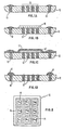
- a processed, sintered MLC substrate 12 bears patterns 13 of exposed metallurgy on its surface.
- the subject invention relates to plating/metallizing the exposed metal of the patterns of metallurgy found on the substrate.
- the pattern of metallurgy concerned may be solely on one surface of the substrate, may be found on several surfaces and/or may penetrate many layers of the structure.
- the Figures illustrate in top view and in cut-away cross-section, only the surface of the metallurgy and the substrate, which are the objects of this invention.
- Substrate 12, as noted above, may contain several patterns of metallurgical features serving differing purposes.
- the metallurgical pattern on the surface is created from the via formation and screening steps and is generally a molybdenum- based metallurgy.
- Molybdenum does not, traditionally, provide the best adhesion qualities for soldered or brazed electrical connection.
- the molybdenum will oxidize and undergo reactive corrosion when exposed to humidity if not provided with a protective coating. Therefore, the molybdenum metallurgical pads are "pretreated" as is described by Kumar, et al in US-A-4,493,856, herein incorporated by reference.
- Kumar, et al teaches the deposition of, for example, nickel, a metal having excellent adhesion characteristics with molybdenum, then a thin flash gold layer to prevent oxidation of the nickel.
- the Ni-Au treatment of all of the metallurgy pads provides both the protection and brazeable/solder- able characteristics desired.
- the pattern of metallurgy 13 found at locations 14 is that metal to which the integrated circuit chips will be connected, referred to as chip mounting or I/O pads.
- the I/O pads bear the very thin coating of protective and conductive metal discussed above.
- the thin gold is necessary on the I/O pads for mounting the chips to the existing metallurgy by solder bonding.
- the other metallurgical pattern comprises the engineering change, EC, pads, 15, associated with the substrate.
- the EC pads provide alternate electrical pathways to the I/O metallurgy and the substrate by the application thereto of interconnecting wires to accommodate engineering changes, testing and defect correction. Given the repeated uses envisioned for any one EC pad, it is preferred that an additional heavy layer of gold be associated with the EC pads.
- masks For application of the metal to the pads alone, without concurrently coating the substrate, masks have been utilized.
- the difficulty in using masks is that the non-uniform shrinkage of the substrate during sintering makes it virtually impossible to achieve registration of a mask with the sintered substrate.
- Selective plating by electroplating may also be employed; but it is somewhat limited in its applicability to EC pads since EC pads are frequently "floating" and cannot therefore be electrically connected for the electroplating process.
- Metallization by the use of diffusion techniques as described in 4,442,137 of Kumar, can assure that each pad is adequately coated while metal deposited on the surrounding substrate area is easily and properly removed.
- the metal is applied to the entire patterned substrate surface, as by sputtering or vapor deposition.
- the metal-coated substrate is then heated to a temperature sufficient to diffuse the metal into the underlying pattern.
- the metal which is overlying non-patterned areas is caused to flake or spall and consequently is easily removed from the now metallized patterned substrate.
- This maskless cladding process avoids the difficulties of correct mask registration and repeated depositing, masking, and etching steps.
- a metal mask again, has the problem of alignment and registration with a sintered, cambered substrate. Resists such as well-known photoresists or E-beam resists cannot survive the deposition, e.g. sputtering, temperatures. Common lithographic materials degrade or shrivel at the processing temperatures of > 250 ° C reached during, for example, sputtering, and thereby fail to effectively shield the masked areas from gold deposition.
- a suitable masking material enabling one to provide an isolation barrier over the I/O pads while depositing heavy gold on the EC pads and substrate using a maskless cladding process.
- a paste is formulated of alumina including a depolymerizable polymer binder and a solvent.
- the paste is screened, sprayed or otherwise selectively deposited onto the area to be protected, as illustrated in Fig. 1B at reference numeral 16.
- the polymer binder enables the paste to be readily applied and to adhere to the surface of the substrate and/or metallurgy to be protected. After screening, the paste is allowed to dry at room temperature to expel the solvent, followed by an accelerated drying step to drive off the polymer binder by "unzipping", or depolymerizing, the same.
- the heavy metal deposition may now be performed using vapor deposition, sputtering or other known technique resulting in a continuous coating 17 over the entire substrate 12, including the metallurgy intended to be plated, here the EC pads 15 of Fig. 1 C, the exposed substrate surface, and the protective coating 16'. Subsequent diffusion processing may proceed in the establishd manner, found in the Kumar patent 4,442,137.
- the isolation barrier layer, 16' has both the mechanical and thermal integrity to withstand the weight of the thick metal layer and the temperatures achieved for diffusing the metal layer to the underlying metallurgy and debonding it with the substrate.
- the substrate is "patterned" in accordance with Kumar's teachings of 4,442,137.
- the "patterning”, for example by ultrasonic horn exposure, results in the removal of the debonded or spalled metal found on the adjacent bare substrate surface, removes the overlying metal in the shielded area and also effects the removal of the inorganic barrier layer 16'.
- the result, as intended, is a clean substrate having selectively coated metallurgical patterns prepared for chip mounting and further connection and use.
- the formulation of the isolation barrier material comprises a unique combination of ingredients to yield the thermal and mechanical characteristics desired.
- the inorganic base of ceramic for example alumina or glass ceramic, must, once solvents and binders are removed, be solid and impermeable enough to support the gold or other metal layer away from the underlying protected metallurgy.
- the inorganic ceramic cannot effectively be deposited directly on the substrate so the depolymerizable polymer binder and solvent are mixed to form the screenable, sprayable or otherwise applicable paste.
- a low vapor pressure solvent, such as amylacetate, is recommended for use if the barrier material is to be applied by screening. A more volatile solvent would clog the screens during application.
- the polymer binder must be one of a group which is readily decomposable at a known temperature so as to depolymerize leaving no carbonaceous residue on the substrate or on the barrier layer.
- suitable polymers include polymethylmethacrylate and other methylmethacrylates, acrylates and copolymers; polyal- phamethylstyrene; polyisobutylene and low temperature decomposing nitrocellulose or polyphthalalde- hyde.
- a step may be taken to heat the applied barrier layer in order to depolymerize the polymer, essentially purging the inorganic layer before metal deposition. It is, however, possible to forego that heating step.
- the polymer chosen such as pojymethyimethacryiate, may decompose during the diffusion step at the diffusion temperatures of 350 ° C - 450 ° C, serving the same function and leaving the organic-free ceramic particulate structure to support the heavy metal layer and isolate the underlying metallurgy.
- a suitable sample formulation consists of
Landscapes
- Engineering & Computer Science (AREA)
- Chemical & Material Sciences (AREA)
- Manufacturing & Machinery (AREA)
- Microelectronics & Electronic Packaging (AREA)
- Chemical Kinetics & Catalysis (AREA)
- Materials Engineering (AREA)
- Mechanical Engineering (AREA)
- Metallurgy (AREA)
- Organic Chemistry (AREA)
- Manufacturing Of Printed Wiring (AREA)
- Parts Printed On Printed Circuit Boards (AREA)
Claims (12)
Applications Claiming Priority (2)
| Application Number | Priority Date | Filing Date | Title |
|---|---|---|---|
| US06/666,954 US4582722A (en) | 1984-10-30 | 1984-10-30 | Diffusion isolation layer for maskless cladding process |
| US666954 | 1984-10-30 |
Publications (3)
| Publication Number | Publication Date |
|---|---|
| EP0180091A2 EP0180091A2 (fr) | 1986-05-07 |
| EP0180091A3 EP0180091A3 (en) | 1987-01-14 |
| EP0180091B1 true EP0180091B1 (fr) | 1990-02-21 |
Family
ID=24676216
Family Applications (1)
| Application Number | Title | Priority Date | Filing Date |
|---|---|---|---|
| EP85113096A Expired - Lifetime EP0180091B1 (fr) | 1984-10-30 | 1985-10-15 | Procédé pour déposer sélectivement des couches métalliques sur un substrat |
Country Status (10)
| Country | Link |
|---|---|
| US (1) | US4582722A (fr) |
| EP (1) | EP0180091B1 (fr) |
| JP (1) | JPH0738420B2 (fr) |
| KR (1) | KR900000438B1 (fr) |
| CN (1) | CN85107549B (fr) |
| AU (1) | AU569805B2 (fr) |
| BR (1) | BR8504923A (fr) |
| CA (1) | CA1267990A (fr) |
| DE (1) | DE3576098D1 (fr) |
| DK (1) | DK495885A (fr) |
Families Citing this family (12)
| Publication number | Priority date | Publication date | Assignee | Title |
|---|---|---|---|---|
| US4582722A (en) * | 1984-10-30 | 1986-04-15 | International Business Machines Corporation | Diffusion isolation layer for maskless cladding process |
| DE3517965A1 (de) * | 1985-05-18 | 1986-11-20 | Robert Bosch Gmbh, 7000 Stuttgart | Verfahren zur herstellung einer elektrischen schaltung in hybridtechnik |
| US4663186A (en) * | 1986-04-24 | 1987-05-05 | International Business Machines Corporation | Screenable paste for use as a barrier layer on a substrate during maskless cladding |
| US4829020A (en) * | 1987-10-23 | 1989-05-09 | The United States Of America As Represented By The United States Department Of Energy | Substrate solder barriers for semiconductor epilayer growth |
| NL9000545A (nl) * | 1990-03-09 | 1991-10-01 | Philips Nv | Werkwijze voor het vervaardigen van geleidersporen. |
| DE4344061C1 (de) * | 1993-12-23 | 1995-03-30 | Mtu Muenchen Gmbh | Bauteil mit Schutzanordnung gegen Alitieren oder Chromieren beim Gasdiffusionsbeschichten und Verfahren zu seiner Herstellung |
| US5787578A (en) * | 1996-07-09 | 1998-08-04 | International Business Machines Corporation | Method of selectively depositing a metallic layer on a ceramic substrate |
| JP2000203885A (ja) * | 1999-01-11 | 2000-07-25 | Ulvac Japan Ltd | 機能性薄膜、機能性基板、及び酸化チタン薄膜製造方法。 |
| WO2002092242A1 (fr) * | 2001-05-16 | 2002-11-21 | Board Of Regents | Depot selectif de matieres pour la fabrication d'interconnexions et de contacts sur des dispositifs semi-conducteurs |
| US6650016B1 (en) * | 2002-10-01 | 2003-11-18 | International Business Machines Corporation | Selective C4 connection in IC packaging |
| US8935981B2 (en) | 2010-09-24 | 2015-01-20 | Canon Nanotechnologies, Inc. | High contrast alignment marks through multiple stage imprinting |
| US20150290713A1 (en) * | 2012-09-13 | 2015-10-15 | Eckart America Corporation | Methods for Producing Platelet Materials |
Family Cites Families (15)
| Publication number | Priority date | Publication date | Assignee | Title |
|---|---|---|---|---|
| US2788289A (en) * | 1951-06-29 | 1957-04-09 | Climax Molybdenum Co | Method of forming protective coatings for molybdenum and molybdenum-base alloys |
| US3741735A (en) * | 1964-01-08 | 1973-06-26 | Atomic Energy Commission | Coating molybdenum with pure gold |
| FR1554958A (fr) * | 1967-02-22 | 1969-01-24 | ||
| US3518756A (en) * | 1967-08-22 | 1970-07-07 | Ibm | Fabrication of multilevel ceramic,microelectronic structures |
| JPS5938268B2 (ja) * | 1974-03-22 | 1984-09-14 | カンザキセイシ カブシキガイシヤ | 新規フタリド化合物の製造法 |
| JPS5159274A (en) * | 1974-11-20 | 1976-05-24 | Tdk Electronics Co Ltd | Hakumakusoshino seizohoho |
| US3957552A (en) * | 1975-03-05 | 1976-05-18 | International Business Machines Corporation | Method for making multilayer devices using only a single critical masking step |
| JPS5248992A (en) * | 1975-10-17 | 1977-04-19 | Nec Corp | Method for manufacturing high frequency elastic surface wave electrode like grating |
| US4293587A (en) * | 1978-11-09 | 1981-10-06 | Zilog, Inc. | Low resistance backside preparation for semiconductor integrated circuit chips |
| US4206254A (en) * | 1979-02-28 | 1980-06-03 | International Business Machines Corporation | Method of selectively depositing metal on a ceramic substrate with a metallurgy pattern |
| US4273859A (en) * | 1979-12-31 | 1981-06-16 | Honeywell Information Systems Inc. | Method of forming solder bump terminals on semiconductor elements |
| US4442137A (en) * | 1982-03-18 | 1984-04-10 | International Business Machines Corporation | Maskless coating of metallurgical features of a dielectric substrate |
| US4493856A (en) * | 1982-03-18 | 1985-01-15 | International Business Machines Corporation | Selective coating of metallurgical features of a dielectric substrate with diverse metals |
| US4526859A (en) * | 1983-12-12 | 1985-07-02 | International Business Machines Corporation | Metallization of a ceramic substrate |
| US4582722A (en) * | 1984-10-30 | 1986-04-15 | International Business Machines Corporation | Diffusion isolation layer for maskless cladding process |
-
1984
- 1984-10-30 US US06/666,954 patent/US4582722A/en not_active Expired - Fee Related
-
1985
- 1985-09-12 JP JP60200731A patent/JPH0738420B2/ja not_active Expired - Lifetime
- 1985-09-18 CA CA000490982A patent/CA1267990A/fr not_active Expired - Lifetime
- 1985-09-26 AU AU47912/85A patent/AU569805B2/en not_active Ceased
- 1985-10-07 BR BR8504923A patent/BR8504923A/pt unknown
- 1985-10-14 CN CN85107549A patent/CN85107549B/zh not_active Expired
- 1985-10-15 EP EP85113096A patent/EP0180091B1/fr not_active Expired - Lifetime
- 1985-10-15 KR KR1019850007591A patent/KR900000438B1/ko not_active Expired
- 1985-10-15 DE DE8585113096T patent/DE3576098D1/de not_active Expired - Lifetime
- 1985-10-29 DK DK495885A patent/DK495885A/da not_active Application Discontinuation
Also Published As
| Publication number | Publication date |
|---|---|
| DE3576098D1 (de) | 1990-03-29 |
| JPH0738420B2 (ja) | 1995-04-26 |
| KR860003650A (ko) | 1986-05-28 |
| AU4791285A (en) | 1986-05-08 |
| CN85107549B (zh) | 1988-05-25 |
| US4582722A (en) | 1986-04-15 |
| EP0180091A2 (fr) | 1986-05-07 |
| AU569805B2 (en) | 1988-02-18 |
| KR900000438B1 (ko) | 1990-01-30 |
| DK495885D0 (da) | 1985-10-29 |
| BR8504923A (pt) | 1986-07-22 |
| EP0180091A3 (en) | 1987-01-14 |
| JPS61107750A (ja) | 1986-05-26 |
| CN85107549A (zh) | 1986-08-13 |
| CA1267990A (fr) | 1990-04-17 |
| DK495885A (da) | 1986-05-01 |
Similar Documents
| Publication | Publication Date | Title |
|---|---|---|
| CA1189748A (fr) | Enduction sans masque des zones metallisees d'un substrat dielectrique | |
| EP0144046B1 (fr) | Procédé pour la formation d'un dessin métallurgique à surface densifiée sur ou dans un substrat fritté diélectrique | |
| EP0006810B1 (fr) | Procédé de fabrication d'un circuit intégré hybride | |
| US4582722A (en) | Diffusion isolation layer for maskless cladding process | |
| JPH0684546B2 (ja) | 電子部品 | |
| US4206254A (en) | Method of selectively depositing metal on a ceramic substrate with a metallurgy pattern | |
| JPH0150119B2 (fr) | ||
| US5787578A (en) | Method of selectively depositing a metallic layer on a ceramic substrate | |
| JPS6377787A (ja) | プリント配線板製造用マスク及びその製造方法 | |
| JPS5818961B2 (ja) | セラミツク基板上に耐火性冶金属を形成する方法 | |
| JPS6317337B2 (fr) | ||
| US4786674A (en) | Diffusion isolation layer for maskless cladding process | |
| CA1312405C (fr) | Couche d'isolation par diffusion pour operations de revetement metallique sans masque | |
| EP0242558B1 (fr) | Pâte de sérigraphie utilisable comme couche de barrière sur un substrat pendant le revêtement sans masque | |
| JPS5933665B2 (ja) | 応力のないニツケル層を与える方法 | |
| US5613181A (en) | Co-sintered surface metallization for pin-join, wire-bond and chip attach | |
| US6471805B1 (en) | Method of forming metal contact pads on a metal support substrate | |
| JP3554195B2 (ja) | 配線基板 | |
| JPH01272192A (ja) | セラミックス基板 | |
| JPS61245555A (ja) | 半導体用端子接続構体 | |
| JPS6182493A (ja) | セラミツク配線基板の製造方法 | |
| JPH01181499A (ja) | セラミック配線板 | |
| JPS63244697A (ja) | 回路基板 | |
| JPH0451587A (ja) | 配線基板の製造方法 | |
| JPH0256991A (ja) | 印刷配線板の製造方法 |
Legal Events
| Date | Code | Title | Description |
|---|---|---|---|
| PUAI | Public reference made under article 153(3) epc to a published international application that has entered the european phase |
Free format text: ORIGINAL CODE: 0009012 |
|
| AK | Designated contracting states |
Kind code of ref document: A2 Designated state(s): CH DE FR GB IT LI NL SE |
|
| 17P | Request for examination filed |
Effective date: 19860819 |
|
| PUAL | Search report despatched |
Free format text: ORIGINAL CODE: 0009013 |
|
| AK | Designated contracting states |
Kind code of ref document: A3 Designated state(s): CH DE FR GB IT LI NL SE |
|
| 17Q | First examination report despatched |
Effective date: 19881003 |
|
| GRAA | (expected) grant |
Free format text: ORIGINAL CODE: 0009210 |
|
| AK | Designated contracting states |
Kind code of ref document: B1 Designated state(s): CH DE FR GB IT LI NL SE |
|
| REF | Corresponds to: |
Ref document number: 3576098 Country of ref document: DE Date of ref document: 19900329 |
|
| ET | Fr: translation filed | ||
| ITF | It: translation for a ep patent filed | ||
| PLBE | No opposition filed within time limit |
Free format text: ORIGINAL CODE: 0009261 |
|
| STAA | Information on the status of an ep patent application or granted ep patent |
Free format text: STATUS: NO OPPOSITION FILED WITHIN TIME LIMIT |
|
| 26N | No opposition filed | ||
| ITTA | It: last paid annual fee | ||
| PGFP | Annual fee paid to national office [announced via postgrant information from national office to epo] |
Ref country code: CH Payment date: 19950119 Year of fee payment: 10 |
|
| EAL | Se: european patent in force in sweden |
Ref document number: 85113096.3 |
|
| PGFP | Annual fee paid to national office [announced via postgrant information from national office to epo] |
Ref country code: SE Payment date: 19951002 Year of fee payment: 11 |
|
| PGFP | Annual fee paid to national office [announced via postgrant information from national office to epo] |
Ref country code: DE Payment date: 19951030 Year of fee payment: 11 |
|
| PG25 | Lapsed in a contracting state [announced via postgrant information from national office to epo] |
Ref country code: LI Effective date: 19951031 Ref country code: CH Effective date: 19951031 |
|
| PGFP | Annual fee paid to national office [announced via postgrant information from national office to epo] |
Ref country code: NL Payment date: 19951031 Year of fee payment: 11 |
|
| REG | Reference to a national code |
Ref country code: CH Ref legal event code: PL |
|
| PGFP | Annual fee paid to national office [announced via postgrant information from national office to epo] |
Ref country code: GB Payment date: 19960925 Year of fee payment: 12 |
|
| PGFP | Annual fee paid to national office [announced via postgrant information from national office to epo] |
Ref country code: FR Payment date: 19961007 Year of fee payment: 12 |
|
| PG25 | Lapsed in a contracting state [announced via postgrant information from national office to epo] |
Ref country code: SE Effective date: 19961016 |
|
| PG25 | Lapsed in a contracting state [announced via postgrant information from national office to epo] |
Ref country code: NL Effective date: 19970501 |
|
| NLV4 | Nl: lapsed or anulled due to non-payment of the annual fee |
Effective date: 19970501 |
|
| PG25 | Lapsed in a contracting state [announced via postgrant information from national office to epo] |
Ref country code: DE Effective date: 19970701 |
|
| EUG | Se: european patent has lapsed |
Ref document number: 85113096.3 |
|
| PG25 | Lapsed in a contracting state [announced via postgrant information from national office to epo] |
Ref country code: GB Free format text: LAPSE BECAUSE OF NON-PAYMENT OF DUE FEES Effective date: 19971015 |
|
| PG25 | Lapsed in a contracting state [announced via postgrant information from national office to epo] |
Ref country code: FR Free format text: THE PATENT HAS BEEN ANNULLED BY A DECISION OF A NATIONAL AUTHORITY Effective date: 19971031 |
|
| GBPC | Gb: european patent ceased through non-payment of renewal fee |
Effective date: 19971015 |
|
| REG | Reference to a national code |
Ref country code: FR Ref legal event code: ST |