EP0182719A2 - Mémoire semi-conductrice avec des registres de décalage pour lecture et écriture à grande vitesse - Google Patents
Mémoire semi-conductrice avec des registres de décalage pour lecture et écriture à grande vitesse Download PDFInfo
- Publication number
- EP0182719A2 EP0182719A2 EP85402246A EP85402246A EP0182719A2 EP 0182719 A2 EP0182719 A2 EP 0182719A2 EP 85402246 A EP85402246 A EP 85402246A EP 85402246 A EP85402246 A EP 85402246A EP 0182719 A2 EP0182719 A2 EP 0182719A2
- Authority
- EP
- European Patent Office
- Prior art keywords
- shift register
- data
- shift registers
- word line
- parallel data
- Prior art date
- Legal status (The legal status is an assumption and is not a legal conclusion. Google has not performed a legal analysis and makes no representation as to the accuracy of the status listed.)
- Granted
Links
Images





Classifications
-
- G—PHYSICS
- G11—INFORMATION STORAGE
- G11C—STATIC STORES
- G11C7/00—Arrangements for writing information into, or reading information out from, a digital store
- G11C7/10—Input/output [I/O] data interface arrangements, e.g. I/O data control circuits, I/O data buffers
- G11C7/1075—Input/output [I/O] data interface arrangements, e.g. I/O data control circuits, I/O data buffers for multiport memories each having random access ports and serial ports, e.g. video RAM
Definitions
- the present invention relates to a semiconductor memory device, more particularly to a random access memory (RAM) with a shift register for high-speed reading and writing.
- the RAM according to the present invention can be used for a video RAM.
- High-speed read/write shift registers are used in a video RAM for storing the picture data for a cathode ray tube (CRT) display in order to treat a large amount of data in a short time.
- CTR cathode ray tube
- a semiconductor memory device including: a RAM having a memory cell array, a plurality of bit lines, and a plurality of word lines; a pair of shift registers adapted to be connected with the plurality of bit lines; transfer gate units arranged between the plurality of bit lines and the shift registers; and parallel data transfer unit being provided between the shift registers for carrying out the parallel data transfer between the shift registers.
- a semiconductor memory device including: a RAM having a memory cell array, a plurality of bit lines, and a plurality of word lines; a shift register for output for carrying out serial reading, data for one word line registered in parallel from the memory cell array into said shift register for output being delivered serially from the shift register for output; a shift register for input for registering data for one word line supplied serially from an external data source; a parallel data transfer unit for carrying out logic processing of the data registered in the shift register for output and the shift register for input; and an instruction decoder for delivering an instruction for a selected logic which should be executed in the parallel data transfer unit; the data for one word line to be supplied to the shift register for input and an operation code for instructing a selected logic to be supplied to the instruction decoder being able to be serially transmitted; the data for one word line obtained as a result of the processing in the parallel data transfer unit according to the instructed selected logic being able to be written into the memory cells of a selected word line in the memory
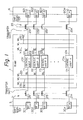
- Fig. 1 shows a prior art semiconductor memory device with shift registers
- the device of Fig. 1 includes a dynamic RAM 1 of the open bit-line type, groups of transfer gates 21 and 23, and shift registers 3 and 6.
- the RAM 1 includes sense amplifiers 101, 102, 103, ... 10n, bit lines (BL) 111, 112, 113, ... lln, bit lines (BL) 121, 122, 123, ... 12n, word lines (WL) 131, 132, 133, ... 13n; 141, 142, 143, ... 14n.
- Memory cells (not shown) are provided at the crosses of the bit lines and the word lines.
- the shift register 3 includes the sequence of elements (bits) 301, 302, 303, ... 30n, the number n being, for example, 256.
- the elements 301, 302, 303, ... 30n are connected through the transfer gates 211, 212, 213, ... 21n to the bit lines 111, 112, 113, ... lln of the RAM 1.
- the elements 601, 602, 603, ... 60n of the shift register 6 are connected through the transfer gates 231, 232, 233, ... 23n to the bit lines 121, 122, 123, ... 12n of the RAM 1.
- the data in the shift register 3 are delivered from the shift register 3 in a serial form.
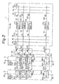
- a semiconductor memory device with shift registers according to an embodiment of the present invention is shown in Fi g . 2.
- the device of Fig. 2 includes a dynamic RAM 1 of the open bit-line type, groups of transfer gates 21 and 22, and shift registers 3 and 4.
- the data are supplied through the input lines 32 and 42 of the shift registers 3 and 4.
- the data are delivered through the output lines 33 and 43 from the shift registers 3 and 4. If the shift register 3 is used, for example, exclusively for reading, the input line 32 can be omitted. If the shift register 4 is used, for example, exclusively for writing, the output line 43 can be omitted.
- the RAM 1 includes sense amplifiers 101, 102, 103, ... lOn, bit lines (BL) 111, 112, 113, ... lln, bit lines (BL) 121, 122, 123, ... 12n, word lines (WL) 131, 132, 133, ... 13n; 141, 142, 143, ... 14n.
- Memory cells (not shown) are provided at the crosses of the bit lines and the word lines.
- a pair of data buses (not shown) are provided along the sense amplifiers 101, 102, 103, ... lOn for writing or reading the data.
- the shift register 3 includes the sequence of elements (bits) 301, 302, 303, ... 30n and shift register gates 511, 512, 513, ...
- the shift register 4 includes the sequence of elements (bits) 401, 402, 403, ... 40n and shift register gates 521, 522, 523, ... 52(n-l). Between the elements 301, 302, 303, ... 30n of the shift register 3 and the elements 401, 402, 403, ... 40n of the shift register 4, there are provided shift register gates 501, 502, 503, ... 50n.
- the shift register gates are represented as Gl between the adjacent elements BIT(i) and BIT(i+l) of the shift register 3 (shift register A), G2 between the adjacent elements BIT(i) and BIT(i+l) of the shift register 4 (shift register B), G3 between the input terminal of the element BIT(i+l) of the shift register 3 and the output terminal of the element BIT(I) of the shift register 4, and G4 between the output terminal of the element BIT(i) of the shift register 3 and the input terminal of the element BIT(i+l) of the shift register 4.
- the shift register gates Gl and G2 should be in the ON state, while the shift register gates G3 and G4 should be in the OFF state.
- the shift register gates Gl and G3 should be in the ON state, while the shift register gates G2 and G4 should be in the OFF state.
- the shift register gates G2 and G4 should be in the ON state, while the shift register gates Gl and G3 should be in the OFF state.
- the device of Fig. 1 including the circuit of Fig. 2 can be used for a scroll display operation in the upward direction in the cathode ray tube (CRT) display.
- the shift register 3 is used for the reading, while the shift register 4 is used for the writing.
- the data for one word line is transferred first to the shift register 3, and next to the shift register 4.
- shift operation of the shift register 3 takes place, so that the video signal is supplied to the CRT and the data of the shift register 4 is supplied to the immediately preceding word line for which the scanning has a already been completed. This operation is successively repeated.
- the scroll display operation in the upward direction is carried out.
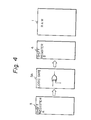
- FIG. 4 and 5 Modified embodiments of the present invention are shown in Figs. 4 and 5.
- logic gates 5A and 5B are provide between the shift registers 3 and 4.
- the display of a negative picture based on a positive picture can be carried out quickly by using the devices of Figs. 4 and 5.
- the logic gates 5A and 5B consist of exclusive OR gates.
- the OR gates operate as "through” elements when one of the input signals is “0" and operate as inverter elements when one of the input signals is “1".
- the logic gate 5A After registering one word line data of RAM 1 in the shift register 3, the logic gate 5A, if applied with "1" at each one input of its each exclusive OR gate, inverts the data in the shift register 3 and transfers the thus-inverted data to the shift register 4 in parallel, and the data are written in the memory cells of the selected word line through the shift register 4. Alternatively, the data can be read out through the shift register 4 to the exterior. By carrying out this operation over all of the picture of the display, inversion between the positive picture and negative picture is realized quickly. If selection of a word line is changed, displacement of the picture is also realized.
- the device shown in Fig. 5 having the shift register 3' (shift register C) is suitable for supplying a control input signal to one of the input terminals of the exclusive OR gates.
- shift register C shift register C
- each of two shift registers is associated exclusively with one of the portions of the RAM, it is possible to carry out data exchange between the two shift registers.
- FIG. 6 A further modified embodiment of the present invention is shown in Fig. 6.
- the system of the RAM in the device shown in Fig. 6 includes the memory cell array 71 having bit lines (BL), word lines (WL), and memory cells (not shown); the shift register 73 for input; the shift register 74 for output; the parallel data transfer circuit 751; the operation code (OP code) decoder 752; the input/output gate 76; the column decoder 77; and the word decoder 78.
- the system of the RAM is connected with the central processor unit (CPU) 70.
- CPU central processor unit
- Serial data are transmitted from the CPU 70 through the transmission line to the shift register 73 for input and the operation code decoder 752.
- the parallel data transfer circuit 751 carries out the logic processing of the data registered in the shift register 73 for input and the shift register 74 for output to generate new data for one word line.
- the parallel data transfer circuit 751 has logic functions such as AND and OR.
- the selection of the logic function of the parallel data transfer circuit 751 is designated by the output of the operation code decoder 752.
- the operation code for designating the logic processing to be selected is transmitted together with the data for one word line from the CPU 70 through the transmission line to the operation code decoder 752, where the sent operation code is decoded to be supplied to the parallel data transfer circuit 751.
- the operation code decoder 752 and the parallel data transfer circuit 751 are connected through n signal lines, n being the number of kinds of logic processing.
- the designation of the selected kind of logic processing is carried out by turning HIGH the potential of the signal line corresponding to the selected kind of logic processing.
- the data for one word line which is to be supplied to the shift register 73 for input is determined by the logic processing which is to be applied to the picture data stored in the memory cell array 71. If the OR logic is determined, the result of the OR logic processing with regard to the new picture data supplied to the shift register 73 for input is the superposition of the old and new pictures.
- the parallel data transfer circuit 751 acts as a circuit for detecting the blue line data and changing the detected blue line data into red line data.
- the data supplied to the shift register 73 for input is data such as mask data, which instructs in which portion of the word lines the processing in question should be executed.
- FIG. 7 A still further modified embodiment of the present invention is shown in Fig. 7.
- the device of Fig. 7 is designed for the case where one pixel is represented by 8 bits.
- one pixel of a color picture consists of at least 3 bits, that is, R, G, and B
- one pixel of a monochromic picture consists of plural bits if the monochromic picture has a varieties of color densities.
- Such a situation can be dealt with by providing as many of the memory cell array 81, the shift register 83 for input, the shift register 84 for output, and parallel data transfer circuit 85 as the number of bits for one pixel.
- the parallel data transferring circuit 85 consists of the assemblies of the parallel data transferring circuits 85(1), 85(2), 85(3), and so on.
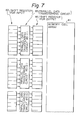
- FIG. 8 An example of the serial data used in the device of Fig. 7 is shown in Fig. 8.
- the beginning 8 bits are the operating bits, that is, the operating code.
- Each of the former 4 bits (BIT 0 to BIT 3) and the latter 4 bits (BIT 4 to BIT 7) has the value of 0 to 9, A, B, C, D, E, or F in the hexadecimal number system.
- An example of the instructions represented by the operating bits is shown in Fig. 7.
- the data bits for one word line follow the operating bits BIT 0 to BIT 7 shown in Fig. 7.
- the input line 731 (Fig. 6) can be used both for the operating code and the data so that the number of the external terminals of the system of RAM need not by increased.
- the device of Fig. 7 has the usual read/write mode using a data bus, the serial read mode using a shift register for output, and the serial write mode using a shift register for input.
- serial data S(IN) having the format of Fig. 8 are delivered from the CPU 70 through the S(IN) transmission line.
- the operation code decoder 752 Upon receipt of the serial data S(IN), the operation code decoder 752 decodes the beginning 8 bits, which is the operating code, and the output of the operation code decoder 752 carries out the selection of the processing in the parallel data transfer circuit 751 according to the instructions shown in Fig. 9.
- the data bits of the serial data S(IN) for one word line are registered in the shift register 73 for input.
- the operating code is automatically shifted out from the shift register 73 for input.
- the processing in the parallel data transfer circuit 751 is started after the data bits for one word line are registered in the shift register 73 for input.
- the new data resulting from the processing are written in parallel in the memory cell array connected to the selected word line in the memory cell array 71.
- the operation is the updating of the picture data.
- the operation includes scrolling of the picture in addition to the updating of the picture data.
- Parallel transmission lines are provided between the shift register 74 for output and the memory cell array 71. Hence, the new data resulting from the processing are first registered in the shift register 74 for output and subsequently written in the corresponding word line in the memory cell array 71.
Landscapes
- Engineering & Computer Science (AREA)
- Multimedia (AREA)
- Dram (AREA)
Applications Claiming Priority (4)
| Application Number | Priority Date | Filing Date | Title |
|---|---|---|---|
| JP245802/84 | 1984-11-20 | ||
| JP59245802A JPS61123875A (ja) | 1984-11-20 | 1984-11-20 | 半導体記憶装置 |
| JP59275553A JPS61149989A (ja) | 1984-12-25 | 1984-12-25 | 半導体記憶装置 |
| JP275553/84 | 1984-12-25 |
Publications (3)
| Publication Number | Publication Date |
|---|---|
| EP0182719A2 true EP0182719A2 (fr) | 1986-05-28 |
| EP0182719A3 EP0182719A3 (en) | 1988-08-03 |
| EP0182719B1 EP0182719B1 (fr) | 1991-10-09 |
Family
ID=26537411
Family Applications (1)
| Application Number | Title | Priority Date | Filing Date |
|---|---|---|---|
| EP85402246A Expired - Lifetime EP0182719B1 (fr) | 1984-11-20 | 1985-11-20 | Mémoire semi-conductrice avec des registres de décalage pour lecture et écriture à grande vitesse |
Country Status (4)
| Country | Link |
|---|---|
| US (1) | US4745577A (fr) |
| EP (1) | EP0182719B1 (fr) |
| KR (1) | KR900000632B1 (fr) |
| DE (1) | DE3584352D1 (fr) |
Cited By (10)
| Publication number | Priority date | Publication date | Assignee | Title |
|---|---|---|---|---|
| EP0260503A1 (fr) * | 1986-09-02 | 1988-03-23 | Fujitsu Limited | Dispositif mémoire à semi-conducteurs |
| EP0282650A1 (fr) * | 1986-12-25 | 1988-09-21 | Nec Corporation | Mémoire à semi-conducteurs avec arrangement des cellules |
| DE3733012A1 (de) * | 1987-09-30 | 1989-04-13 | Thomson Brandt Gmbh | Speicheranordnung |
| FR2623320A1 (fr) * | 1987-11-18 | 1989-05-19 | Sony Corp | Memoire de type dynamique |
| GB2224588A (en) * | 1988-09-23 | 1990-05-09 | Broadcast Television Syst | Multiplexed memory system |
| EP0355851A3 (fr) * | 1988-08-25 | 1990-05-09 | Kabushiki Kaisha Toshiba | RAM dynamique pour le stockage des trames vidéo |
| EP0326172A3 (fr) * | 1988-01-29 | 1991-11-21 | Nec Corporation | Circuit de mémoire avec un dispositif de circuit d'accés sériel |
| EP0653761A2 (fr) | 1993-11-11 | 1995-05-17 | Oki Electric Industry Company, Limited | Une mémoire à accès séquentiel |
| US6278644B1 (en) | 1999-09-06 | 2001-08-21 | Oki Electric Industry Co., Ltd. | Serial access memory having data registers shared in units of a plurality of columns |
| KR100338270B1 (ko) * | 1993-11-11 | 2002-10-11 | 오끼 덴끼 고오교 가부시끼가이샤 | 시리얼액세스메모리와데이터전송방법 |
Families Citing this family (16)
| Publication number | Priority date | Publication date | Assignee | Title |
|---|---|---|---|---|
| US4876663A (en) * | 1987-04-23 | 1989-10-24 | Mccord Donald G | Display interface system using buffered VDRAMs and plural shift registers for data rate control between data source and display |
| JPH0760594B2 (ja) * | 1987-06-25 | 1995-06-28 | 富士通株式会社 | 半導体記憶装置 |
| JP2501344B2 (ja) * | 1987-12-26 | 1996-05-29 | 株式会社東芝 | デ―タ転送回路 |
| JPH0283899A (ja) * | 1988-09-20 | 1990-03-23 | Fujitsu Ltd | 半導体記憶装置 |
| JP2607689B2 (ja) * | 1989-07-10 | 1997-05-07 | 株式会社日立製作所 | ベクトル処理装置 |
| US5426731A (en) * | 1990-11-09 | 1995-06-20 | Fuji Photo Film Co., Ltd. | Apparatus for processing signals representative of a computer graphics image and a real image |
| US5799186A (en) * | 1990-12-20 | 1998-08-25 | Eastman Kodak Company | Method and apparatus for programming a peripheral processor with a serial output memory device |
| US5579484A (en) * | 1991-02-22 | 1996-11-26 | Ncr Corporation | System for performing fast data accessing in multiply/accumulate operations while using a VRAM |
| US6897895B1 (en) * | 1998-05-28 | 2005-05-24 | Sanyo Electric Co., Ltd. | Digital camera |
| US7313639B2 (en) * | 2003-01-13 | 2007-12-25 | Rambus Inc. | Memory system and device with serialized data transfer |
| GB2424105B (en) * | 2003-01-13 | 2007-03-07 | Rambus Inc | Coded write masking |
| US7054202B2 (en) * | 2003-06-03 | 2006-05-30 | Samsung Electronics Co., Ltd. | High burst rate write data paths for integrated circuit memory devices and methods of operating same |
| DE102004026526B4 (de) * | 2003-06-03 | 2010-09-23 | Samsung Electronics Co., Ltd., Suwon | Integrierter Schaltungsbaustein und Betriebsverfahren |
| GB2433626B (en) * | 2003-06-03 | 2007-11-07 | Samsung Electronics Co Ltd | High burst rate write data paths for integrated circuit memory devices and methods of operating same |
| JP5073935B2 (ja) * | 2005-10-06 | 2012-11-14 | オンセミコンダクター・トレーディング・リミテッド | シリアルデータ入力システム |
| US9153305B2 (en) | 2013-08-30 | 2015-10-06 | Micron Technology, Inc. | Independently addressable memory array address spaces |
Family Cites Families (3)
| Publication number | Priority date | Publication date | Assignee | Title |
|---|---|---|---|---|
| NL8202364A (nl) * | 1982-06-11 | 1984-01-02 | Philips Nv | Serie-parallel-serie schuifregistergeheugen, waarbij het parallelopslagregister mede redundante enkelvoudige opslagregisters bevat, en afbeeldtoestel, voorzien van een zodanig georganiseerd beeldgeheugen. |
| JPS59180871A (ja) * | 1983-03-31 | 1984-10-15 | Fujitsu Ltd | 半導体メモリ装置 |
| NL8301603A (nl) * | 1983-05-06 | 1984-12-03 | Philips Nv | Geintegreerde geheugenschakeling van een serie-parallel-serie type. |
-
1985
- 1985-11-15 US US06/798,284 patent/US4745577A/en not_active Expired - Lifetime
- 1985-11-20 DE DE8585402246T patent/DE3584352D1/de not_active Expired - Lifetime
- 1985-11-20 EP EP85402246A patent/EP0182719B1/fr not_active Expired - Lifetime
- 1985-11-20 KR KR1019850008672A patent/KR900000632B1/ko not_active Expired
Cited By (14)
| Publication number | Priority date | Publication date | Assignee | Title |
|---|---|---|---|---|
| US4799197A (en) * | 1986-09-02 | 1989-01-17 | Fujitsu Limited | Semiconductor memory device having a CMOS sense amplifier |
| EP0260503A1 (fr) * | 1986-09-02 | 1988-03-23 | Fujitsu Limited | Dispositif mémoire à semi-conducteurs |
| EP0282650A1 (fr) * | 1986-12-25 | 1988-09-21 | Nec Corporation | Mémoire à semi-conducteurs avec arrangement des cellules |
| DE3733012A1 (de) * | 1987-09-30 | 1989-04-13 | Thomson Brandt Gmbh | Speicheranordnung |
| FR2623320A1 (fr) * | 1987-11-18 | 1989-05-19 | Sony Corp | Memoire de type dynamique |
| US5280448A (en) * | 1987-11-18 | 1994-01-18 | Sony Corporation | Dynamic memory with group bit lines and associated bit line group selector |
| EP0326172A3 (fr) * | 1988-01-29 | 1991-11-21 | Nec Corporation | Circuit de mémoire avec un dispositif de circuit d'accés sériel |
| EP0355851A3 (fr) * | 1988-08-25 | 1990-05-09 | Kabushiki Kaisha Toshiba | RAM dynamique pour le stockage des trames vidéo |
| GB2224588A (en) * | 1988-09-23 | 1990-05-09 | Broadcast Television Syst | Multiplexed memory system |
| EP0653761A2 (fr) | 1993-11-11 | 1995-05-17 | Oki Electric Industry Company, Limited | Une mémoire à accès séquentiel |
| EP0653761A3 (fr) * | 1993-11-11 | 1996-03-06 | Oki Electric Ind Co Ltd | Une mémoire à accès séquentiel. |
| US5812148A (en) * | 1993-11-11 | 1998-09-22 | Oki Electric Industry Co., Ltd. | Serial access memory |
| KR100338270B1 (ko) * | 1993-11-11 | 2002-10-11 | 오끼 덴끼 고오교 가부시끼가이샤 | 시리얼액세스메모리와데이터전송방법 |
| US6278644B1 (en) | 1999-09-06 | 2001-08-21 | Oki Electric Industry Co., Ltd. | Serial access memory having data registers shared in units of a plurality of columns |
Also Published As
| Publication number | Publication date |
|---|---|
| EP0182719B1 (fr) | 1991-10-09 |
| EP0182719A3 (en) | 1988-08-03 |
| KR900000632B1 (ko) | 1990-02-01 |
| US4745577A (en) | 1988-05-17 |
| KR860004466A (ko) | 1986-06-23 |
| DE3584352D1 (de) | 1991-11-14 |
Similar Documents
| Publication | Publication Date | Title |
|---|---|---|
| EP0182719B1 (fr) | Mémoire semi-conductrice avec des registres de décalage pour lecture et écriture à grande vitesse | |
| US4833657A (en) | Semiconductor frame buffer memory | |
| EP0678872B1 (fr) | Dispositif de mémoire à semi-conducteurs | |
| EP0360243B1 (fr) | Dispositif de mémoire vidéo | |
| GB2247387A (en) | Apparatus for storing information in and deriving information from a frame buffer | |
| US5461680A (en) | Method and apparatus for converting image data between bit-plane and multi-bit pixel data formats | |
| KR910002202B1 (ko) | 바운더리-프리 반도체 메모리 장치 | |
| KR880000968A (ko) | 반도체 기억장치 | |
| US4512018A (en) | Shifter circuit | |
| KR900002327B1 (ko) | 칼라 화상 표시 장치 | |
| US4799154A (en) | Array processor apparatus | |
| JPH06208787A (ja) | ランダムアクセスメモリ | |
| US6990039B2 (en) | Semiconductor storing device | |
| JPH06167958A (ja) | 記憶装置 | |
| JPS61149989A (ja) | 半導体記憶装置 | |
| EP0479274A2 (fr) | Dispositif de mémoire à semi-conducteurs | |
| US5678035A (en) | Image data memory control unit | |
| EP0245564A1 (fr) | Mémoire à multiples portes et source pour information de points d'image | |
| JPH0346832B2 (fr) | ||
| KR100201175B1 (ko) | 비디오 ramdacs의 이중센스 증폭기 구조체 | |
| JP2629767B2 (ja) | メモリ装置 | |
| JPS6411991B2 (fr) | ||
| JPS61267792A (ja) | メモリ読出し方式 | |
| JPH05135573A (ja) | 直交メモリ | |
| JPS58166387A (ja) | 画像メモリ読出し方式 |
Legal Events
| Date | Code | Title | Description |
|---|---|---|---|
| PUAI | Public reference made under article 153(3) epc to a published international application that has entered the european phase |
Free format text: ORIGINAL CODE: 0009012 |
|
| AK | Designated contracting states |
Kind code of ref document: A2 Designated state(s): DE FR GB |
|
| PUAL | Search report despatched |
Free format text: ORIGINAL CODE: 0009013 |
|
| AK | Designated contracting states |
Kind code of ref document: A3 Designated state(s): DE FR GB |
|
| 17P | Request for examination filed |
Effective date: 19880924 |
|
| 17Q | First examination report despatched |
Effective date: 19900330 |
|
| GRAA | (expected) grant |
Free format text: ORIGINAL CODE: 0009210 |
|
| AK | Designated contracting states |
Kind code of ref document: B1 Designated state(s): DE FR GB |
|
| REF | Corresponds to: |
Ref document number: 3584352 Country of ref document: DE Date of ref document: 19911114 |
|
| ET | Fr: translation filed | ||
| PLBE | No opposition filed within time limit |
Free format text: ORIGINAL CODE: 0009261 |
|
| STAA | Information on the status of an ep patent application or granted ep patent |
Free format text: STATUS: NO OPPOSITION FILED WITHIN TIME LIMIT |
|
| 26N | No opposition filed | ||
| PGFP | Annual fee paid to national office [announced via postgrant information from national office to epo] |
Ref country code: FR Payment date: 19941109 Year of fee payment: 10 |
|
| PGFP | Annual fee paid to national office [announced via postgrant information from national office to epo] |
Ref country code: GB Payment date: 19941110 Year of fee payment: 10 |
|
| PG25 | Lapsed in a contracting state [announced via postgrant information from national office to epo] |
Ref country code: GB Effective date: 19951120 |
|
| GBPC | Gb: european patent ceased through non-payment of renewal fee |
Effective date: 19951120 |
|
| PG25 | Lapsed in a contracting state [announced via postgrant information from national office to epo] |
Ref country code: FR Effective date: 19960731 |
|
| REG | Reference to a national code |
Ref country code: FR Ref legal event code: ST |
|
| PGFP | Annual fee paid to national office [announced via postgrant information from national office to epo] |
Ref country code: DE Payment date: 20001113 Year of fee payment: 16 |
|
| PG25 | Lapsed in a contracting state [announced via postgrant information from national office to epo] |
Ref country code: DE Free format text: LAPSE BECAUSE OF NON-PAYMENT OF DUE FEES Effective date: 20020702 |