EP0183562A2 - Diodes en polysilicium - Google Patents
Diodes en polysilicium Download PDFInfo
- Publication number
- EP0183562A2 EP0183562A2 EP85308704A EP85308704A EP0183562A2 EP 0183562 A2 EP0183562 A2 EP 0183562A2 EP 85308704 A EP85308704 A EP 85308704A EP 85308704 A EP85308704 A EP 85308704A EP 0183562 A2 EP0183562 A2 EP 0183562A2
- Authority
- EP
- European Patent Office
- Prior art keywords
- polysilicon
- diode
- layer
- sidewall
- silicon dioxide
- Prior art date
- Legal status (The legal status is an assumption and is not a legal conclusion. Google has not performed a legal analysis and makes no representation as to the accuracy of the status listed.)
- Withdrawn
Links
Images


Classifications
-
- H—ELECTRICITY
- H10—SEMICONDUCTOR DEVICES; ELECTRIC SOLID-STATE DEVICES NOT OTHERWISE PROVIDED FOR
- H10D—INORGANIC ELECTRIC SEMICONDUCTOR DEVICES
- H10D62/00—Semiconductor bodies, or regions thereof, of devices having potential barriers
- H10D62/40—Crystalline structures
-
- H—ELECTRICITY
- H10—SEMICONDUCTOR DEVICES; ELECTRIC SOLID-STATE DEVICES NOT OTHERWISE PROVIDED FOR
- H10D—INORGANIC ELECTRIC SEMICONDUCTOR DEVICES
- H10D8/00—Diodes
-
- H—ELECTRICITY
- H10—SEMICONDUCTOR DEVICES; ELECTRIC SOLID-STATE DEVICES NOT OTHERWISE PROVIDED FOR
- H10P—GENERIC PROCESSES OR APPARATUS FOR THE MANUFACTURE OR TREATMENT OF DEVICES COVERED BY CLASS H10
- H10P32/00—Diffusion of dopants within, into or out of wafers, substrates or parts of devices
- H10P32/30—Diffusion for doping of conductive or resistive layers
- H10P32/302—Doping polycrystalline silicon or amorphous silicon layers
-
- Y—GENERAL TAGGING OF NEW TECHNOLOGICAL DEVELOPMENTS; GENERAL TAGGING OF CROSS-SECTIONAL TECHNOLOGIES SPANNING OVER SEVERAL SECTIONS OF THE IPC; TECHNICAL SUBJECTS COVERED BY FORMER USPC CROSS-REFERENCE ART COLLECTIONS [XRACs] AND DIGESTS
- Y10—TECHNICAL SUBJECTS COVERED BY FORMER USPC
- Y10S—TECHNICAL SUBJECTS COVERED BY FORMER USPC CROSS-REFERENCE ART COLLECTIONS [XRACs] AND DIGESTS
- Y10S148/00—Metal treatment
- Y10S148/01—Bipolar transistors-ion implantation
Definitions
- a lateral diode in a film or layer of polysilicon i.e., polycrystalline silicon
- polysilicon i.e., polycrystalline silicon
- such diodes usually have high reverse current leakage if the polysilicon is doped sufficiently to lower the series resistance to provide satisfactory current flow before the diode saturates.
- dopant concentration was discussed by Manoliu et al in "P-N Junctions in Polycrystalline-Silicon Films", Solid State Electronics, Volume 15, 1972, at pages 1103-1106.
- a lateral polysilicon diode comprising: a polysilicon substrate having a first zone sufficiently doped to provide a first semiconductor type; a second zone sufficiently doped to provide a second semiconductor type whereby a junction between the two zones forms a diode; and treated portions on the lateral edges of said diode to inhibit current leakage around the edges of said lateral diode to lower the reverse current leakage of said diode.
- the invention provides a diode constructed of polycrystalline silicon characterised by low reverse current leakage as well as low series resistance wherein reverse current leakage is reduced by repairing the damaged sidewalls of the polysilicon diode as it is formed.
- current leakage is preferably reduced by etching the damaged sidewalls of the polysilicon diode as it is formed to repair damage thereto, and a protective layer of oxide is placed over the repaired sidewalls.
- a polysilicon diode embodying the invention may be fabricated and used with either bipolar or MOS type devices.
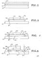
- Figures 2-6 which illustrate the step by step construction of the polysilicon diode, therefore merely illustrate the underlying integrated circuit structure as a substrate 10.
- the substrate 10 representing a typical underlying integrated circuit structure, is shown with a polysilicon layer 20 thereon having a thickness of 3000 to 6000 Angstroms deposited thereon depending upon the desired current carrying capacity of the diode.
- the resulting three layer structure is masked and etched using a suitable plasma etch, such as SF 6 , to etch the nitride, oxide and polysilicon layers leaving behind portion 22 of the polysilicon layer, together with, respectively, portions 32 and 42 of the oxide and nitride layers thereon. Portion 22 will ultimately form the polysilicon diode.
- a suitable plasma etch such as SF 6
- the sidewall 24 of polysilicon portion 22 is then wet etched with a chemical etch, such as chromium trioxide to remove any defects formed in the lateral edges or polysilicon sidewall 24 by the plasma etch.
- a chemical etch such as chromium trioxide
- Thermal oxide i.e., silicon dioxide, is then grown, as shown at 50, over the newly etched side surface to a thickness sufficient to protect the sidewall surface during further processing, preferably about 800-1000 Angstroms.
- the device is shown after masking to define contacts areas 44 and 46 in nitride portion 42.
- the silicon nitride between contact areas 44 and 46 is then etched away using a suitable etchant, such as hot phosphoric acid.
- Thermal oxide is then grown at this point to provide a layer 60 of silicon dioxide of about 3500 Angstroms thick. This thickness is limited by the oxide quality and may be thinner if a good quality oxide can be grown.
- a further increment or layer 52 of thermal oxide is grown over silicon dioxide layer 50 on sidewall 24. This provides a total silicon dioxide thickness of more than 3500 Angstroms around sidewall 24 of the polysilicon diode.
- Polysilicon portion 22 is now doped by implanting boron at a dose or concentration of from 1 X 10 14 to 1 X 10 15 atoms per cm- 2 and using an energy level sufficient to pass through the oxide and nitride layers, preferably about 180 KEV. At this energy level the boron dopant will penetrate the nitride contact areas 44 and 46 as well as silicon dioxide layers 60 and 32 to dope the polysilicon portion 22 to form a P or P+ region. It should be noted here that the amount of dopant used in this step is preselected to obtain the desired series resistance. Unlike prior art construction, the repairing of defects in polysilicon sidewall 24 lowers the reverse current leakage sufficiently to permit such doping levels, proving the fact that the surface leakage is the major contributor of reverse leakage and not junction leakage.
- nitride contact portions 44 and 46 are chemically wet etched with phosphoric acid to remove the nitride.
- Photoresist layer 70 is then placed over the device. Photoresist layer 70 is then masked to expose contact 26, i.e., the area in polysilicon 22 previously defined by overlying nitride contact area 46. An N+ doped region is then formed in contact area 26 by implanting phosphorus or arsenic at a dose or concentration of from 1 X 10 15 to 1 X 10 16 atoms per cm- 2 at 180 KEV. The phosphorus or arsenic dopant, at this energy level and concentration, will only penetrate the polysilicon layer at portion 26, i.e., it will not pass through photoresist layer 70 or oxide layer 60.
- the implant is then annealed at 1000°C for about 30 minutes. It should be noted here that the position of the photoresist mask over region 26 is not critical because oxide portions 50, 52, and 60 beneath the photoresist mask will provide self alignment for the formation of N+ contact region 26. Metal contacts are then applied using conventional masking techniques well known to those skilled in the art.
- a lateral polysilicon diode constructed in accordance with the invention, is shown in connection with the base and emitter of a bipolar transistor.
- the polysilicon layer 122 has been doped to provide a P+ region with a P+ contact 125.
- a layer of silicon dioxide 160 separates P+ contact 125 from N+ contact 126.
- Sidewall oxide 150 has been grown around sidewall 124 of polysilicon layer 122 after etching of the sidewall to remove defects caused by the initial plasma etching to define the polysilicon used to construct the diode. As shown in the drawings, field oxide portions 180 and 182 wall off emitter 190 and base 194 of the bipolar transistor from adjacent devices.
- both the leakage current and the forward current of a lateral polysilicon diode constructed in accordance with the invention are plotted to show the low reverse current leakage as well as the high forward current which is indicative of the high doping levels used. It will be seen that, surprisingly, despite the high doping levels used to obtain the resulting high current as the voltage approaches 2 volts, the reverse leakage current of the diode remains at low nanoamperes until the reverse voltage bias approaches -5 volts. When tested, the device was further found to have a reverse breakdown voltage level of over 5 volts.
- a novel lateral polysilicon diode which may be constructed on an integrated circuit structure wherein the diode is characterised by high forward current with low series resistance while exhibiting low reverse current leakage by repairing the damage to the sidewalls of the polysilicon diode as it is constructed and providing a protective thermal oxide layer around the repaired polysilicon sidewall. While we do not wish to be bound by any particular theory of operation, it appears that repairing the damaged sidewall reduces the number of defects, which, in turn, reduces in some manner the amount of reverse current which would otherwise leak around the sides or edges of the diode.
Landscapes
- Semiconductor Integrated Circuits (AREA)
- Bipolar Transistors (AREA)
- Insulated Gate Type Field-Effect Transistor (AREA)
Applications Claiming Priority (2)
| Application Number | Priority Date | Filing Date | Title |
|---|---|---|---|
| US06/676,684 US4616404A (en) | 1984-11-30 | 1984-11-30 | Method of making improved lateral polysilicon diode by treating plasma etched sidewalls to remove defects |
| US676684 | 1991-03-28 |
Publications (2)
| Publication Number | Publication Date |
|---|---|
| EP0183562A2 true EP0183562A2 (fr) | 1986-06-04 |
| EP0183562A3 EP0183562A3 (fr) | 1988-08-31 |
Family
ID=24715532
Family Applications (1)
| Application Number | Title | Priority Date | Filing Date |
|---|---|---|---|
| EP85308704A Withdrawn EP0183562A3 (fr) | 1984-11-30 | 1985-11-29 | Diodes en polysilicium |
Country Status (3)
| Country | Link |
|---|---|
| US (1) | US4616404A (fr) |
| EP (1) | EP0183562A3 (fr) |
| JP (1) | JPH0638509B2 (fr) |
Cited By (2)
| Publication number | Priority date | Publication date | Assignee | Title |
|---|---|---|---|---|
| EP0263711A3 (en) * | 1986-10-08 | 1988-08-31 | Nippondenso Co., Ltd. | Improved structure and manufacturing method for thin-film semiconductor diode device |
| US5136348A (en) * | 1986-10-08 | 1992-08-04 | Nippondenso Co., Ltd. | Structure and manufacturing method for thin-film semiconductor diode device |
Families Citing this family (30)
| Publication number | Priority date | Publication date | Assignee | Title |
|---|---|---|---|---|
| JPS6362269A (ja) * | 1986-09-02 | 1988-03-18 | Nec Corp | 半導体装置 |
| US4835111A (en) * | 1987-02-05 | 1989-05-30 | Teledyne Industries, Inc. | Method of fabricating self-aligned zener diode |
| JPS6445166A (en) * | 1987-08-14 | 1989-02-17 | Toshiba Corp | Manufacture of semiconductor device |
| US5168337A (en) * | 1988-02-19 | 1992-12-01 | Nippondenso Co., Ltd. | Polycrystalline diode and a method for making the same |
| US5248623A (en) * | 1988-02-19 | 1993-09-28 | Nippondenso Co., Ltd. | Method for making a polycrystalline diode having high breakdown |
| JPH02185069A (ja) * | 1988-12-02 | 1990-07-19 | Motorola Inc | 高エネルギー阻止能力及び温度補償された阻止電圧を具備する半導体デバイス |
| US5139959A (en) * | 1992-01-21 | 1992-08-18 | Motorola, Inc. | Method for forming bipolar transistor input protection |
| JP2729130B2 (ja) * | 1992-04-16 | 1998-03-18 | 三菱電機株式会社 | 半導体装置の製造パラメタの設定方法及びその装置 |
| US6246247B1 (en) | 1994-11-15 | 2001-06-12 | Formfactor, Inc. | Probe card assembly and kit, and methods of using same |
| US7073254B2 (en) | 1993-11-16 | 2006-07-11 | Formfactor, Inc. | Method for mounting a plurality of spring contact elements |
| US20020053734A1 (en) | 1993-11-16 | 2002-05-09 | Formfactor, Inc. | Probe card assembly and kit, and methods of making same |
| US6624648B2 (en) | 1993-11-16 | 2003-09-23 | Formfactor, Inc. | Probe card assembly |
| US5710448A (en) * | 1995-10-27 | 1998-01-20 | Siemens Aktiengesellschaft | Integrated polysilicon diode contact for gain memory cells |
| US6483328B1 (en) * | 1995-11-09 | 2002-11-19 | Formfactor, Inc. | Probe card for probing wafers with raised contact elements |
| US8033838B2 (en) | 1996-02-21 | 2011-10-11 | Formfactor, Inc. | Microelectronic contact structure |
| US5877037A (en) * | 1996-07-22 | 1999-03-02 | The Whitaker Corporation | Process for reducing bond resistance in semiconductor devices and circuits |
| US5952671A (en) * | 1997-05-09 | 1999-09-14 | Micron Technology, Inc. | Small electrode for a chalcogenide switching device and method for fabricating same |
| US5905670A (en) * | 1997-05-13 | 1999-05-18 | International Business Machines Corp. | ROM storage cell and method of fabrication |
| JP4392867B2 (ja) | 1998-02-06 | 2010-01-06 | 株式会社ルネサステクノロジ | 半導体装置およびその製造方法 |
| US6015993A (en) * | 1998-08-31 | 2000-01-18 | International Business Machines Corporation | Semiconductor diode with depleted polysilicon gate structure and method |
| TW449832B (en) * | 1999-01-04 | 2001-08-11 | United Microelectronics Corp | Removing method of polysilicon defect |
| TW431042B (en) * | 1999-05-18 | 2001-04-21 | Sunplus Technology Co Ltd | Electrostatic discharge protection apparatus of polydiode |
| US6645820B1 (en) | 2002-04-09 | 2003-11-11 | Taiwan Semiconductor Manufacturing Company | Polycrystalline silicon diode string for ESD protection of different power supply connections |
| DE10314505B4 (de) * | 2003-03-31 | 2009-05-07 | Advanced Micro Devices, Inc., Sunnyvale | Verbesserte Diodenstruktur für Soi-Schaltungen |
| US7683433B2 (en) * | 2004-07-07 | 2010-03-23 | Semi Solution, Llc | Apparatus and method for improving drive-strength and leakage of deep submicron MOS transistors |
| US8247840B2 (en) * | 2004-07-07 | 2012-08-21 | Semi Solutions, Llc | Apparatus and method for improved leakage current of silicon on insulator transistors using a forward biased diode |
| US7375402B2 (en) * | 2004-07-07 | 2008-05-20 | Semi Solutions, Llc | Method and apparatus for increasing stability of MOS memory cells |
| US7651905B2 (en) * | 2005-01-12 | 2010-01-26 | Semi Solutions, Llc | Apparatus and method for reducing gate leakage in deep sub-micron MOS transistors using semi-rectifying contacts |
| US7863689B2 (en) * | 2006-09-19 | 2011-01-04 | Semi Solutions, Llc. | Apparatus for using a well current source to effect a dynamic threshold voltage of a MOS transistor |
| DE102016118727B4 (de) * | 2016-10-04 | 2024-03-07 | Infineon Technologies Dresden Gmbh | Verfahren zum Herstellen einer Halbleiterleistungsvorrichtung und Halbleiterleistungsvorrichtung mit einer Diode |
Family Cites Families (11)
| Publication number | Priority date | Publication date | Assignee | Title |
|---|---|---|---|---|
| US3486087A (en) * | 1967-08-30 | 1969-12-23 | Raytheon Co | Small capacity semiconductor diode |
| CA1135854A (fr) * | 1977-09-30 | 1982-11-16 | Michel Moussie | Cellule de memoire morte programmable |
| NL190710C (nl) * | 1978-02-10 | 1994-07-01 | Nec Corp | Geintegreerde halfgeleiderketen. |
| JPS5810863B2 (ja) * | 1978-04-24 | 1983-02-28 | 株式会社日立製作所 | 半導体装置 |
| JPS56112762A (en) * | 1980-02-08 | 1981-09-05 | Toshiba Corp | Semiconductor device |
| FR2480501A1 (fr) * | 1980-04-14 | 1981-10-16 | Thomson Csf | Dispositif semi-conducteur a grille profonde accessible par la surface et procede de fabrication |
| US4438556A (en) * | 1981-01-12 | 1984-03-27 | Tokyo Shibaura Denki Kabushiki Kaisha | Method of forming doped polycrystalline silicon pattern by selective implantation and plasma etching of undoped regions |
| US4516223A (en) * | 1981-08-03 | 1985-05-07 | Texas Instruments Incorporated | High density bipolar ROM having a lateral PN diode as a matrix element and method of fabrication |
| US4543595A (en) * | 1982-05-20 | 1985-09-24 | Fairchild Camera And Instrument Corporation | Bipolar memory cell |
| US4538169A (en) * | 1982-11-04 | 1985-08-27 | Motorola, Inc. | Integrated alternator bridge heat sink |
| US4560419A (en) * | 1984-05-30 | 1985-12-24 | Inmos Corporation | Method of making polysilicon resistors with a low thermal activation energy |
-
1984
- 1984-11-30 US US06/676,684 patent/US4616404A/en not_active Expired - Lifetime
-
1985
- 1985-11-29 JP JP60270583A patent/JPH0638509B2/ja not_active Expired - Lifetime
- 1985-11-29 EP EP85308704A patent/EP0183562A3/fr not_active Withdrawn
Cited By (2)
| Publication number | Priority date | Publication date | Assignee | Title |
|---|---|---|---|---|
| EP0263711A3 (en) * | 1986-10-08 | 1988-08-31 | Nippondenso Co., Ltd. | Improved structure and manufacturing method for thin-film semiconductor diode device |
| US5136348A (en) * | 1986-10-08 | 1992-08-04 | Nippondenso Co., Ltd. | Structure and manufacturing method for thin-film semiconductor diode device |
Also Published As
| Publication number | Publication date |
|---|---|
| US4616404A (en) | 1986-10-14 |
| JPH0638509B2 (ja) | 1994-05-18 |
| JPS61134079A (ja) | 1986-06-21 |
| EP0183562A3 (fr) | 1988-08-31 |
Similar Documents
| Publication | Publication Date | Title |
|---|---|---|
| US4616404A (en) | Method of making improved lateral polysilicon diode by treating plasma etched sidewalls to remove defects | |
| EP0032211B1 (fr) | Procédé pour la fabrication d'une couche en silicium partiellement polycristalline et partiellement monocristalline | |
| US5346839A (en) | Sidewall doping technique for SOI transistors | |
| US4201800A (en) | Hardened photoresist master image mask process | |
| EP0056856A1 (fr) | Procédé de fabrication de jonctions PN, particulièrement dans les transistors à effet de champ à grille isolée, avec des caractéristiques de tension de drain améliorées | |
| US4029522A (en) | Method to fabricate ion-implanted layers with abrupt edges to reduce the parasitic resistance of Schottky barrier fets and bipolar transistors | |
| US5682052A (en) | Method for forming isolated intra-polycrystalline silicon structure | |
| US4473941A (en) | Method of fabricating zener diodes | |
| EP0078725B1 (fr) | Procédé de fabrication de transistors bipolaires de dimensions inférieures au micron sans croissance épitaxiale et structure résultante | |
| EP0052038B1 (fr) | Procédé de fabrication d'une structure de circuit integré | |
| EP0118511B1 (fr) | Procede de fabrication de contacts de circuits integres | |
| KR860000706A (ko) | 반도체 장치 및 그 제조방법 | |
| US20030146477A1 (en) | Method of fabricating complementary self-aligned bipolar transistors | |
| JP2997377B2 (ja) | 半導体装置及びその製造方法 | |
| EP1415339B1 (fr) | Procede de production parallele d'un transistor mos et d'un transistor bipolaire | |
| JP2672199B2 (ja) | 半導体装置の製造方法 | |
| GB2180688A (en) | Doping of transistors | |
| JPH0521448A (ja) | 半導体装置の製造方法 | |
| US5289024A (en) | Bipolar transistor with diffusion compensation | |
| US5912501A (en) | Elimination of radius of curvature effects of p-n junction avalanche breakdown using slots | |
| US5221856A (en) | Bipolar transistor with floating guard region under extrinsic base | |
| US4202002A (en) | Ion-implanted layers with abrupt edges | |
| US4089103A (en) | Monolithic integrated circuit device construction methods | |
| US5969402A (en) | Reduction of depletion spreading sideways utilizing slots | |
| EP0110773B1 (fr) | Commande de l'injection dans le substrat pour des transistors bipolaires latéraux |
Legal Events
| Date | Code | Title | Description |
|---|---|---|---|
| PUAI | Public reference made under article 153(3) epc to a published international application that has entered the european phase |
Free format text: ORIGINAL CODE: 0009012 |
|
| AK | Designated contracting states |
Kind code of ref document: A2 Designated state(s): AT BE CH DE FR GB IT LI LU NL SE |
|
| PUAL | Search report despatched |
Free format text: ORIGINAL CODE: 0009013 |
|
| AK | Designated contracting states |
Kind code of ref document: A3 Designated state(s): AT BE CH DE FR GB IT LI LU NL SE |
|
| 17P | Request for examination filed |
Effective date: 19881111 |
|
| 17Q | First examination report despatched |
Effective date: 19890213 |
|
| STAA | Information on the status of an ep patent application or granted ep patent |
Free format text: STATUS: THE APPLICATION IS DEEMED TO BE WITHDRAWN |
|
| 18D | Application deemed to be withdrawn |
Effective date: 19900227 |
|
| RIN1 | Information on inventor provided before grant (corrected) |
Inventor name: WANG, SCOTT WEN-CHANG Inventor name: KO, WEN C. Inventor name: THOMAS, MAMMEN |