EP0186230A2 - Speicherzugriffsteuereinheit mit paralleler Prüfung von virtueller Adresse und Aktionswort - Google Patents
Speicherzugriffsteuereinheit mit paralleler Prüfung von virtueller Adresse und Aktionswort Download PDFInfo
- Publication number
- EP0186230A2 EP0186230A2 EP85201952A EP85201952A EP0186230A2 EP 0186230 A2 EP0186230 A2 EP 0186230A2 EP 85201952 A EP85201952 A EP 85201952A EP 85201952 A EP85201952 A EP 85201952A EP 0186230 A2 EP0186230 A2 EP 0186230A2
- Authority
- EP
- European Patent Office
- Prior art keywords
- attribute
- address
- memory
- action
- word
- Prior art date
- Legal status (The legal status is an assumption and is not a legal conclusion. Google has not performed a legal analysis and makes no representation as to the accuracy of the status listed.)
- Withdrawn
Links
Images

Classifications
-
- G—PHYSICS
- G06—COMPUTING OR CALCULATING; COUNTING
- G06F—ELECTRIC DIGITAL DATA PROCESSING
- G06F12/00—Accessing, addressing or allocating within memory systems or architectures
- G06F12/02—Addressing or allocation; Relocation
- G06F12/08—Addressing or allocation; Relocation in hierarchically structured memory systems, e.g. virtual memory systems
- G06F12/10—Address translation
- G06F12/1027—Address translation using associative or pseudo-associative address translation means, e.g. translation look-aside buffer [TLB]
- G06F12/1045—Address translation using associative or pseudo-associative address translation means, e.g. translation look-aside buffer [TLB] associated with a data cache
- G06F12/1063—Address translation using associative or pseudo-associative address translation means, e.g. translation look-aside buffer [TLB] associated with a data cache the data cache being concurrently virtually addressed
-
- G—PHYSICS
- G06—COMPUTING OR CALCULATING; COUNTING
- G06F—ELECTRIC DIGITAL DATA PROCESSING
- G06F12/00—Accessing, addressing or allocating within memory systems or architectures
- G06F12/14—Protection against unauthorised use of memory or access to memory
- G06F12/1416—Protection against unauthorised use of memory or access to memory by checking the object accessibility, e.g. type of access defined by the memory independently of subject rights
- G06F12/145—Protection against unauthorised use of memory or access to memory by checking the object accessibility, e.g. type of access defined by the memory independently of subject rights the protection being virtual, e.g. for virtual blocks or segments before a translation mechanism
Definitions
- the invention relates to a memory access controller comprising: an address memory having a first address input for receiving virtual addresses supplied by a data processor and being provided for storing physical addresses obtained by translation of virtual addresses; first checking means connected to said address memory and being provided for checking whether for a received virtual address there is stored in the address memory a corresponding physical address and for generating a first match signal if a corresponding physical address is present; an attribute memory being provided for storing an attribute word for each physical address present in the address memory; input means being provided for receiving action words which are supplied by the processor annex to virtual addresses and for forming a second attribute word upon a received action word; second checking means connected to said input means and said attribute memory and being provided for checking whether a received second attribute word corresponds to one of the first attribute words and for generating substantially simultaneously with said first match signal a second match signal upon correspondence; a match result circuit being provided for logically combining said first and second match signal only if said second match signal was generated upon correspondence with the first attribute word annex to the physical address corresponding to
- Such a memory access controller is described in a previous international patent application published under the PCT No. W085/00232.
- the address memory and the first checking means are combined in an address CAM (Content Addressable Memory). Even so the attribute memory and the second checking means are combined in an attribute CAM.
- a virtual address and his annexed action word are presented in parallel to the memory access controller.
- a physical address representing the translation of the supplied virtual address
- a first match signal is generated.
- a first attribute word E corresponding to the supplied action word is present in the attribute CAM a second match signal is generated. Because the virtual address and its annexed action word are presented in parallel, the first and the second match signal are generated substantially simultaneously.
- Both the first and the second match signal are presented to a match result circuit which is formed by a series of logic AND gates. If the second match signal was generated upon correspondence with the first attribute word annex to the physical address corresponding to the supplied virtual address, both the first and the second match signal are presented to the same logic AND gate and a result match signal is generated which signifies that the action at the required address is allowed. If the second match signal was generated upon correspondence with a first attribute word annex to another physical address than the one corresponding to the supplied virtual address, then the first and the second match signal are presented to different logic AND gates and there is no result match signal generated which signifies that the action is not allowed.
- a memory access controller is different from the one described in the cited international patent application in that the action word is supplied to an encoder which forms thereupon a second attribute word, said encoder being provided for encoding an action word, supplied annex to a virtual address by said data processor, to a second attribute word according to a coding pattern which, in case that the bits of the supplied action word have an equal contribution to the checking result, forms a second attribute word respecting the original content of the supplied action word, and which, in case that at least one of the bits of the supplied action word has a dominant contribution to the checking result, forms a second attribute word having, with respect to the original content of the action word, a modified content in order to impose a predetermined checking result to the checking of at least one predetermined bit of the formed second attribute word with its correspondent bit of the first attribute word.
- the encoder enables the memory access controller to realize more than a one-to-one comparison between a supplied action word and a stored first attribute word stored in the attribute memory.
- a predetermined checking result can be imposed on the checking, which predetermined checking result reflects the dominant contribution of that one (or more) bit(s) of the supplied action word.
- a first preferred embodiment of a memory access controller according to the invention wherein said address and said attribute memories are formed by a CAM is characterized in that an action bit is encoded to a first value in order to result correspondence by said checking in case that said action bit does not contribute dominantly to said checking result.
- a second preferred embodiment of a memory access controller according to the invention wherein said address and attribute memories are formed by a CAM is characterized in that an action bit is encoded to a second value in order to result non-correspondence by said checking in case that said action bit contributes dominantly to said checking result and implies an illegal action regardless the bit value of the corresponding bit of the first attribute word to which it is compared.
- the encoder is preferably realized in the form of a ROM when a fixed encoding pattern is used and in the form of a PLA, an EPROM or EEPROM when changing of the encoding pattern is necessary.
- the present invention is applicable in a data processing system which comprises a Memory Access Controller (hereinafter called a MAC), which is provided for controlling a cache memory and which also acts as a memory management unit and which offers a large, linear virtual address space.
- a memory access controller is described in detail in the article of C. Kaplinsky and M. Freeman entitled 'Memory controller gives a microprocessor a big mini's throughput- and published in Electronic Design of August 23, 1984, pages 153-164.
- the MAC is placed between the central processing unit and the memory device.
- the memory device generally comprises a cache memory and several memory modules including a main memory and an external memory such as a disk.
- the MAC handles all the processor requests to memory modules and completely controls the cache memory.
- the MAC makes use of virtual addresses, which is a means of allowing the programmer to use an address space which may be quite different from the range of physical memory locations available to him.
- the virtual address space provided may be smaller than, equal to, or greater than the physical address
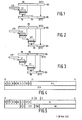
- the first method (segmentation) is illustrated in Figure 1.
- This first method divides the virtual address space (100) into segments that are continuous in memory.
- a virtual address is then composed of a segment number (SN) and an offset (OFFS).
- the MAC is always provided with a number of segment tables.
- a first part of the segment number indicates a segment table pointer (STP) which on its turn indicates a selected segment table wherein segment descriptors are stored.
- STP segment table pointer
- Those segment descriptors contain the base address of the segment in physical memory as well as the length of the segment.
- the physical address which has to be generated in order to access a location in the main memory is generated as given hereunder.
- a second part of the segment number (SN) of the virtual address indicates a location in the selected segment table (ST).
- segment descriptor At that indicated location in the segment table there is stored a segment descriptor.
- the segment length which is present in that descriptor- is compared with the offset (OFFS) of the virtual address in order to check if the offset does not exceed the segment length. If this should be the case an interrupt is generated. If on the other hand the segment length is compatible with the local memory capacity, the offset is added to the segment basis (SN + PN) present in the descriptor and the physical address (105) is herewith generated.
- the advantage of segmentation is that the designer can choose a maximum length for a segment because the segment length can be adapted to the length of the program or data to be loaded.
- the second method called two-level paging, is illustrated in Figure 2.
- the virtual address space (100) is divided into pages of fixed sizes, with each page configured to be for example 1K, 2K, 4K or 8K bytes long.
- Paging partitions physical main memory into same-sized page frames and secondary memory (e.g. the system disk) into pages.
- the paging mechanism transfers pages from secondary memory to page frames in main memory when necessary and, given a logical address, it performs the mapping operation, i.e. determining which page a logical address refers to and finding the associated page frame.
- a virtual address (100) comprises a page number PN and an offset (OFFS).
- the page number is viewed in two parts.
- a first part indicates a page table pointer (PTP) which on its turn indexes a first level page table (FPT).
- the first level page table FPT contains descriptors, each of which consists of a page table length field and a pointer.
- a few bits of the first part of the page number indicates a descriptor within the first level page table.
- the pointer of that descriptor points to a second level page table (SPT).
- a second part of the page number is used as an index into that indicated second level page table (SPT).
- the second level page table contains the page descriptors.
- a page descriptor contains attribute fields for protection codes, action codes, history information, and the physical address of the page frame.
- the final physical address (105) is formed by the concatenation of the page frame number (PB) with the offset (OFFS) field of the virtual address.
- the advantage of paging is that the pages have a fixed length which implies that when a page is removed and replaced by another one, the accessible memory space will again be completely occupied.
- the third method called segmentation with paging, is illustrated in Figure 3.
- the virtual address space (100) is divided into segments, but unlike the first method, the segments are not contiguous. Instead the pages can be scattered throughout the memory.
- Each of the segments is divided into a number of pages which have a fixed length. This method thus combines the advantages of the first and the second method.
- the virtual address is broken up into three fields: the segment number (SN), the page number (PN), and the offset (OFFS).
- the fields are not contiguous but scattered throughout the memory.
- Each segment is divided into a number of pages which have a fixed length.
- the MAC is provided with segment table memories wherein segment descriptors are stored, even as with page table memories wherein page descriptors are stored.
- the physical address which has to be generated in order to access a location in the memory is generated as given hereunder.
- the segment number (SN) or at least a part of it is used to address a segment table pointer (STP) which points to a segment table register (ST).
- STP segment table pointer
- ST segment table register
- a location in that pointed segment table is indexed by a part of the segment number in order to obtain the associated segment descriptor.
- Each of the segment descriptors indexes a page table wherein the page descriptors of the different pages of that segment are stored.
- the page number is then used as an index into the page table (PT) pointed to by the segment descriptor.
- the page descriptor is then obtained which contains the physical frame address (NB). This address when concatenated with the offset (OFFS) yields the desired physical address (105).
- the segment descriptors respectively the page descriptors are stored in the segment table (ST) respectively the page table (PT; FPT, SPT).
- Figure 4 shows an example of the format of a 32-bits segment descriptor in the segment table for a paged (non-contiguous) segment
- Figure 5 shows an example of the format of a segment descriptor for a contiguous segment.
- a segment descriptor as illustrated in Figure 4 comprises three fields:
- This (32-bit) field contains the pointer to the page table which defines the current segment.
- This (22-bit) field contains the page number of the last page in the segment. The number of pages then represents a parameter indicating the capacity of the segment.
- This field contains the attribute bits which define the status of the segment. Each use of segment may be protected differently depending on the permissions granted to the process accessing this segment.
- This field comprises for example 10 bits which have the following signification:
- This bit is used to indicate whether the segment is valid or not.
- the associated segment may not be brought into the cache memory. If the associated segment comprises semaphores or could be used by two processors or 1/0 units concurrently it should be so marked.
- This bit is usable by the software of the system. If this bit is set, a trap will be generated the first time the associated segment is accessed. Subsequent accesses to the segment may or may not generate a trap. Thus, the trap handling software should either reset this bit after the first interrupt, or should be capable of handling multiple traps. This bit is meant to provide a software filter for entry into segments.
- This bit is used to denote whether pages of a segment start at the top or bottom of the segment's virtual address space.
- the segment descriptors have a acccess permission.
- a segment may have a read (R) permission, write (W) permission, or (E) execute permission.
- R read
- W write
- E execute permission
- a read only segment would only have its R bit set, while a read/write segment would have both R and W bits set.
- Accessing a segment without proper permission causes what is termed an access violation.
- the MAC in this case causes a bus error (BERR), so that the operating system (OS) can decide what should be done.
- BERR bus error
- S segment descriptor supervisor
- the translation look-aside buffer of the MAC is provided with a memory wherein there are stored physical addresses obtained by translation. That memory is realized as a CAM (Content Addressable Memory).
- CAM Content Addressable Memory
- the present invention is addressed to the following problem which arises in such a system. It is often necessary, especially in a memory management unit, to determine whether an action at a given physical address is allowable. Stated otherwise, upon receipt by the MAC of an incoming signal (virtual address + action) from a processor which seeks to address a word in memory, the set of attributes annex to the physical address obtained by translation of the virtual address has to be compared with the action bits of the incoming signal. In effect, many conditions have to be checked at once. In particular, some of the attributes may affect whether the action required is even allowed.
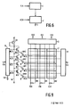
- FIG. 6 gives an example of a prior art solution of this problem.
- the virtual address (VA) is supplied to an address CAM(1), which thereupon (when present) outputs the physical address and the attributes associated with that physical address.
- the outputted attributes are presented to a comparator 2 to which there is also presented the action bits supplied by the processor together with the virtual address.
- the comparator (2) the attributes are then compared with the action and if they correspond a match signal is supplied on line 3, if not then a miss signal is supplied.
- a further memory within the translation look-aside buffer.
- That further memory is also preferably a CAM, called attribute CAM.
- attribute CAM which has a capacity for storing as many words as the address CAM, there is stored for each physical address of the address CAM its associated attribute bits.
- the virtual address is supplied to the address CAM and the action bits are supplied to the attribute CAM. Both operations are done in parallel.
- a CAM memory is built of CAM cells, each of which consits of a RAM cell (RC) plus a comparator (COM), as shown in Figure 7.
- the comparator performs the exclusive OR function on the data stored in the RAM cell and the data being present on the data lines D and DB.
- the output of the compator is the match signal that is active when the stored data matches the current input signal.
- the matched signals of all cells of the same memory word logically are tied together, forming the match line. When this line is active, the stored memory word matches the data word present on the data lines.
- Figure 8 shows an example of a CAM containing four words of three bits each. CAMs can be write/compare only or read/write/compare.
- the standard NMOS CAM cell of Figure 7 contains a logical 0 when QL is on and QR is off. The reverse occurs for a logical 1.
- the threshold voltage V TE of QCL, QCR and QCO is typically around 1 volt.
- N words of attributes stored in a CAM With N words of attributes stored in a CAM, incoming signals are compared with all of them simultaneously, causing N match lines to show the comparison results. Selection of the word to be compared with the input data can take place before, during or after the actual comparison is done by applying a current to the match line belonging to the row to be selected. This selection will only cause the selected comparison results to be shown at the output.
- Figure 9 shows a first embodiment of a translation match unit which is part of the MAC.
- the address CAM (10) receives the virtual address (VA) and generates when present the physical address (PA).
- the match lines ML01, ML11, ML21 and ML31 of the address CAM are respectively connected to a first electrode of the transistors QSO, QS1, QS2 and QS3.
- the attribute CAM (12) receives the attribute bits as supplied by the processor via the lines DOO, D10 and D20 and via the lines DBO, DB1 and DB2 their respective inverses.
- the worldline select unit 11 selects upon a received virtual address a row within the attribute CAM. In that selected row there are present the attributes of the physical address obtained by translation of the received virtual address.
- the match lines ML02, ML12, ML22 and ML32 of this attribute CAM are respectively connected to a first electrode of the transistors QMO, QM1, QM2 and QM3.
- Each of the transistors QSO, QS1, QS2 and QS3 have a second electrode connected to a match result line 14 and a third electrode connected to a second electrode of a respective transistor QMO, QM1, QM2 and QM3.
- the third electrodes of the transistors QMO, QM1, QM2 and QM3 are grounded. All QM and QS transistors are preferably enhancement transistors, while transistor QD is a deplacement transistor which is used as a switch for applying a current to the match result line 14.
- the translation match unit chooses upon a presented virtual address a word stored in one of the rows of both CAM' S .
- the selected word in the attribute CAM is compared with the action word supplied by the processor on lines D00 through D20 and DBO, DB1, DB2 and presents the results of the comparison on the match result line. Assume for example the word 2 is the chosen word.
- the address CAM supplies zeroes to the gates of QSO, QS1 and QS3 to keep them off. This isolates the match result line from QMO, QM1 and QM3. As a consequence, the conditions on match lines ML01, ML12 and ML32 do not affect the match result.
- the match select line ML21 supplies a logic 1 to the gate of QS2 to turn it on. If word 2 matches the incoming word, QCO in each cell of word 2 is off. This places match line ML22 at logic 1, consequently QM2 turns on. QS2 and QM2 then provide a path for pulling the match result line (14) to 0 to indicate a match with selected word 2. If word 2 present in the attribute CAM (12) does not match the incoming word, QCO and at least one cell of word 2 is on. ML22 goes to a 0 to turn off QM2. The match result is a logic 1 which represents a MISS.
- An action bit is considered DON'T CARE when the comparison result is not relevant in view of the comparison result of one or more other attribute bits of the action word supplied by the processor, which other attribute bit(s) have a more dominant contribution to the comparison result.
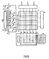
- the proposed solution of the present invention is shown in Figure 10.
- the translation-match unit shown in Figure 10 comprises an address CAM 32 and an attribute CAM 33.
- the processor supplies virtual addresses to the translation match unit. When the supplied virtual address is present in the address CAM 32, it is translated into a physical address and a MATCH signal is supplied to one of the match lines ML1.
- the attribute CAM stores the first attribute words for the different physical addresses stored in the address CAM.
- the first attribute word annex to the selected physical address is selected by means of the row select unit 36.
- the compare signal input of the attribute CAM (33) is connected to an output of a encoder (31).
- An input of the encoder (31) is connected to an output of a register 30 to which an action word, as supplied by the processor annex to a virtual address, is presented.
- the virtual address and his annexed action word are supplied in parallel to the translation match unit.
- the match result of the attribute CAM is presented on the match lines ML2.
- the match lines ML1 and ML2 are respectively connected to a match result circuit 34 which outputs a match result on match result line 35.
- An action word presented by the processor to register 30 is first encoded by the encoder (31) in order to form a second attribute word. That second attribute word is used to access attribute CAM (33).
- the PLA encoder 31 is for example formed by a ROM when the encoding of the action bits is fixed. A supplied action then forms an address for addressing a stored encoded action word.
- the PLA encoder is for example formed by an EPROM, a PLA, or an EEPROM, which gives the possibility to program the encoding of the action bits.
Landscapes
- Engineering & Computer Science (AREA)
- Theoretical Computer Science (AREA)
- Physics & Mathematics (AREA)
- General Engineering & Computer Science (AREA)
- General Physics & Mathematics (AREA)
- Computer Security & Cryptography (AREA)
- Memory System Of A Hierarchy Structure (AREA)
- Storage Device Security (AREA)
Applications Claiming Priority (2)
| Application Number | Priority Date | Filing Date | Title |
|---|---|---|---|
| US68454784A | 1984-12-21 | 1984-12-21 | |
| US684547 | 1984-12-21 |
Publications (1)
| Publication Number | Publication Date |
|---|---|
| EP0186230A2 true EP0186230A2 (de) | 1986-07-02 |
Family
ID=24748506
Family Applications (1)
| Application Number | Title | Priority Date | Filing Date |
|---|---|---|---|
| EP85201952A Withdrawn EP0186230A2 (de) | 1984-12-21 | 1985-11-26 | Speicherzugriffsteuereinheit mit paralleler Prüfung von virtueller Adresse und Aktionswort |
Country Status (2)
| Country | Link |
|---|---|
| EP (1) | EP0186230A2 (de) |
| JP (1) | JPS61156347A (de) |
Cited By (6)
| Publication number | Priority date | Publication date | Assignee | Title |
|---|---|---|---|---|
| EP1637960A3 (de) * | 2004-08-27 | 2006-11-29 | Microsoft Corporation | System und Verfahren um Adressenbits um Sicherheitseigenschaften von Daten in Adressraum zu zeigen zu verwenden |
| US7334131B2 (en) * | 2001-06-11 | 2008-02-19 | Stmicroelectronics S.A. | Protected storage of a datum in an integrated circuit |
| US7653802B2 (en) | 2004-08-27 | 2010-01-26 | Microsoft Corporation | System and method for using address lines to control memory usage |
| US7734926B2 (en) | 2004-08-27 | 2010-06-08 | Microsoft Corporation | System and method for applying security to memory reads and writes |
| US7822993B2 (en) | 2004-08-27 | 2010-10-26 | Microsoft Corporation | System and method for using address bits to affect encryption |
| US7827413B2 (en) | 2001-04-04 | 2010-11-02 | Stmicroelectronics S.A. | Extraction of a private datum to authenticate an integrated circuit |
Families Citing this family (4)
| Publication number | Priority date | Publication date | Assignee | Title |
|---|---|---|---|---|
| JPS63170778A (ja) * | 1987-01-09 | 1988-07-14 | Hitachi Ltd | 画像編集システム |
| JP2728434B2 (ja) * | 1987-06-22 | 1998-03-18 | 株式会社日立製作所 | アドレス変換装置 |
| JPH035854A (ja) * | 1989-06-01 | 1991-01-11 | Matsushita Electric Ind Co Ltd | アドレス変換装置及びアドレス変換装置における例外検出方式 |
| JP2628796B2 (ja) * | 1991-03-01 | 1997-07-09 | 住友電気工業株式会社 | スローアウェイ式エンドミル |
-
1985
- 1985-11-26 EP EP85201952A patent/EP0186230A2/de not_active Withdrawn
- 1985-12-18 JP JP60285404A patent/JPS61156347A/ja active Pending
Cited By (8)
| Publication number | Priority date | Publication date | Assignee | Title |
|---|---|---|---|---|
| US7827413B2 (en) | 2001-04-04 | 2010-11-02 | Stmicroelectronics S.A. | Extraction of a private datum to authenticate an integrated circuit |
| US7334131B2 (en) * | 2001-06-11 | 2008-02-19 | Stmicroelectronics S.A. | Protected storage of a datum in an integrated circuit |
| US7945791B2 (en) | 2001-06-11 | 2011-05-17 | Stmicroelectronics S.A. | Protected storage of a datum in an integrated circuit |
| EP1637960A3 (de) * | 2004-08-27 | 2006-11-29 | Microsoft Corporation | System und Verfahren um Adressenbits um Sicherheitseigenschaften von Daten in Adressraum zu zeigen zu verwenden |
| US7444523B2 (en) | 2004-08-27 | 2008-10-28 | Microsoft Corporation | System and method for using address bits to signal security attributes of data in the address space |
| US7653802B2 (en) | 2004-08-27 | 2010-01-26 | Microsoft Corporation | System and method for using address lines to control memory usage |
| US7734926B2 (en) | 2004-08-27 | 2010-06-08 | Microsoft Corporation | System and method for applying security to memory reads and writes |
| US7822993B2 (en) | 2004-08-27 | 2010-10-26 | Microsoft Corporation | System and method for using address bits to affect encryption |
Also Published As
| Publication number | Publication date |
|---|---|
| JPS61156347A (ja) | 1986-07-16 |
Similar Documents
| Publication | Publication Date | Title |
|---|---|---|
| US5321836A (en) | Virtual memory management method and apparatus utilizing separate and independent segmentation and paging mechanism | |
| EP0979456B1 (de) | Speicherzugangsschutz | |
| US4532606A (en) | Content addressable memory cell with shift capability | |
| US4197580A (en) | Data processing system including a cache memory | |
| CA2022656C (en) | Translation look-aside buffer for a computer memory system | |
| US6381668B1 (en) | Address mapping for system memory | |
| US4386402A (en) | Computer with dual vat buffers for accessing a common memory shared by a cache and a processor interrupt stack | |
| US4831522A (en) | Circuit and method for page addressing read only memory | |
| US5717885A (en) | TLB organization with variable page size mapping and victim-caching | |
| EP0132129A2 (de) | Adressumsetzungspuffer | |
| EP0810527A1 (de) | Sektorbasiertes virtuelles Speicherverwaltungssystem und Adressenübersetzungspufferspeicher (TLB) dafür | |
| US5790979A (en) | Translation method in which page-table progression is dynamically determined by guard-bit sequences | |
| JPH0622000B2 (ja) | マイクロプロセツサ装置 | |
| US5173872A (en) | Content addressable memory for microprocessor system | |
| JPH0769868B2 (ja) | 高速アドレス変換装置 | |
| US4580217A (en) | High speed memory management system and method | |
| US5712998A (en) | Fast fully associative translation lookaside buffer with the ability to store and manage information pertaining to at least two different page sizes | |
| US7343469B1 (en) | Remapping I/O device addresses into high memory using GART | |
| EP0602807A2 (de) | Cachespeichersystem | |
| JPH0661066B2 (ja) | 記憶制御装置 | |
| US5913222A (en) | Color correction method in a virtually addressed and physically indexed cache memory in the event of no cache hit | |
| US5220526A (en) | Method and apparatus for indicating a duplication of entries in a content addressable storage device | |
| JPS61156347A (ja) | 仮想アドレス及びアクシヨンワードを並列にチエツクするメモリアクセス制御装置 | |
| US5860145A (en) | Address translation device storage last address translation in register separate from TLB | |
| EP0175398A2 (de) | Datenverarbeitungsanordnung mit einem Speicherzugriffssteuergerät welches zur Kombination von Deskriptor-Bits aus verschiedenen mit virtuellen Adressen verbundenen Deskriptoren vorgesehen ist |
Legal Events
| Date | Code | Title | Description |
|---|---|---|---|
| PUAI | Public reference made under article 153(3) epc to a published international application that has entered the european phase |
Free format text: ORIGINAL CODE: 0009012 |
|
| AK | Designated contracting states |
Kind code of ref document: A2 Designated state(s): DE FR GB IT |
|
| STAA | Information on the status of an ep patent application or granted ep patent |
Free format text: STATUS: THE APPLICATION IS DEEMED TO BE WITHDRAWN |
|
| 18D | Application deemed to be withdrawn |
Effective date: 19890601 |
|
| RIN1 | Information on inventor provided before grant (corrected) |
Inventor name: HAGE, CORNELIS GOYERT Inventor name: KAPLINSKY, CECIL HERTZ |