EP0187475A2 - Procédé de fabrication de dispositifs semi-conducteurs ayant une couche de silicium polycristalline contenant de l'oxygène - Google Patents
Procédé de fabrication de dispositifs semi-conducteurs ayant une couche de silicium polycristalline contenant de l'oxygène Download PDFInfo
- Publication number
- EP0187475A2 EP0187475A2 EP85308845A EP85308845A EP0187475A2 EP 0187475 A2 EP0187475 A2 EP 0187475A2 EP 85308845 A EP85308845 A EP 85308845A EP 85308845 A EP85308845 A EP 85308845A EP 0187475 A2 EP0187475 A2 EP 0187475A2
- Authority
- EP
- European Patent Office
- Prior art keywords
- layer
- polycrystalline
- polycrystalline silicon
- silicon layer
- oxygen
- Prior art date
- Legal status (The legal status is an assumption and is not a legal conclusion. Google has not performed a legal analysis and makes no representation as to the accuracy of the status listed.)
- Granted
Links
Images


Classifications
-
- H—ELECTRICITY
- H10—SEMICONDUCTOR DEVICES; ELECTRIC SOLID-STATE DEVICES NOT OTHERWISE PROVIDED FOR
- H10B—ELECTRONIC MEMORY DEVICES
- H10B10/00—Static random access memory [SRAM] devices
- H10B10/15—Static random access memory [SRAM] devices comprising a resistor load element
-
- H—ELECTRICITY
- H10—SEMICONDUCTOR DEVICES; ELECTRIC SOLID-STATE DEVICES NOT OTHERWISE PROVIDED FOR
- H10B—ELECTRONIC MEMORY DEVICES
- H10B10/00—Static random access memory [SRAM] devices
-
- H—ELECTRICITY
- H10—SEMICONDUCTOR DEVICES; ELECTRIC SOLID-STATE DEVICES NOT OTHERWISE PROVIDED FOR
- H10D—INORGANIC ELECTRIC SEMICONDUCTOR DEVICES
- H10D1/00—Resistors, capacitors or inductors
- H10D1/40—Resistors
- H10D1/47—Resistors having no potential barriers
-
- H—ELECTRICITY
- H10—SEMICONDUCTOR DEVICES; ELECTRIC SOLID-STATE DEVICES NOT OTHERWISE PROVIDED FOR
- H10P—GENERIC PROCESSES OR APPARATUS FOR THE MANUFACTURE OR TREATMENT OF DEVICES COVERED BY CLASS H10
- H10P95/00—Generic processes or apparatus for manufacture or treatments not covered by the other groups of this subclass
- H10P95/90—Thermal treatments, e.g. annealing or sintering
-
- Y—GENERAL TAGGING OF NEW TECHNOLOGICAL DEVELOPMENTS; GENERAL TAGGING OF CROSS-SECTIONAL TECHNOLOGIES SPANNING OVER SEVERAL SECTIONS OF THE IPC; TECHNICAL SUBJECTS COVERED BY FORMER USPC CROSS-REFERENCE ART COLLECTIONS [XRACs] AND DIGESTS
- Y10—TECHNICAL SUBJECTS COVERED BY FORMER USPC
- Y10S—TECHNICAL SUBJECTS COVERED BY FORMER USPC CROSS-REFERENCE ART COLLECTIONS [XRACs] AND DIGESTS
- Y10S257/00—Active solid-state devices, e.g. transistors, solid-state diodes
- Y10S257/903—FET configuration adapted for use as static memory cell
- Y10S257/904—FET configuration adapted for use as static memory cell with passive components,, e.g. polysilicon resistors
Definitions
- This invention relates to methods of manufacturing semiconductor devices.
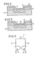
- FIG. 3 of the accompanying drawings shows a circuit diagram of a resistor load-type static random access memory (SRAM) in the form of a semiconductor device having a semiconductor substrate with a resistor electrically connected to the substrate, and including field effect transistors (FETs) 12 and resistors 13.
- SRAM static random access memory
- FIG. 1 of the accompanying drawings shows a sectional view of a first previously-proposed example of the SRAM 11.
- an SiO Z layer 15 is formed on an Si substrate 14.
- a diffusion region 17 is formed in the substrate 14 by diffusion through an opening 16 formed in the SiO Z layer 15.
- the diffusion region 17 acts as the drain for the FET 12.
- a polycrystalline Si layer 18 is formed to cover the diffusion region 17 and the SiO 2 layer 15.
- the polycrystalline Si layer 18 acts as the resistor 13.
- the stand-by current of the SRAM 11 is determined by the resistance of the resistor 13.
- the polycrystalline Si layer 18 serving as the resistor 13 has a relatively low resistivity of 5 x 10 5 ohm.cm. Therefore, the stand-by current of the SRAM 11 is relatively high, and power consumption is high. These problems become particularly noticeable when a number of SRAMs 11 are integrated.
- FIG. 2 of the accompanying drawings shows a second previously-proposed example of the SRAM 11, forming an improvement over the first example.
- the SRAM 11 of this example is substantially the same as that of the first example except that a polycrystalline Si layer 19 containing oxygen is used in place of the pure polycrystalline Si layer 18.
- polycrystalline Si containing oxygen has a very high resistivity: about 2 x 10 6 ohm.cm at an oxygen content of 2%, and about 10 10 ohm.cm at an oxygen content of 20%.
- a semiconductor device having a layer of polycrystalline Si containing oxygen formed on a semiconductor substrate is also described in issued Japanese Patent No. 53/2552.
- the polycrystalline Si layer 19 containing oxygen is formed by a low-pressure chemical vapour deposition (CVD) method using, for example, SiH 4 (flow rate: 50 cc/min), N 2 0 (flow rate: 2 cc/min), and N2 or He as needed.
- CVD chemical vapour deposition
- the SiO 2 layer 20 becomes PSG or AsSG. Even if annealing is performed after the polycrystalline Si layer 19 has been formed, the SiO 2 layer 20 remains unchanged. Therefore, it is very difficult ohmically to connect the diffusion region 17 and the polycrystalline Si layer 19.
- a method of manufacturing a semiconductor device comprising the steps of:
- an oxide formed between the first and second polycrystalline silicon layers upon formation of the second polycrystalline silicon layer containing oxygen is dispersed over the first and second polycrystalline silicon layers, thereby ohmically connecting the electrically connecting portion of the semiconductor substrate and the second polycrystalline silicon layer.
- a high resistance can be obtained in the second polycrystalline silicon layer.
- an SiO 2 layer 15 is formed on an Si substrate 14.
- a diffusion region 17 is formed in the substrate 14 by diffusion through an opening 16 formed in the SiO 2 layer 15.
- a polycrystalline Si layer 18 having a thickness of 50 to 200 angstroms (10 -10 m) is formed by a low-pressure CVD method on the diffusion region 17 and the SiO 2 layer 15. Since a gas containing oxygen is not used in this step, an SiO 2 layer is not formed between the diffusion region 17 and the polycrystalline Si layer 18.
- a polycrystalline Si layer 19 containing 2 to 10 atomic % of oxygen and having a thickness of 1,500 to 4,000 angstroms (10 -10 m) is then formed by a low-pressure CVD method on the polycrystalline Si layer 18.
- the polycrystalline Si layer 18 is oxidized, and an SiO 2 layer 20 having a thickness of about 10 to 30 angstroms (10 -10 m) is formed between the first and second Si layers 18 and 19.
- P or As ions 21 are ion-implanted in the connecting portion at a dose of 1 x 1016cm 2 and an acceleration energy of 70 keV.
- the Si substrate 14 on which the polycrystalline Si layers 18 and 19 are formed is annealed in an N 2 atmosphere at 900 to 1,000°C for 20 to 60 minutes. Then, as shown in Figure 4E, the Si crystal grains of the polycrystalline Si layers 18 and 19, which had sizes of 20 to 50 angstroms (10 -10 m), grow into Si crystal grains 22 having sizes of about 200 angstroms 5 (10" m).
- the Si0 2 layer 20, which was sandwiched between the polycrystalline Si layers 18 and 19, is formed into SiO 2 masses 23 that are dispersed between the Si crystal grains 22.
- the SiO 2 layer 20 disappears.
- the polycrystalline Si layers 18 and 19 are ohmically connected and thus the polycrystalline Si layer 19 and the diffusion region 17 are also ohmically connected.
- a resistor 13 having a resistance several times to several hundred times that of the example of Figure 1, using only the polycrystalline Si layer 18, can be formed.
- the stand-by current can be reduced to from 1/n to 11100n (where n is a positive integer smaller than 10).
- the SiO Z layer does not remain as in the case of the example of Figure 2. Therefore, the resistor 13 and the drain of the FET 12 can be ohmically connected.
- FIG 5 shows the second method embodying the invention and corresponds to Figure 4E of the first method.
- the second method has substantially the same steps as those of the first method except that the polycrystalline Si layer 18 is formed not on the entire surfaces of the diffusion region 17 and the SiO 2 layer 15, but only on the diffusion region 17 and the portion of the 5i0 2 layer 15 near the diffusion region 17.
- the polycrystalline Si layer 19 is used as a resistor in a direction along the surface of the Si substrate 14.
- a current also flows in the polycrystalline Si layer 18.
- the polycrystalline Si layer 18 Since the polycrystalline Si layer 18 has a lower resistivity than that of the polycrystalline Si layer 19, the polycrystalline Si layer 18 must be made extremely thin as compared with the polycrystalline Si layer 19 in order to obtain a high overall resistance. However, it is not easy to form a very thin polycrystalline Si layer 18, and product reliability also suffers when such a thin layer is used.
- the polycrystalline Si layer 18 can be formed to have a thickness of 1,000 to 2,000 angstroms (10 -10 m) larger than in the first method, the polycrystalline Si layer 18 can be formed easily and product reliability is improved.
- the present invention is applied to the manufacture of SRAMs.
- the invention can also be applied to the manufacture of devices other than SRAMs.
Landscapes
- Semiconductor Integrated Circuits (AREA)
- Semiconductor Memories (AREA)
Applications Claiming Priority (2)
| Application Number | Priority Date | Filing Date | Title |
|---|---|---|---|
| JP256274/84 | 1984-12-04 | ||
| JP59256274A JPS61134055A (ja) | 1984-12-04 | 1984-12-04 | 半導体装置の製造方法 |
Publications (3)
| Publication Number | Publication Date |
|---|---|
| EP0187475A2 true EP0187475A2 (fr) | 1986-07-16 |
| EP0187475A3 EP0187475A3 (en) | 1988-09-07 |
| EP0187475B1 EP0187475B1 (fr) | 1991-02-27 |
Family
ID=17290366
Family Applications (1)
| Application Number | Title | Priority Date | Filing Date |
|---|---|---|---|
| EP85308845A Expired - Lifetime EP0187475B1 (fr) | 1984-12-04 | 1985-12-04 | Procédé de fabrication de dispositifs semi-conducteurs ayant une couche de silicium polycristalline contenant de l'oxygène |
Country Status (8)
| Country | Link |
|---|---|
| US (1) | US4702937A (fr) |
| EP (1) | EP0187475B1 (fr) |
| JP (1) | JPS61134055A (fr) |
| KR (1) | KR940007539B1 (fr) |
| CN (1) | CN1005802B (fr) |
| AU (1) | AU595169B2 (fr) |
| CA (1) | CA1262522A (fr) |
| DE (1) | DE3581919D1 (fr) |
Cited By (3)
| Publication number | Priority date | Publication date | Assignee | Title |
|---|---|---|---|---|
| FR2587837A1 (fr) * | 1985-09-21 | 1987-03-27 | Stc Plc | Procede de fabrication de transistors bipolaires |
| GB2207809A (en) * | 1987-07-31 | 1989-02-08 | Samsung Semiconductor Tele | Method of manufacturing high resistance polycrystalline silicon |
| EP0339741A3 (fr) * | 1988-04-28 | 1991-03-27 | ENVEC Mess- und Regeltechnik GmbH + Co. | Procédé pour la fabrication d'une couche de résistance semiconductrice polycristalline de silicium sur un substrat en silicium |
Families Citing this family (17)
| Publication number | Priority date | Publication date | Assignee | Title |
|---|---|---|---|---|
| KR970003903B1 (en) * | 1987-04-24 | 1997-03-22 | Hitachi Mfg Kk | Semiconductor device and fabricating method thereof |
| JPH01143252A (ja) * | 1987-11-27 | 1989-06-05 | Nec Corp | 半導体装置 |
| JPH0727980B2 (ja) * | 1988-07-19 | 1995-03-29 | 三菱電機株式会社 | 高抵抗層を有する半導体装置 |
| US4954927A (en) * | 1988-09-16 | 1990-09-04 | Samsung Electronics Co., Ltd. | Double capacitor and manufacturing method thereof |
| US5037766A (en) * | 1988-12-06 | 1991-08-06 | Industrial Technology Research Institute | Method of fabricating a thin film polysilicon thin film transistor or resistor |
| US5024972A (en) * | 1990-01-29 | 1991-06-18 | Motorola, Inc. | Deposition of a conductive layer for contacts |
| US5460983A (en) * | 1993-07-30 | 1995-10-24 | Sgs-Thomson Microelectronics, Inc. | Method for forming isolated intra-polycrystalline silicon structures |
| US5470779A (en) * | 1994-07-25 | 1995-11-28 | Taiwan Semiconductor Manufacturing Company Ltd. | Method of manufacture of SRAM with SIPOS resistor |
| US5665629A (en) * | 1995-08-11 | 1997-09-09 | International Business Machines Corporation | Four transistor SRAM process |
| US5578854A (en) * | 1995-08-11 | 1996-11-26 | International Business Machines Corporation | Vertical load resistor SRAM cell |
| US6008082A (en) | 1995-09-14 | 1999-12-28 | Micron Technology, Inc. | Method of making a resistor, method of making a diode, and SRAM circuitry and other integrated circuitry |
| US5567644A (en) | 1995-09-14 | 1996-10-22 | Micron Technology, Inc. | Method of making a resistor |
| JPH09148529A (ja) * | 1995-11-24 | 1997-06-06 | Yamaha Corp | 抵抗形成法 |
| US6489213B1 (en) * | 1996-01-05 | 2002-12-03 | Integrated Device Technology, Inc. | Method for manufacturing semiconductor device containing a silicon-rich layer |
| JP3253552B2 (ja) * | 1996-05-31 | 2002-02-04 | 三洋電機株式会社 | 半導体装置の製造方法 |
| CN105336575B (zh) * | 2014-08-11 | 2018-05-25 | 中芯国际集成电路制造(上海)有限公司 | 形成多晶硅电阻的方法及半导体器件 |
| CN105390396B (zh) * | 2015-10-27 | 2018-06-08 | 株洲南车时代电气股份有限公司 | 基于igbt的分步淀积半绝缘多晶硅方法及igbt终端结构 |
Family Cites Families (4)
| Publication number | Priority date | Publication date | Assignee | Title |
|---|---|---|---|---|
| US4087571A (en) * | 1971-05-28 | 1978-05-02 | Fairchild Camera And Instrument Corporation | Controlled temperature polycrystalline silicon nucleation |
| JPS5513426B2 (fr) * | 1974-06-18 | 1980-04-09 | ||
| JPS5640269A (en) * | 1979-09-11 | 1981-04-16 | Toshiba Corp | Preparation of semiconductor device |
| US4489103A (en) * | 1983-09-16 | 1984-12-18 | Rca Corporation | SIPOS Deposition method |
-
1984
- 1984-12-04 JP JP59256274A patent/JPS61134055A/ja active Pending
-
1985
- 1985-11-04 KR KR1019850008201A patent/KR940007539B1/ko not_active Expired - Fee Related
- 1985-12-03 AU AU50722/85A patent/AU595169B2/en not_active Ceased
- 1985-12-03 CA CA000496735A patent/CA1262522A/fr not_active Expired
- 1985-12-03 US US06/804,092 patent/US4702937A/en not_active Expired - Fee Related
- 1985-12-04 DE DE8585308845T patent/DE3581919D1/de not_active Expired - Lifetime
- 1985-12-04 EP EP85308845A patent/EP0187475B1/fr not_active Expired - Lifetime
- 1985-12-04 CN CN85109507.0A patent/CN1005802B/zh not_active Expired
Cited By (5)
| Publication number | Priority date | Publication date | Assignee | Title |
|---|---|---|---|---|
| FR2587837A1 (fr) * | 1985-09-21 | 1987-03-27 | Stc Plc | Procede de fabrication de transistors bipolaires |
| GB2207809A (en) * | 1987-07-31 | 1989-02-08 | Samsung Semiconductor Tele | Method of manufacturing high resistance polycrystalline silicon |
| DE3825734A1 (de) * | 1987-07-31 | 1989-04-20 | Samsung Electronics Co Ltd | Verfahren zur herstellung von polykristallinem silizium mit hohem widerstandswert |
| GB2207809B (en) * | 1987-07-31 | 1991-04-03 | Samsung Semiconductor Tele | Method of manufacturing polycrystalline silicon |
| EP0339741A3 (fr) * | 1988-04-28 | 1991-03-27 | ENVEC Mess- und Regeltechnik GmbH + Co. | Procédé pour la fabrication d'une couche de résistance semiconductrice polycristalline de silicium sur un substrat en silicium |
Also Published As
| Publication number | Publication date |
|---|---|
| CA1262522A (fr) | 1989-10-31 |
| DE3581919D1 (de) | 1991-04-04 |
| CN85109507A (zh) | 1986-06-10 |
| CN1005802B (zh) | 1989-11-15 |
| EP0187475A3 (en) | 1988-09-07 |
| KR940007539B1 (ko) | 1994-08-19 |
| US4702937A (en) | 1987-10-27 |
| AU5072285A (en) | 1986-06-12 |
| EP0187475B1 (fr) | 1991-02-27 |
| KR860005437A (ko) | 1986-07-23 |
| JPS61134055A (ja) | 1986-06-21 |
| AU595169B2 (en) | 1990-03-29 |
Similar Documents
| Publication | Publication Date | Title |
|---|---|---|
| EP0187475B1 (fr) | Procédé de fabrication de dispositifs semi-conducteurs ayant une couche de silicium polycristalline contenant de l'oxygène | |
| US6198157B1 (en) | Semiconductor device having buried boron and carbon regions | |
| US5202574A (en) | Semiconductor having improved interlevel conductor insulation | |
| US4961103A (en) | Semiconductor device having polycrystalline silicon resistor | |
| US5861651A (en) | Field effect devices and capacitors with improved thin film dielectrics and method for making same | |
| US4717681A (en) | Method of making a heterojunction bipolar transistor with SIPOS | |
| US5459101A (en) | Method for fabricating a semiconductor device comprising a polycide structure | |
| US4356040A (en) | Semiconductor device having improved interlevel conductor insulation | |
| US5378652A (en) | Method of making a through hole in multi-layer insulating films | |
| US5187559A (en) | Semiconductor device and process for producing same | |
| US4786612A (en) | Plasma enhanced chemical vapor deposited vertical silicon nitride resistor | |
| US5278099A (en) | Method for manufacturing a semiconductor device having wiring electrodes | |
| US4704647A (en) | Magnetic recording and reproducing system with a cleaning mechanism | |
| EP0128385A2 (fr) | Procédé pour fabriquer un dispositif semi-conducteur ayant des électrodes et des interconnexions | |
| US6313728B1 (en) | Stabilized polysilicon resistor and a method of manufacturing it | |
| US4460417A (en) | Method of manufacturing insulating film and electric device utilizing the same | |
| US5291058A (en) | Semiconductor device silicon via fill formed in multiple dielectric layers | |
| JP3213909B2 (ja) | 抵抗およびその作製方法 | |
| US5705845A (en) | Semiconductor device with particular metal silicide film | |
| EP0073075B1 (fr) | Dispositif semi-conducteur comprenant du silicium polycristallin et procédé pour la fabrication du dispositif | |
| US5612236A (en) | Method of forming a silicon semiconductor device using doping during deposition of polysilicon | |
| US4380773A (en) | Self aligned aluminum polycrystalline silicon contact | |
| US5521416A (en) | Semiconductor device having gate electrode and impurity diffusion layer different in conductivity type and method of manufacturing the same | |
| US5138425A (en) | Semiconductor integrated circuit device with nitride barrier layer ion implanted with resistivity decreasing elements | |
| EP0613180A2 (fr) | Dispositif semi-conducteur comprenant des électrodes d'interconnexion. |
Legal Events
| Date | Code | Title | Description |
|---|---|---|---|
| PUAI | Public reference made under article 153(3) epc to a published international application that has entered the european phase |
Free format text: ORIGINAL CODE: 0009012 |
|
| AK | Designated contracting states |
Kind code of ref document: A2 Designated state(s): DE FR GB IT NL |
|
| PUAL | Search report despatched |
Free format text: ORIGINAL CODE: 0009013 |
|
| AK | Designated contracting states |
Kind code of ref document: A3 Designated state(s): DE FR GB IT NL |
|
| 17P | Request for examination filed |
Effective date: 19881222 |
|
| 17Q | First examination report despatched |
Effective date: 19890524 |
|
| GRAA | (expected) grant |
Free format text: ORIGINAL CODE: 0009210 |
|
| ITF | It: translation for a ep patent filed | ||
| AK | Designated contracting states |
Kind code of ref document: B1 Designated state(s): DE FR GB IT NL |
|
| PG25 | Lapsed in a contracting state [announced via postgrant information from national office to epo] |
Ref country code: NL Effective date: 19910227 |
|
| REF | Corresponds to: |
Ref document number: 3581919 Country of ref document: DE Date of ref document: 19910404 |
|
| NLV1 | Nl: lapsed or annulled due to failure to fulfill the requirements of art. 29p and 29m of the patents act | ||
| EN | Fr: translation not filed | ||
| PG25 | Lapsed in a contracting state [announced via postgrant information from national office to epo] |
Ref country code: FR Effective date: 19910719 |
|
| PG25 | Lapsed in a contracting state [announced via postgrant information from national office to epo] |
Ref country code: GB Effective date: 19911204 |
|
| PLBE | No opposition filed within time limit |
Free format text: ORIGINAL CODE: 0009261 |
|
| STAA | Information on the status of an ep patent application or granted ep patent |
Free format text: STATUS: NO OPPOSITION FILED WITHIN TIME LIMIT |
|
| 26N | No opposition filed | ||
| GBPC | Gb: european patent ceased through non-payment of renewal fee | ||
| PG25 | Lapsed in a contracting state [announced via postgrant information from national office to epo] |
Ref country code: DE Effective date: 19920901 |
|
| REG | Reference to a national code |
Ref country code: FR Ref legal event code: ST |