EP0192511A1 - Verfahren zum Herstellen einer Diode, deren Kontaktanschluss selbstausrichtend mit einem Gate ist - Google Patents
Verfahren zum Herstellen einer Diode, deren Kontaktanschluss selbstausrichtend mit einem Gate ist Download PDFInfo
- Publication number
- EP0192511A1 EP0192511A1 EP86400105A EP86400105A EP0192511A1 EP 0192511 A1 EP0192511 A1 EP 0192511A1 EP 86400105 A EP86400105 A EP 86400105A EP 86400105 A EP86400105 A EP 86400105A EP 0192511 A1 EP0192511 A1 EP 0192511A1
- Authority
- EP
- European Patent Office
- Prior art keywords
- layer
- diode
- substrate
- polycrystalline silicon
- grid
- Prior art date
- Legal status (The legal status is an assumption and is not a legal conclusion. Google has not performed a legal analysis and makes no representation as to the accuracy of the status listed.)
- Granted
Links
Images



Classifications
-
- H—ELECTRICITY
- H10—SEMICONDUCTOR DEVICES; ELECTRIC SOLID-STATE DEVICES NOT OTHERWISE PROVIDED FOR
- H10P—GENERIC PROCESSES OR APPARATUS FOR THE MANUFACTURE OR TREATMENT OF DEVICES COVERED BY CLASS H10
- H10P76/00—Manufacture or treatment of masks on semiconductor bodies, e.g. by lithography or photolithography
- H10P76/40—Manufacture or treatment of masks on semiconductor bodies, e.g. by lithography or photolithography of masks comprising inorganic materials
-
- H—ELECTRICITY
- H10—SEMICONDUCTOR DEVICES; ELECTRIC SOLID-STATE DEVICES NOT OTHERWISE PROVIDED FOR
- H10F—INORGANIC SEMICONDUCTOR DEVICES SENSITIVE TO INFRARED RADIATION, LIGHT, ELECTROMAGNETIC RADIATION OF SHORTER WAVELENGTH OR CORPUSCULAR RADIATION
- H10F39/00—Integrated devices, or assemblies of multiple devices, comprising at least one element covered by group H10F30/00, e.g. radiation detectors comprising photodiode arrays
- H10F39/10—Integrated devices
- H10F39/12—Image sensors
- H10F39/15—Charge-coupled device [CCD] image sensors
- H10F39/153—Two-dimensional or three-dimensional array CCD image sensors
-
- H—ELECTRICITY
- H10—SEMICONDUCTOR DEVICES; ELECTRIC SOLID-STATE DEVICES NOT OTHERWISE PROVIDED FOR
- H10P—GENERIC PROCESSES OR APPARATUS FOR THE MANUFACTURE OR TREATMENT OF DEVICES COVERED BY CLASS H10
- H10P95/00—Generic processes or apparatus for manufacture or treatments not covered by the other groups of this subclass
-
- H—ELECTRICITY
- H10—SEMICONDUCTOR DEVICES; ELECTRIC SOLID-STATE DEVICES NOT OTHERWISE PROVIDED FOR
- H10W—GENERIC PACKAGES, INTERCONNECTIONS, CONNECTORS OR OTHER CONSTRUCTIONAL DETAILS OF DEVICES COVERED BY CLASS H10
- H10W20/00—Interconnections in chips, wafers or substrates
- H10W20/01—Manufacture or treatment
- H10W20/031—Manufacture or treatment of conductive parts of the interconnections
- H10W20/064—Manufacture or treatment of conductive parts of the interconnections by modifying the conductivity of conductive parts, e.g. by alloying
- H10W20/065—Manufacture or treatment of conductive parts of the interconnections by modifying the conductivity of conductive parts, e.g. by alloying by making at least a portion of the conductive part non-conductive, e.g. by oxidation
-
- Y—GENERAL TAGGING OF NEW TECHNOLOGICAL DEVELOPMENTS; GENERAL TAGGING OF CROSS-SECTIONAL TECHNOLOGIES SPANNING OVER SEVERAL SECTIONS OF THE IPC; TECHNICAL SUBJECTS COVERED BY FORMER USPC CROSS-REFERENCE ART COLLECTIONS [XRACs] AND DIGESTS
- Y10—TECHNICAL SUBJECTS COVERED BY FORMER USPC
- Y10S—TECHNICAL SUBJECTS COVERED BY FORMER USPC CROSS-REFERENCE ART COLLECTIONS [XRACs] AND DIGESTS
- Y10S148/00—Metal treatment
- Y10S148/082—Ion implantation FETs/COMs
Definitions
- the present invention relates to a method for obtaining a diode whose contact point is self-aligned with a grid.
- the invention applies in particular to the making of contact points at the junctions of drains or sources of the unipolar transistors known under the designation MOS which is the abbreviation of "Metal Oxide Semiconductor" and to those of the photosensitive elements of the matrices line transfer.
- MOS Metal Oxide Semiconductor
- the diode is self-positioned with respect to the grid, but the contact must be made after the oxidation which follows the implantation of diffusion of the impurities which form the junction of the diode, therefore it is not no longer possible to precisely position the contact area with respect to the grid, there is therefore a risk of short circuit between the diode and the grid, by means of metallization.
- the object of the invention is to overcome the aforementioned drawbacks.
- the subject of the invention is a process for obtaining a diode, the contact point of which is self-aligned with a grid, characterized in that it consists in depositing on a semiconductor substrate at least a first layer of dielectric material, to deposit on the last dielectric layer a layer of polycrystalline silicon to form the grid and then a second layer of polycrystalline silicon above the first layer, to be etched in the polycrystalline silicon layers from the contact diode until the dielectric layer is exposed, to oxidize the second layer of polycrystalline silicon sufficiently so that the oxidized layer completely covers the first layer of silicon forming the grid and only covers partially the exposed part of the dielectric layer and to doping the part of the substrate not covered by the oxide layer to form the junction of the diode.
- the method according to the invention has the main advantage that it makes it possible to make an interconnection contact with a diode, of the same dimensions as the latter and self-aligned with respect to a grid by the fact that the diode, the contact and part of the grid are made with the same level of masking.
- the method according to the invention also has the advantage of eliminating a photolithography which makes it possible to improve the compactness of the products produced. It also makes it possible to reduce the depth of the diode junction, which can be formed just before the aluminum metallization of the contact points.
- the method according to the invention eliminates the risks of short-circuiting the grids with the adjacent elements.
- FIGS. 1A, 1B and 1C represent the phases of obtaining a contact diode according to a photolithography process.
- a photo-grid is first produced in the manner shown in FIG. 1A by depositing on a semiconductor substrate 1 a first layer of silica 2, then a second layer of silicon nitride 3 above of the silica layer 2, and finally to form a grid by photolitography on a conductive silicon layer 4.
- the photo-diode is then formed, as shown in FIG. 1B, by ion implantation in a zone 6 of the substrate 1, self-aligned with the grid 4 through a mask 5.
- the photo-contact is then formed in the step shown in FIG.
- the method according to the invention which is described below using FIGS. 2A to 2D, overcomes this drawback. It consists, in a first step shown in FIG. 2A, of depositing on a silicon substrate 9 a first layer 10 of silica then a second layer of silicon nitride 11 above the first layer of silica 10 and then to form by photolithography on a first deposit of polycrystalline silicon 12 the grid to be produced, then to cover the first layer of silicon 12 with a second layer of polycrystalline silicon 13.
- the layers of polycrystalline silicon 12 and 13 are etched to expose the layer of silicon nitride 11 inside a window 14 formed at the place where the diode is to be formed. Then, at the step shown in FIG.
- the silicon layer 13 is oxidized to isolate the grid formed by the polycrystalline silicon layer 12.
- the layer of silicon nitride 1 and the layer of silica 10 are attacked to expose the upper face of the substrate in the window 14 formed by the previous etching, and the diode is formed inside the window 14 by ion implantation or by diffusion of impurities in the substrate 9 inside the window 14 which has the advantage of making it possible to practice a minimum drawing time of the implanted or diffused impurities and makes it possible to obtain a lower junction depth.
- the diode may be formed with the step shown in FIG.
- the method according to the invention makes it possible to obtain an interconnection contact of the diode of the same dimensions as the diode itself, which improves the compactness of the products obtained and makes it possible in the first case to decrease the junction depth of the diode which can be formed just before the metallization operation, by aluminum, for example, contact points.
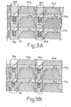
- FIG. 3A represents a line transfer matrix having diodes with contact points obtained according to the method of the known art described previously using FIGS. 1A and 1B.
- the matrix shown consists of four parts, a first part is formed by a set of storage diodes 15a to 15f representing photosensitive surface elements, a second part is formed by a set of readout diodes 16a to 16d, a third part is formed by grids 17a to 17b to control the passage of electric charges between the storage diodes and the reading diodes, and a fourth part is formed by the interconnection lines 18a 18b connected to the reading diodes for transferring, for example, loads read to an outdoor CCD reader.
- the interconnection lines are perpendicular to the control grids for the passage of charges and a thick oxide 19 isolates the photosensitive surfaces 15a to 15f from the read diodes 16a to 16d.
- the method according to the invention makes it possible to exercise control over the dimensions of the contact opening as a function of the thickness of the silicon layer 13 used.
- the contact dimension n which is obtained depends, on the one hand, on the nominal dimension m of the window made in the silicon layer 12 and on the other hand, of the thickness of the oxide formed 13.
- the greater the thickness of the oxide formed 18 the more the dimensions of the contact opening of the diodes 16a to 16d decrease and the more it is possible to increase the photosensitive surface of the storage diodes 15a to 15f. This result goes against the results obtained by traditional methods, because returning to FIG.
- the contact opening in a usual process consists in attacking the insulating layer of silicon oxide 7 through a mask M which results in obtaining an opening n shown in FIG. 5 which can only increase as a function of the thickness of the oxide layer 7 produced relative to the opening m made in the mask M.
- MOS transistor source drain contact points can be obtained using the method according to the invention, either by forming the contact diodes of the MOS transistor at the end of the process for obtaining the transistor, or by forming the diodes. before the second silicon deposit.
- the procedure is as in FIG. 2A by depositing on a semiconductor substrate 20 a first layer of silica 21 followed by a second layer of silicon nitride 22 and depositing above the layer of silicon nitride 22 a first layer of silicon 23, then a second layer of silicon 24, the latter then being transformed into oxide to form the insulator of the grid.
- the silicon layers 23 and 24 are etched as shown in FIG.
- the gate G of the transistor and two windows 25 and 26 located on either side of the gate G.
- the layer of silicon nitride 22 and the thin layer of silicon oxide 21 are removed to allow access to the substrate 20 for ion implantation of the substrate 20 through windows 25 and 26.
- the diodes are formed before the formation of the gate-connection insulating oxide. Self-alignment is then possible by protecting the silicon nitride by an excess in the grid of the future contact zone.
- the silicon layer 23 forming the grid is first of all covered with a layer of filler silicon 24 (FIG. 7B) then the filler silicon and the layer of silicon forming the grid are etched to form the window 25 ( FIG. 7C) and reveal the layer of silicon nitride 22 (FIG. 7D) so as not to have discontinuities between the diode and the contact zone which will subsequently be doped (FIG. 7E).
- the method according to the invention is also applicable to the manufacture of diodes produced while keeping the nitride-oxide double layer, according to the stages of the method represented in FIGS. 8A to 8E.
- this method after implantation (FIG. 8A) of the diode through the double layer of silica 21 and of silicon nitride 22, the filler silicon 24 is deposited above the silicon layer 23 (FIG. 8B), then the filler silicon is etched in the manner shown in FIG.
- the self-alignment can then be carried out by etching the silicon of the grid at the same time as the layer of filler silicon and after the phase of oxidation shown in Figure 8D, the junction is accessed by attacking the silicon nitride layer 22 and the thin oxide layer 21.
Landscapes
- Solid State Image Pick-Up Elements (AREA)
- Electrodes Of Semiconductors (AREA)
Applications Claiming Priority (2)
| Application Number | Priority Date | Filing Date | Title |
|---|---|---|---|
| FR8501085A FR2576710B1 (fr) | 1985-01-25 | 1985-01-25 | Procede d'obtention d'une diode dont la prise de contact est auto-alignee a une grille |
| FR8501085 | 1985-01-25 |
Publications (2)
| Publication Number | Publication Date |
|---|---|
| EP0192511A1 true EP0192511A1 (de) | 1986-08-27 |
| EP0192511B1 EP0192511B1 (de) | 1989-11-08 |
Family
ID=9315629
Family Applications (1)
| Application Number | Title | Priority Date | Filing Date |
|---|---|---|---|
| EP86400105A Expired EP0192511B1 (de) | 1985-01-25 | 1986-01-20 | Verfahren zum Herstellen einer Diode, deren Kontaktanschluss selbstausrichtend mit einem Gate ist |
Country Status (5)
| Country | Link |
|---|---|
| US (1) | US4692995A (de) |
| EP (1) | EP0192511B1 (de) |
| JP (1) | JPS61176152A (de) |
| DE (1) | DE3666898D1 (de) |
| FR (1) | FR2576710B1 (de) |
Cited By (1)
| Publication number | Priority date | Publication date | Assignee | Title |
|---|---|---|---|---|
| US7425005B2 (en) | 2003-10-24 | 2008-09-16 | Aloha, Llc | Suspensions for low floor vehicles |
Families Citing this family (4)
| Publication number | Priority date | Publication date | Assignee | Title |
|---|---|---|---|---|
| JPH0475964A (ja) * | 1990-07-13 | 1992-03-10 | Tokyo Kikai Seisakusho Ltd | 輪転機のチョッパー折り料紙規制装置 |
| FR2679379B1 (fr) * | 1991-07-16 | 1997-04-25 | Thomson Composants Militaires | Procede de fabrication de circuits integres avec electrodes tres etroites. |
| US6197649B1 (en) * | 1998-08-05 | 2001-03-06 | International Rectifier Corp. | Process for manufacturing planar fast recovery diode using reduced number of masking steps |
| US6445021B1 (en) * | 2000-09-20 | 2002-09-03 | International Business Machines Corporation | Negative differential resistance reoxidized nitride silicon-based photodiode and method |
Citations (3)
| Publication number | Priority date | Publication date | Assignee | Title |
|---|---|---|---|---|
| US4247861A (en) * | 1979-03-09 | 1981-01-27 | Rca Corporation | High performance electrically alterable read-only memory (EAROM) |
| FR2464561A1 (fr) * | 1979-08-31 | 1981-03-06 | Thomson Csf | Structure de transistors complementaires (cmos) et son procede de fabrication |
| EP0051534A2 (de) * | 1980-10-29 | 1982-05-12 | FAIRCHILD CAMERA & INSTRUMENT CORPORATION | Selbstjustierendes Verfahren zur Herstellung integrierter Stromkreisstrukturen unter Verwendung unterschiedlicher Oxydationsraten |
Family Cites Families (6)
| Publication number | Priority date | Publication date | Assignee | Title |
|---|---|---|---|---|
| US4506437A (en) * | 1978-05-26 | 1985-03-26 | Rockwell International Corporation | Process for and structure of high density VLSI circuits, having self-aligned gates and contacts for FET devices and conducting lines |
| US4477962A (en) * | 1978-05-26 | 1984-10-23 | Rockwell International Corporation | Process for and structure of high density VLSI circuits, having self-aligned gates and contacts for FET devices and conducting lines |
| US4466172A (en) * | 1979-01-08 | 1984-08-21 | American Microsystems, Inc. | Method for fabricating MOS device with self-aligned contacts |
| FR2461360A1 (fr) * | 1979-07-10 | 1981-01-30 | Thomson Csf | Procede de fabrication d'un transistor a effet de champ du type dmos a fonctionnement vertical et transistor obtenu par ce procede |
| US4305200A (en) * | 1979-11-06 | 1981-12-15 | Hewlett-Packard Company | Method of forming self-registering source, drain, and gate contacts for FET transistor structures |
| US4486943A (en) * | 1981-12-16 | 1984-12-11 | Inmos Corporation | Zero drain overlap and self aligned contact method for MOS devices |
-
1985
- 1985-01-25 FR FR8501085A patent/FR2576710B1/fr not_active Expired
-
1986
- 1986-01-20 EP EP86400105A patent/EP0192511B1/de not_active Expired
- 1986-01-20 DE DE8686400105T patent/DE3666898D1/de not_active Expired
- 1986-01-22 JP JP61011811A patent/JPS61176152A/ja active Pending
- 1986-01-24 US US06/822,028 patent/US4692995A/en not_active Expired - Fee Related
Patent Citations (3)
| Publication number | Priority date | Publication date | Assignee | Title |
|---|---|---|---|---|
| US4247861A (en) * | 1979-03-09 | 1981-01-27 | Rca Corporation | High performance electrically alterable read-only memory (EAROM) |
| FR2464561A1 (fr) * | 1979-08-31 | 1981-03-06 | Thomson Csf | Structure de transistors complementaires (cmos) et son procede de fabrication |
| EP0051534A2 (de) * | 1980-10-29 | 1982-05-12 | FAIRCHILD CAMERA & INSTRUMENT CORPORATION | Selbstjustierendes Verfahren zur Herstellung integrierter Stromkreisstrukturen unter Verwendung unterschiedlicher Oxydationsraten |
Non-Patent Citations (3)
| Title |
|---|
| IBM TECHNICAL DISCLOSURE BULLETIN, vol. 22, no. 8B, janvier 1980, pages 3688-3691, New York, US; R.C. VARSHNEY: "Polysilicon oxide process for small line gaps" * |
| IEDM INTERNATIONAL ELECTRON DEVICES MEETING, Washington, DC, 8-10 décembre 1980, Technical Digest, papier 6.3, pages 140-143, IEEE, New York, US; H.S. FU et al.: "A new MOS transistor design with self-registering source-drain and gate contacts" * |
| IEEE ELECTRON DEVICE LETTERS, vol. EDL-3, no. 2, février 1982, pages 40-42, IEEE, New York, US; S. HSIA et al.: "Polysilicon oxidation self-aligned MOS (POSA MOS) - a new self-aligned double source/drain ion implantation technique for VLSI" * |
Cited By (1)
| Publication number | Priority date | Publication date | Assignee | Title |
|---|---|---|---|---|
| US7425005B2 (en) | 2003-10-24 | 2008-09-16 | Aloha, Llc | Suspensions for low floor vehicles |
Also Published As
| Publication number | Publication date |
|---|---|
| JPS61176152A (ja) | 1986-08-07 |
| DE3666898D1 (en) | 1989-12-14 |
| EP0192511B1 (de) | 1989-11-08 |
| FR2576710A1 (fr) | 1986-08-01 |
| US4692995A (en) | 1987-09-15 |
| FR2576710B1 (fr) | 1988-03-04 |
Similar Documents
| Publication | Publication Date | Title |
|---|---|---|
| EP0258141B1 (de) | MIS integrierte Schaltung, wie eine EPROM-Speicherzelle, und Verfahren zu deren Herstellung | |
| US4613402A (en) | Method of making edge-aligned implants and electrodes therefor | |
| US5858843A (en) | Low temperature method of forming gate electrode and gate dielectric | |
| EP0038238B1 (de) | Verfahren zur Herstellung einer Halbleiteranordnung mit von der Oberfläche aus zugänglichem, tief eingebettetem Gitter | |
| US5747379A (en) | Method of fabricating seamless tungsten plug employing tungsten redeposition and etch back | |
| US5427970A (en) | Method of making flash memory with high coupling ratio | |
| FR2458902A1 (fr) | Procede pour fabriquer des circuits mos integres avec et sans transistors de memoire mnos selon la technologie des grilles en silicium | |
| EP0013342B1 (de) | Verfahren zur Herstellung selbstausrichtender Feldeffekt-Transistoren des Metallhalbleitertyps | |
| EP0299853A1 (de) | Verfahren zum Herstellen einer Speicherzelle | |
| US4746622A (en) | Process for preparing a charge coupled device with charge transfer direction biasing implants | |
| EP0022388B1 (de) | Verfahren zur Herstellung eines vertikalen Feldeffekttransistors vom DMOS-Typ | |
| FR2510819A1 (fr) | Procede de fabrication d'un composant misfet et composant misfet ainsi produit | |
| EP0003926B1 (de) | Verfahren zur Herstellung eines Feldeffekttransistors mit isolierter Gateelektrode | |
| FR2616576A1 (fr) | Cellule de memoire eprom et son procede de fabrication | |
| US4742027A (en) | Method of fabricating a charge coupled device | |
| US5492852A (en) | Method for fabricating a solid imaging device having improved smear and breakdown voltage characteristics | |
| US4656729A (en) | Dual electron injection structure and process with self-limiting oxidation barrier | |
| EP0192511B1 (de) | Verfahren zum Herstellen einer Diode, deren Kontaktanschluss selbstausrichtend mit einem Gate ist | |
| EP0190243B1 (de) | Verfahren zur herstellung einer integrierten schaltung vom mis-typ | |
| JPH10154805A (ja) | 固体撮像素子及びその製造方法 | |
| FR2583920A1 (fr) | Procede de fabrication d'un circuit integre et notamment d'une memoire eprom comportant deux composants distincts isoles electriquement | |
| EP0209425B1 (de) | Verfahren zum Herstellen einer Halbleiteranordnung mit Gates auf mehreren Niveaus | |
| FR2483685A1 (fr) | Transistor de puissance a effet de champ (fet) du type v-mos a grille maillee | |
| FR2734403A1 (fr) | Isolement plan dans des circuits integres | |
| EP0157677B2 (de) | Verfahren zur Verbindung der aktiven Bereiche und/oder der Steuerelektroden von einer CMOS-integrierten Schaltung |
Legal Events
| Date | Code | Title | Description |
|---|---|---|---|
| PUAI | Public reference made under article 153(3) epc to a published international application that has entered the european phase |
Free format text: ORIGINAL CODE: 0009012 |
|
| AK | Designated contracting states |
Kind code of ref document: A1 Designated state(s): DE GB NL |
|
| 17P | Request for examination filed |
Effective date: 19870126 |
|
| 17Q | First examination report despatched |
Effective date: 19890404 |
|
| RAP3 | Party data changed (applicant data changed or rights of an application transferred) |
Owner name: THOMSON-CSF |
|
| GRAA | (expected) grant |
Free format text: ORIGINAL CODE: 0009210 |
|
| AK | Designated contracting states |
Kind code of ref document: B1 Designated state(s): DE GB NL |
|
| REF | Corresponds to: |
Ref document number: 3666898 Country of ref document: DE Date of ref document: 19891214 |
|
| GBT | Gb: translation of ep patent filed (gb section 77(6)(a)/1977) | ||
| PLBE | No opposition filed within time limit |
Free format text: ORIGINAL CODE: 0009261 |
|
| STAA | Information on the status of an ep patent application or granted ep patent |
Free format text: STATUS: NO OPPOSITION FILED WITHIN TIME LIMIT |
|
| 26N | No opposition filed | ||
| PGFP | Annual fee paid to national office [announced via postgrant information from national office to epo] |
Ref country code: DE Payment date: 19901220 Year of fee payment: 6 |
|
| PGFP | Annual fee paid to national office [announced via postgrant information from national office to epo] |
Ref country code: GB Payment date: 19901231 Year of fee payment: 6 |
|
| PGFP | Annual fee paid to national office [announced via postgrant information from national office to epo] |
Ref country code: NL Payment date: 19910131 Year of fee payment: 6 |
|
| PG25 | Lapsed in a contracting state [announced via postgrant information from national office to epo] |
Ref country code: GB Effective date: 19920120 |
|
| PG25 | Lapsed in a contracting state [announced via postgrant information from national office to epo] |
Ref country code: NL Effective date: 19920801 |
|
| NLV4 | Nl: lapsed or anulled due to non-payment of the annual fee | ||
| REG | Reference to a national code |
Ref country code: GB Ref legal event code: PCNP |
|
| PG25 | Lapsed in a contracting state [announced via postgrant information from national office to epo] |
Ref country code: DE Effective date: 19921001 |