EP0193021A1 - Procédé pour la formation d'un dispositif comportant de l'arsénide de gallium implanté - Google Patents
Procédé pour la formation d'un dispositif comportant de l'arsénide de gallium implanté Download PDFInfo
- Publication number
- EP0193021A1 EP0193021A1 EP86101712A EP86101712A EP0193021A1 EP 0193021 A1 EP0193021 A1 EP 0193021A1 EP 86101712 A EP86101712 A EP 86101712A EP 86101712 A EP86101712 A EP 86101712A EP 0193021 A1 EP0193021 A1 EP 0193021A1
- Authority
- EP
- European Patent Office
- Prior art keywords
- silicon
- layer
- annealing
- gaas
- capping layer
- Prior art date
- Legal status (The legal status is an assumption and is not a legal conclusion. Google has not performed a legal analysis and makes no representation as to the accuracy of the status listed.)
- Withdrawn
Links
Images
Classifications
-
- H—ELECTRICITY
- H10—SEMICONDUCTOR DEVICES; ELECTRIC SOLID-STATE DEVICES NOT OTHERWISE PROVIDED FOR
- H10P—GENERIC PROCESSES OR APPARATUS FOR THE MANUFACTURE OR TREATMENT OF DEVICES COVERED BY CLASS H10
- H10P14/00—Formation of materials, e.g. in the shape of layers or pillars
- H10P14/60—Formation of materials, e.g. in the shape of layers or pillars of insulating materials
-
- H—ELECTRICITY
- H10—SEMICONDUCTOR DEVICES; ELECTRIC SOLID-STATE DEVICES NOT OTHERWISE PROVIDED FOR
- H10P—GENERIC PROCESSES OR APPARATUS FOR THE MANUFACTURE OR TREATMENT OF DEVICES COVERED BY CLASS H10
- H10P14/00—Formation of materials, e.g. in the shape of layers or pillars
- H10P14/20—Formation of materials, e.g. in the shape of layers or pillars of semiconductor materials
- H10P14/34—Deposited materials, e.g. layers
- H10P14/3402—Deposited materials, e.g. layers characterised by the chemical composition
- H10P14/3404—Deposited materials, e.g. layers characterised by the chemical composition being Group IVA materials
- H10P14/3411—Silicon, silicon germanium or germanium
-
- H—ELECTRICITY
- H10—SEMICONDUCTOR DEVICES; ELECTRIC SOLID-STATE DEVICES NOT OTHERWISE PROVIDED FOR
- H10P—GENERIC PROCESSES OR APPARATUS FOR THE MANUFACTURE OR TREATMENT OF DEVICES COVERED BY CLASS H10
- H10P95/00—Generic processes or apparatus for manufacture or treatments not covered by the other groups of this subclass
- H10P95/90—Thermal treatments, e.g. annealing or sintering
- H10P95/904—Thermal treatments, e.g. annealing or sintering of Group III-V semiconductors
-
- Y—GENERAL TAGGING OF NEW TECHNOLOGICAL DEVELOPMENTS; GENERAL TAGGING OF CROSS-SECTIONAL TECHNOLOGIES SPANNING OVER SEVERAL SECTIONS OF THE IPC; TECHNICAL SUBJECTS COVERED BY FORMER USPC CROSS-REFERENCE ART COLLECTIONS [XRACs] AND DIGESTS
- Y10—TECHNICAL SUBJECTS COVERED BY FORMER USPC
- Y10S—TECHNICAL SUBJECTS COVERED BY FORMER USPC CROSS-REFERENCE ART COLLECTIONS [XRACs] AND DIGESTS
- Y10S148/00—Metal treatment
- Y10S148/084—Ion implantation of compound devices
-
- Y—GENERAL TAGGING OF NEW TECHNOLOGICAL DEVELOPMENTS; GENERAL TAGGING OF CROSS-SECTIONAL TECHNOLOGIES SPANNING OVER SEVERAL SECTIONS OF THE IPC; TECHNICAL SUBJECTS COVERED BY FORMER USPC CROSS-REFERENCE ART COLLECTIONS [XRACs] AND DIGESTS
- Y10—TECHNICAL SUBJECTS COVERED BY FORMER USPC
- Y10S—TECHNICAL SUBJECTS COVERED BY FORMER USPC CROSS-REFERENCE ART COLLECTIONS [XRACs] AND DIGESTS
- Y10S438/00—Semiconductor device manufacturing: process
- Y10S438/902—Capping layer
Definitions
- This invention relates to a method of forming an ion implanted gallium arsenide (GaAs) device.
- doping may be accomplished by ion implantation of dopant elements such as Si, Se, Be, or Mg to a predetermined depth to provide desired electrical characteristics to the device. Subsequent to the step of ion implanting the semiconductor material, it is necessary to anneal the semiconductor material to remove the damage caused by the implanted ions.
- dopant elements such as Si, Se, Be, or Mg
- the annealing step is frequently done in the temperature range of 700-1000°C and presents difficulties due to the tendency for the GaAs to decompose incongruently with the emission of As.
- the surface of the semiconductor becomes excessively rich in Ga, and droplets of Ga may even form on the surface.
- arsine is introduced into an annealing furnace to provide an overpressure of As and thereby decrease the loss of the As from the semiconductor material.
- arsine is a very toxic substance which presents serious safety problems for manufacturing personnel.
- a thin capping material is applied to the surface of the GaAs with annealing done in a forming gas ambient.
- capping materials include Si0 2 and Si 3 N 4 which reduce the hazards of toxicity but introduce undesirable side effects upon the semiconductor material such as strain, contamination, and lack of uniformity in layer reproduction. The side effects can affect the properties of an extremely thin implanted layer in highly purified GaAs used in modern very high frequency devices such as MESFETS and Schottky diodes.
- the invention seeks to provide an improved method which overcomes the foregoing difficulties in the annealing process.
- a method of forming an ion implanted gallium arsenide device comprising implanting dopant ions into a surface layer of a gallium arsenide substrate, depositing a capping layer upon the surface layer and annealing the substrate, is characterised, according to the invention, by the use of a silicon layer as the capping layer.
- the silicon cap retains the As within the semiconductor, and has a thermal expansion coefficient which more closely matches that of GaAs than other capping materials. Thus, less strain is introduced in the region of the semiconductor surface, and the capping layer of silicon is less likely to crack.
- a further advantage is attained because the silicon cap is of a single element making the reproducibility of the layer from wafer to wafer much better. Also, very pure silicon sputtering and evaporation sources are readily available.
- the silicon cap is readily removed from the GaAs after the annealing step by plasma etching with CF4 or CF 4 +O 2 .
- the CF 4 does not etch the GaAs and, accordingly, the etching process can go to completion without damage to the GaAs surface.
- the success in the use of the silicon capping material upon the GaAs is surprising since silicon has been used as a dopant of GaAs and would be presumed to diffuse into the GaAs during the annealing step. Such diffusion, if excessive, would distort the profile of the implanted dopants, and result in an undesirable change in the physical and electrical properties of the semiconductor device.
- the duration of the annealing step is sufficiently short that no more than an insignificant amount of the silicon diffuses into the GaAs.
- the annealing step preferably involves the raising and subsequent lowering of the temperature in a complete cycle wherein an annealing temperature of preferably 850°C is maintained for approximately 20 minutes.
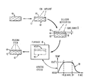
- a semiconductor device formed of a crystalline gallium arsenide wafer 10 is provided with a localised distribution of ion implanted impurities.
- the impurities provide desired electrical characteristics to the device.
- the GaAs wafer 10 has a substrate 12.
- the impurities typically are selected from dopant elements such as Si, Se, Be and Mg, and are placed in a layer 14 along the surface of the wafer 10 during a step of ion implantation which is accomplished in a well-known fashion by conventional implantation equipment.
- the impurities occupy sites within the lattice structure, their implantation introducing damage within the layer 14 of the semiconductor material. The damage is removed and the desired electrical characteristics are attained by a step of annealing at an elevated temperature in the range of approximately 700-1200°C.
- the step of annealing is preceded by a step of encapsulation of the layer 14 with a relatively thin layer 16 of silicon, the layer 16 being sufficiently thick to prevent the escape of arsenic from the semiconductor material under the annealing conditions.
- Silicon is advantageous because the coefficient of thermal expansion of the silicon is sufficiently close to that of GaAs, being approximately 2/3 that of GaAs, so as to bond well to the GaAs during the annealing process in spite of thermal expansions induced in each of the two layers 14 and 16 by the annealing conditions.
- a thickness of the silicon layer 16 in the range of 10-1,000 nm is adequate for containing the arsenic.
- a further advantage in the use of silicon as the encapsulant is the reduced chance for the development of cracks as compared with other capping materials such as Si0 2 and Si 3 N 4 .
- the silicon can be obtained in a pure form which permits accurate control of the composition of the cap provided by the layer 16 for more uniform results from run to run in the manufacturing process.
- the silicon cap can be applied to the GaAs by any one of the well known processes of sputtering, evaporation, and vapour deposition. Silicon can be readily removed from the GaAs by plasma etching with CF 4 or a mixture of CF 4 +O 2 .
- the desired selectivity in etching between silicon and GaAs is observed and/or expected for most fluorine based etchants, such as SF and C 2 F 6 .
- the CF does not etch the GaAs, thereby permitting complete removal of the encapsulating layer 16 after the annealing process to insure attainment of the expected electrical characteristics.
- the steps of implantation and capping are followed by the step of annealing, which step takes place in a furnace 18.
- the temperature is cycled from room or ambient to a value of approximately 850°c and back to room temperature.
- the annealing temperature of approximately 850°C is maintained for an annealing interval of approximately twenty minutes, as is shown in a graph 20 appended adjacent the furnace 18.
- the method of the invention applies generally to annealing situations wherein a nondiffusing Si cap is useful, and includes also rapid thermal annealing (annealing times of approximately 5-500 seconds), and laser annealing and electron beam annealing (annealing times approximately 1 nanosecond to 1 millisecond).
- the duration of the annealing interval is sufficient to remove damage in the lattice structure caused by the implantation of the dopant impurities. However, the annealing interval is sufficiently short to prevent all but an insignificant amount of diffusion of silicon from the cap layer 16 into the GaAs of the ion implantation layer 14.
- the manufacturing process continues with the final step of etching away the silicon cap layer 16 by a well known process of plasma etching using CF or CF 4 +0 2 as the etchant.
- the CF4 does not etch the GaAs in the ion implantation layer 16. Therefore, the etching process can be allowed to go to completion with complete removal of the silicon without danger of damaging the layer 16. This completes the process of fabricating the GaAs wafer 10 with the required layer 14 of impurities for providing the desired electrical characteristics.
- the aforementioned thickness of the silicon cap layer 16 is adequate to prevent escape of the As from the GaAs, it is noted that with thinner layers such as a layer having a thickness of approximately 10 nm, the presence of arsenic in the annealing environment is sufficient to induce some in-diffusion of silicon into the GaAs. The in-diffusion of silicon in the presence of arsenic results in a change in the implanted profile in the GaAs. However, the thinner layer of the silicon is sufficient to protect the GaAs surface from erosion during the annealing process.
- the capping of the invention is useful even with modifications of the foregoing manufacturing process.
- the Si layer can be applied before the ion implantation step in a situation such as that wherein the ion implantation is done directly through the capping layer to obtain a different doping profile.
- the capping can also be done with a small amount of oxygen or nitrogen or both because a layer with such impurity is still well matched to the GaAs.
- the use of the foregoing silicon capping layers on GaAs includes layers for protection or passivation as well as for ion implantation capping.
- the compatibility by Si and the well established technology of processing it makes it an excellent candidate for protecting GaAs wafers for storage purposes. That is to say, GaAs wafers after polishing are extremely sensitive to surface contamination and damage. Yet they often must be stored after this step for periods of time long enough to be affected by environmental conditions to which they are subjected. Coating with Si immediately after the final polishing step can serve as a protection against contamination and mechanical damage. The Si is easily removed by plasma etching before device processing, or may be left on as a passivating layer if desired.
Landscapes
- Junction Field-Effect Transistors (AREA)
- Weting (AREA)
Applications Claiming Priority (2)
| Application Number | Priority Date | Filing Date | Title |
|---|---|---|---|
| US705959 | 1985-02-27 | ||
| US06/705,959 US4615766A (en) | 1985-02-27 | 1985-02-27 | Silicon cap for annealing gallium arsenide |
Publications (1)
| Publication Number | Publication Date |
|---|---|
| EP0193021A1 true EP0193021A1 (fr) | 1986-09-03 |
Family
ID=24835634
Family Applications (1)
| Application Number | Title | Priority Date | Filing Date |
|---|---|---|---|
| EP86101712A Withdrawn EP0193021A1 (fr) | 1985-02-27 | 1986-02-11 | Procédé pour la formation d'un dispositif comportant de l'arsénide de gallium implanté |
Country Status (3)
| Country | Link |
|---|---|
| US (1) | US4615766A (fr) |
| EP (1) | EP0193021A1 (fr) |
| JP (1) | JPS61201425A (fr) |
Cited By (2)
| Publication number | Priority date | Publication date | Assignee | Title |
|---|---|---|---|---|
| GB2174108B (en) * | 1985-04-04 | 1989-07-19 | Sharp Kk | Method for forming a polycrystalline silicon thin film |
| FR2640079A1 (fr) * | 1988-12-01 | 1990-06-08 | Electronic & Telecomm Res Inst | Methode fabrication d'un transistor auto-aligne a semi-conducteur metallique (gaas) a effet de champ pourvu d'une grille en tungstene du type t |
Families Citing this family (27)
| Publication number | Priority date | Publication date | Assignee | Title |
|---|---|---|---|---|
| JPH0666454B2 (ja) * | 1985-04-23 | 1994-08-24 | インタ−ナショナル ビジネス マシ−ンズ コ−ポレ−ション | ▲iii▼―▲v▼族半導体デバイス |
| EP0216285B1 (fr) * | 1985-09-20 | 1992-05-13 | Sumitomo Electric Industries, Ltd. | Procédé de traitement thermique d'un substrat semi-conducteur composite |
| US4799392A (en) * | 1987-08-06 | 1989-01-24 | Motorola Inc. | Method for determining silicon (mass 28) beam purity prior to implantation of gallium arsenide |
| US4830983A (en) * | 1987-11-05 | 1989-05-16 | Xerox Corporation | Method of enhanced introduction of impurity species into a semiconductor structure from a deposited source and application thereof |
| US4824798A (en) * | 1987-11-05 | 1989-04-25 | Xerox Corporation | Method of introducing impurity species into a semiconductor structure from a deposited source |
| US4987095A (en) * | 1988-06-15 | 1991-01-22 | International Business Machines Corp. | Method of making unpinned oxide-compound semiconductor structures |
| US5086321A (en) * | 1988-06-15 | 1992-02-04 | International Business Machines Corporation | Unpinned oxide-compound semiconductor structures and method of forming same |
| US5188978A (en) * | 1990-03-02 | 1993-02-23 | International Business Machines Corporation | Controlled silicon doping of III-V compounds by thermal oxidation of silicon capping layer |
| DE69229265T2 (de) * | 1991-03-18 | 1999-09-23 | Trustees Of Boston University, Boston | Verfahren zur herstellung und dotierung hochisolierender dünner schichten aus monokristallinem galliumnitrid |
| US6953703B2 (en) * | 1991-03-18 | 2005-10-11 | The Trustees Of Boston University | Method of making a semiconductor device with exposure of sapphire substrate to activated nitrogen |
| US5633192A (en) * | 1991-03-18 | 1997-05-27 | Boston University | Method for epitaxially growing gallium nitride layers |
| US5294557A (en) * | 1991-08-26 | 1994-03-15 | The United States Of America As Represented By The Secretary Of The Navy | Implanting impurities in semiconductors and semiconductor implanted with impurities |
| US5306662A (en) * | 1991-11-08 | 1994-04-26 | Nichia Chemical Industries, Ltd. | Method of manufacturing P-type compound semiconductor |
| JP2540791B2 (ja) † | 1991-11-08 | 1996-10-09 | 日亜化学工業株式会社 | p型窒化ガリウム系化合物半導体の製造方法。 |
| US5336641A (en) * | 1992-03-17 | 1994-08-09 | Aktis Corporation | Rapid thermal annealing using thermally conductive overcoat |
| EP0952617B1 (fr) | 1993-04-28 | 2004-07-28 | Nichia Corporation | Dispositif semi-conducteur composé III-V comprenant des composés à base de nitrure de gallium |
| AU747260B2 (en) | 1997-07-25 | 2002-05-09 | Nichia Chemical Industries, Ltd. | Nitride semiconductor device |
| JP3770014B2 (ja) | 1999-02-09 | 2006-04-26 | 日亜化学工業株式会社 | 窒化物半導体素子 |
| ATE452445T1 (de) | 1999-03-04 | 2010-01-15 | Nichia Corp | Nitridhalbleiterlaserelement |
| US7642205B2 (en) | 2005-04-08 | 2010-01-05 | Mattson Technology, Inc. | Rapid thermal processing using energy transfer layers |
| TWI362769B (en) | 2008-05-09 | 2012-04-21 | Univ Nat Chiao Tung | Light emitting device and fabrication method therefor |
| US8273649B2 (en) | 2008-11-17 | 2012-09-25 | International Business Machines Corporation | Method to prevent surface decomposition of III-V compound semiconductors |
| US9576819B2 (en) * | 2014-06-17 | 2017-02-21 | Varian Semiconductor Equipment Associates, Inc. | Techniques for increased dopant activation in compound semiconductors |
| US9728934B2 (en) * | 2015-08-31 | 2017-08-08 | Avago Technologies General Ip (Singapore) Pte. Ltd. | Back-side-emitting vertical cavity surface emitting laser (VCSEL) wafer bonded to a heat-dissipation wafer, devices and methods |
| JP6394545B2 (ja) * | 2015-09-10 | 2018-09-26 | 豊田合成株式会社 | 半導体装置およびその製造方法ならびに電力変換装置 |
| US11670551B2 (en) * | 2019-09-26 | 2023-06-06 | Taiwan Semiconductor Manufacturing Co., Ltd. | Interface trap charge density reduction |
| US11501972B2 (en) * | 2020-07-22 | 2022-11-15 | Applied Materials, Inc. | Sacrificial capping layer for passivation using plasma-based implant process |
Citations (3)
| Publication number | Priority date | Publication date | Assignee | Title |
|---|---|---|---|---|
| DE2642413A1 (de) * | 1976-09-21 | 1978-03-23 | Siemens Ag | Verfahren zum aufbringen einer aus silicium bestehenden passivierungsschicht |
| US4267014A (en) * | 1980-02-29 | 1981-05-12 | The United States Of America As Represented By The Secretary Of The Navy | Semiconductor encapsulant for annealing ion-implanted GaAs |
| WO1986002488A1 (fr) * | 1984-10-09 | 1986-04-24 | American Telephone & Telegraph Company | REVETEMENT DE SEMICONDUCTEURS DE COMPOSES DE III-V et II-VI |
Family Cites Families (1)
| Publication number | Priority date | Publication date | Assignee | Title |
|---|---|---|---|---|
| JPS58103122A (ja) * | 1981-12-15 | 1983-06-20 | Nec Corp | 化合物半導体装置の製造方法 |
-
1985
- 1985-02-27 US US06/705,959 patent/US4615766A/en not_active Expired - Fee Related
- 1985-09-13 JP JP60201906A patent/JPS61201425A/ja active Pending
-
1986
- 1986-02-11 EP EP86101712A patent/EP0193021A1/fr not_active Withdrawn
Patent Citations (3)
| Publication number | Priority date | Publication date | Assignee | Title |
|---|---|---|---|---|
| DE2642413A1 (de) * | 1976-09-21 | 1978-03-23 | Siemens Ag | Verfahren zum aufbringen einer aus silicium bestehenden passivierungsschicht |
| US4267014A (en) * | 1980-02-29 | 1981-05-12 | The United States Of America As Represented By The Secretary Of The Navy | Semiconductor encapsulant for annealing ion-implanted GaAs |
| WO1986002488A1 (fr) * | 1984-10-09 | 1986-04-24 | American Telephone & Telegraph Company | REVETEMENT DE SEMICONDUCTEURS DE COMPOSES DE III-V et II-VI |
Non-Patent Citations (1)
| Title |
|---|
| PATENTS ABSTRACTS OF JAPAN, vol. 7, no. 204 (E-197) [1349], 9th September 1983, page 1349; & JP - A - 58 103 122 (NIPPON DENKI K.K.) 20-06-1983 * |
Cited By (2)
| Publication number | Priority date | Publication date | Assignee | Title |
|---|---|---|---|---|
| GB2174108B (en) * | 1985-04-04 | 1989-07-19 | Sharp Kk | Method for forming a polycrystalline silicon thin film |
| FR2640079A1 (fr) * | 1988-12-01 | 1990-06-08 | Electronic & Telecomm Res Inst | Methode fabrication d'un transistor auto-aligne a semi-conducteur metallique (gaas) a effet de champ pourvu d'une grille en tungstene du type t |
Also Published As
| Publication number | Publication date |
|---|---|
| US4615766A (en) | 1986-10-07 |
| JPS61201425A (ja) | 1986-09-06 |
Similar Documents
| Publication | Publication Date | Title |
|---|---|---|
| US4615766A (en) | Silicon cap for annealing gallium arsenide | |
| US5244819A (en) | Method to getter contamination in semiconductor devices | |
| US5234850A (en) | Method of fabricating a nitride capped MOSFET for integrated circuits | |
| US5194397A (en) | Method for controlling interfacial oxide at a polycrystalline/monocrystalline silicon interface | |
| US4634474A (en) | Coating of III-V and II-VI compound semiconductors | |
| US4105805A (en) | Formation of metal nitride oxide semiconductor (MNOS) by ion implantation of oxygen through a silicon nitride layer | |
| US4332627A (en) | Method of eliminating lattice defects in a semiconductor device | |
| US5279973A (en) | Rapid thermal annealing for semiconductor substrate by using incoherent light | |
| US4662956A (en) | Method for prevention of autodoping of epitaxial layers | |
| US4902642A (en) | Epitaxial process for silicon on insulator structure | |
| KR100396609B1 (ko) | 반도체기판의처리방법 | |
| US4199386A (en) | Method of diffusing aluminum into monocrystalline silicon | |
| US3945856A (en) | Method of ion implantation through an electrically insulative material | |
| US4819039A (en) | Devices and device fabrication with borosilicate glass | |
| US4267014A (en) | Semiconductor encapsulant for annealing ion-implanted GaAs | |
| US4137141A (en) | Process for producing a silicon nitride diffusion barrier on a semiconductor substrate, particularly III-V semiconductor substrates | |
| US4050967A (en) | Method of selective aluminum diffusion | |
| US6498079B1 (en) | Method for selective source diffusion | |
| US4784964A (en) | EPI defect reduction using rapid thermal annealing | |
| JPS6227727B2 (fr) | ||
| EP0219243A2 (fr) | Procédé pour la fabrication d'un transistor bipolaire | |
| JPH039612B2 (fr) | ||
| US5849630A (en) | Process for forming ohmic contact for III-V semiconductor devices | |
| GB2307790A (en) | Method of removing defects from semiconductor devices. | |
| JPS60227416A (ja) | 半導体基板のアニ−ル方法 |
Legal Events
| Date | Code | Title | Description |
|---|---|---|---|
| PUAI | Public reference made under article 153(3) epc to a published international application that has entered the european phase |
Free format text: ORIGINAL CODE: 0009012 |
|
| AK | Designated contracting states |
Kind code of ref document: A1 Designated state(s): DE FR GB |
|
| 17P | Request for examination filed |
Effective date: 19861212 |
|
| 17Q | First examination report despatched |
Effective date: 19881104 |
|
| STAA | Information on the status of an ep patent application or granted ep patent |
Free format text: STATUS: THE APPLICATION HAS BEEN WITHDRAWN |
|
| 18W | Application withdrawn |
Withdrawal date: 19890608 |
|
| R18W | Application withdrawn (corrected) |
Effective date: 19890608 |
|
| RIN1 | Information on inventor provided before grant (corrected) |
Inventor name: JACKSON, THOMAS NELSON Inventor name: PEPPER, GWEN Inventor name: RUTZ, RICHARD FREDERICK |