EP0193156A2 - Câble flexible et méthode de fabrication de celui-ci - Google Patents
Câble flexible et méthode de fabrication de celui-ci Download PDFInfo
- Publication number
- EP0193156A2 EP0193156A2 EP86102366A EP86102366A EP0193156A2 EP 0193156 A2 EP0193156 A2 EP 0193156A2 EP 86102366 A EP86102366 A EP 86102366A EP 86102366 A EP86102366 A EP 86102366A EP 0193156 A2 EP0193156 A2 EP 0193156A2
- Authority
- EP
- European Patent Office
- Prior art keywords
- flexible cable
- copper foil
- pattern
- base
- foil pattern
- Prior art date
- Legal status (The legal status is an assumption and is not a legal conclusion. Google has not performed a legal analysis and makes no representation as to the accuracy of the status listed.)
- Granted
Links
Images


Classifications
-
- H—ELECTRICITY
- H01—ELECTRIC ELEMENTS
- H01B—CABLES; CONDUCTORS; INSULATORS; SELECTION OF MATERIALS FOR THEIR CONDUCTIVE, INSULATING OR DIELECTRIC PROPERTIES
- H01B7/00—Insulated conductors or cables characterised by their form
- H01B7/08—Flat or ribbon cables
- H01B7/0838—Parallel wires, sandwiched between two insulating layers
-
- H—ELECTRICITY
- H05—ELECTRIC TECHNIQUES NOT OTHERWISE PROVIDED FOR
- H05K—PRINTED CIRCUITS; CASINGS OR CONSTRUCTIONAL DETAILS OF ELECTRIC APPARATUS; MANUFACTURE OF ASSEMBLAGES OF ELECTRICAL COMPONENTS
- H05K1/00—Printed circuits
- H05K1/02—Details
- H05K1/0213—Electrical arrangements not otherwise provided for
- H05K1/0215—Grounding of printed circuits by connection to external grounding means
-
- H—ELECTRICITY
- H05—ELECTRIC TECHNIQUES NOT OTHERWISE PROVIDED FOR
- H05K—PRINTED CIRCUITS; CASINGS OR CONSTRUCTIONAL DETAILS OF ELECTRIC APPARATUS; MANUFACTURE OF ASSEMBLAGES OF ELECTRICAL COMPONENTS
- H05K1/00—Printed circuits
- H05K1/02—Details
- H05K1/0213—Electrical arrangements not otherwise provided for
- H05K1/0254—High voltage adaptations; Electrical insulation details; Overvoltage or electrostatic discharge protection ; Arrangements for regulating voltages or for using plural voltages
- H05K1/0257—Overvoltage protection
- H05K1/0259—Electrostatic discharge [ESD] protection
-
- H—ELECTRICITY
- H05—ELECTRIC TECHNIQUES NOT OTHERWISE PROVIDED FOR
- H05K—PRINTED CIRCUITS; CASINGS OR CONSTRUCTIONAL DETAILS OF ELECTRIC APPARATUS; MANUFACTURE OF ASSEMBLAGES OF ELECTRICAL COMPONENTS
- H05K1/00—Printed circuits
- H05K1/02—Details
- H05K1/11—Printed elements for providing electric connections to or between printed circuits
- H05K1/117—Pads along the edge of rigid circuit boards, e.g. for pluggable connectors
-
- H—ELECTRICITY
- H05—ELECTRIC TECHNIQUES NOT OTHERWISE PROVIDED FOR
- H05K—PRINTED CIRCUITS; CASINGS OR CONSTRUCTIONAL DETAILS OF ELECTRIC APPARATUS; MANUFACTURE OF ASSEMBLAGES OF ELECTRICAL COMPONENTS
- H05K1/00—Printed circuits
- H05K1/02—Details
- H05K1/11—Printed elements for providing electric connections to or between printed circuits
- H05K1/118—Printed elements for providing electric connections to or between printed circuits specially for flexible printed circuits, e.g. using folded portions
-
- H—ELECTRICITY
- H05—ELECTRIC TECHNIQUES NOT OTHERWISE PROVIDED FOR
- H05K—PRINTED CIRCUITS; CASINGS OR CONSTRUCTIONAL DETAILS OF ELECTRIC APPARATUS; MANUFACTURE OF ASSEMBLAGES OF ELECTRICAL COMPONENTS
- H05K2201/00—Indexing scheme relating to printed circuits covered by H05K1/00
- H05K2201/09—Shape and layout
- H05K2201/09209—Shape and layout details of conductors
- H05K2201/0929—Conductive planes
- H05K2201/09354—Ground conductor along edge of main surface
-
- H—ELECTRICITY
- H05—ELECTRIC TECHNIQUES NOT OTHERWISE PROVIDED FOR
- H05K—PRINTED CIRCUITS; CASINGS OR CONSTRUCTIONAL DETAILS OF ELECTRIC APPARATUS; MANUFACTURE OF ASSEMBLAGES OF ELECTRICAL COMPONENTS
- H05K3/00—Apparatus or processes for manufacturing printed circuits
- H05K3/22—Secondary treatment of printed circuits
- H05K3/28—Applying non-metallic protective coatings
Definitions
- the present invention relates to a flexible cable having excellent dielectric strength static electricity and a method of manufacturing thereof.
- flexible printed circuit boards have come to be profitably employed in various fields as important parts for use in mounting thereon many electronic circuitries being central to computer application thereof such as circuit boards and wiring parts, etc.
- Such a flexible printed circuit board when employed as a circuit board is multilayer- structured and adapted to mount electronic parts directly thereon, while it is miniaturized and made lightweight by making use of its flexible structure as well as put in order within a limited space for higher density mounting.
- the flexible printed board is adapted to wire together individual connections in wire harness as being useful for elimination or reduction of labor as well as prevention of erroneous wiring.
- it is also widely used for wiring various movable portions in view of flexible and lightweight structure thereof.
- a flexible cable has a conducting part 1 thereof, a terminal 2 being an extension of the conducting part 1, and a lug 3 for attaching thereto a setscrew having a locking hole 4.
- the flexible cable is mounted on a base 5 comprising a high polymer material such as polyester and polyimide.
- the base 5 is of a - flame-retardant with thickness of several tens of a micrometer.
- Designated at 6 is a copper foil pattern formed as the conducting part 1 and patterned by subjecting the copper foil bonded onto the base 5 to etching.
- a cover laying 7 formed by the same material as that of the base 5 is arranged to cover the copper foil pattern 6 on the base 5 therewith.
- Designated at 8 is an insulator part comprising the base 5 and the cover laying 7. Since the terminal part 2 is brought into contact with a pattern of any other counter part, the base material (not shown) and the cover laying 7 are eliminated at this place. Moreover, the terminal 2 , since deteriorated in its contact resistance, is further subjected to processing such as gold plating.
- the copper foil pattern 6 is constructed to keep an interval capable of securing dielectric strength against the adjoining portion of the copper foil pattern while keeping a distance (distance between edges) away from both sides of the insulator 8.
- the cover laying 7 and the copper foil pattern 6 respectively have their thicknesses of about several tens of a micrometer and are sufficiently bending-resistant. Accordingly, the flexible cable is in wide use as a code for transmitting an electric signal to a mechanically movable portion including a printer carriage cable.
- Another object of the present invention is to provide a flexible cable capable of preventing an electronic circuit connected with the conductive part from being broken, even if the cover laying is subjected to dielectric breakdown owing to its exposure to static electricity of high voltage to cause electric discharge in the conductive part to be produced.
- Still another object of the present invention is to provide a method of manufacturing a flexible cable capable of preventing electric discharge from being produced in the conductive part due to dielectric breakdown of the cover laying caused by static electricity of high voltage.
- a flexible cable provided with a pattern to be used as FG is exposed at least partly -to a signal line therealong and extended to terminals.
- the pattern is directly connected to FG etc. to be grounded via connectors. etc..
- a flexible cable comprising a base, a conductor and a cover laying composed of a plurality of pattern and being laminate and bonded, wherein the cover laying is bonded so as to at least one position of the pattern is exposed in the extending direction of the pattern.
- a flexible cable comprising a base, a conductor and a cover laying composed of a plurality of pattern and being laminated and bonded, wherein an outer shape of the flexible cable is cut off along both sides or one side of the flexible cable so that the pattern is exposed.
- spark discharge is caused, before any spark discharge is produced between the subject and each 3f the different portions of the conducting pattern for use in signal lines, among the subject and portions of the pattern serving as a ground line, as at least partly exposing the flexible cable to the outside. Accordingly, dielectric breakdown of the insulator part caused by static electricity of high voltage, i.e., dielectric breakdown of an electric circuit of any apparatus connected with portions of the pattern usable for a signal line can be prevented.
- a flexible cable having a conducting part comprising a plurality of different portions of the pattern can be manufactured with ease while permitting cover laying to be laminated on a prescribed portion of the pattern so as to permit the above pattern portion to be at least partly exposed to the outside in its extending direction.
- a flexible cable having a conductive part comprising a plurality of different portions of the pattern can be manufactured with ease since the outer shape of the flexible cable is to be cut out together with the pattern whereby pattern edges located along both sides of the flexible cable or those along any one of the sides are exposed.
- the flexible cable shown here has a copper foil pattern newly formed fully extending to both sides of the flexible cable of Fig. 1.
- copper foil pattern 11 exposed in its edges to the outside is newly formed on the conductive part 1 while fully extending to both sides of the flexible cable previously formed, in addition to copper foil patterns 6 used as usual signal lines, and,furthermore, is extended to the terminals 2 or to the lug holes 10.
- the cover laying 7 is eliminated at locking holes 10 and at the terminals 2.
- the copper foil patterns 11 exposed to edges of both sides of the flexible cable are adapted to run to peripheral edges of the locking holes 10 and covered with the cover laying 7 in their upper parts.
- an electric discharge route is shown as static electricity having high voltage (e.g., 10 to 20 k V ) is brought near the flexible cable.
- a base comprising a high polymer material such as polyester, etc., and copper foils are first prepared, and in Step 101 the copper foils 116 are bonded to the base and laminated on the base 105.
- the laminated copper foils are subjected to etching to form copper foil patterns 6 and 11 on the base 105.
- the cover laying 7 is bonded to the base 105 on the side of copper foil patterns6, 11 of the base 105 to cover the copper foil patterns 6 and 11 therewith.
- the flexible cable so formed is cut off into a prescribed shape. In the instance, the copper foil pattern 11, i.e., a pattern for grounding is cut off so as to be exposed on both sides of the flexible case.
- Step 104 is particularly important for the method of manufacturing the flexible cable according to the present invention wherein the copper pattern 11 is cut off while partly left behind and at least one copper foil pattern 11 may be cut off.
- the cover laying 71 is bonded to the base 5 so as to cover only the copper foil pattern 6 while leaving the copper foil pattern 11 exposed.
- This processing is effected in the Step 103 in this case.
- the copper foil pattern 11 is not necessarily needed to be cut off in Step 104.
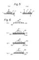
- the copper foil pattern used for a grounding conductor is provided, in Fig. 5(a), on both sides or one side of the flexible, while in Fig. 5(b) it is provided inside the flexible cable.
- a base comprising a high polymer material such as polyester, etc., and a cover laying are first prepared, and in Step 201 a plurality of thin metal sheet conductors 211, 212 being conducting parts of the cable are aligned in spaced relation in a prescribed interval by making use of a jig.
- Step 202 the metal sheet conductors 211, 212 are put between a base 214 and a cover laying 213 in a sandwiching relation and laminated.
- Step 203 the base 214 and the cover laying 213 are subjected to thermocompression bonding from both sides thereof to fix the metal sheet conductors 211, 212.
- Step 204 the flexible cable so constructed is cut off into a prescribed shape. In the instance, the flexible cable is cut off such that the metal sheet conductor 212, i.e., the pattern for grounding is exposed on both side ends of the flexible cable. Thereupon, any one of the metal sheet conductors 212 on both sides of the flexible cable may be cut off.
- the cover laying 213 may cover only the metal sheet conductor 211 while the metal sheet conductor 212 may be exposed. Thereupon, it is only normal that in Step 204 the metal sheet conductor 212 may not be cut off. This case corresponds to that of Fig. 5(a).
- the metal sheet conductor 212 may be disposed inside the flexible cable. This case corresponds to that of Fig. 5(b).
Landscapes
- Engineering & Computer Science (AREA)
- Microelectronics & Electronic Packaging (AREA)
- Insulated Conductors (AREA)
Applications Claiming Priority (2)
| Application Number | Priority Date | Filing Date | Title |
|---|---|---|---|
| JP34503/85 | 1985-02-25 | ||
| JP60034503A JPS61195507A (ja) | 1985-02-25 | 1985-02-25 | フレキシブルケ−ブルおよびその製造方法 |
Publications (3)
| Publication Number | Publication Date |
|---|---|
| EP0193156A2 true EP0193156A2 (fr) | 1986-09-03 |
| EP0193156A3 EP0193156A3 (en) | 1989-03-01 |
| EP0193156B1 EP0193156B1 (fr) | 1992-05-06 |
Family
ID=12416055
Family Applications (1)
| Application Number | Title | Priority Date | Filing Date |
|---|---|---|---|
| EP86102366A Expired EP0193156B1 (fr) | 1985-02-25 | 1986-02-24 | Câble flexible et méthode de fabrication de celui-ci |
Country Status (4)
| Country | Link |
|---|---|
| US (1) | US4748293A (fr) |
| EP (1) | EP0193156B1 (fr) |
| JP (1) | JPS61195507A (fr) |
| DE (1) | DE3685135D1 (fr) |
Families Citing this family (25)
| Publication number | Priority date | Publication date | Assignee | Title |
|---|---|---|---|---|
| JPS62124571U (fr) * | 1986-01-31 | 1987-08-07 | ||
| DE3932860A1 (de) * | 1989-10-02 | 1991-04-11 | Thomson Brandt Gmbh | Spulenanordnung |
| JPH0491924U (fr) * | 1990-12-26 | 1992-08-11 | ||
| US5238006A (en) * | 1991-06-24 | 1993-08-24 | Medtronic, Inc. | Apnea stimulation lead |
| JPH0781182A (ja) * | 1993-09-20 | 1995-03-28 | Seiko Epson Corp | シリアルプリンタのキャリッジ駆動装置 |
| US5811727A (en) * | 1995-10-16 | 1998-09-22 | Lo; Jeffrey | In-line coupler |
| US5847324A (en) * | 1996-04-01 | 1998-12-08 | International Business Machines Corporation | High performance electrical cable |
| US6841735B1 (en) * | 1996-04-03 | 2005-01-11 | Methode Electronics, Inc. | Flat cable and modular rotary anvil to make same |
| US6026563A (en) | 1996-04-03 | 2000-02-22 | Methode Electronics, Inc. | Method of making flat cable |
| US6643918B2 (en) * | 2000-04-17 | 2003-11-11 | Shielding For Electronics, Inc. | Methods for shielding of cables and connectors |
| KR100733877B1 (ko) * | 2000-07-06 | 2007-07-02 | 엘지.필립스 엘시디 주식회사 | 가요성 인쇄회로 필름 |
| EP1454153A2 (fr) * | 2001-12-14 | 2004-09-08 | Intest IP Corporation | Interface interne a tete temoin flexible |
| US6867668B1 (en) * | 2002-03-18 | 2005-03-15 | Applied Micro Circuits Corporation | High frequency signal transmission from the surface of a circuit substrate to a flexible interconnect cable |
| JP3936925B2 (ja) * | 2003-06-30 | 2007-06-27 | 日本オプネクスト株式会社 | 光伝送モジュール |
| DE10331710B4 (de) * | 2003-07-11 | 2008-05-08 | W. L. Gore & Associates Gmbh | Bandkabel |
| US7223922B2 (en) * | 2004-07-28 | 2007-05-29 | International Business Machines Corporation | ESD dissipative coating on cables |
| US8405950B2 (en) * | 2008-05-21 | 2013-03-26 | International Business Machines Corporation | Cable having ESD dissipative layer electrically coupled to leads thereof |
| DE202009005428U1 (de) * | 2009-04-14 | 2009-06-04 | Dula-Werke Dustmann & Co. Gmbh | Vorrichtung zur Zufuhr elektrischer Energie an einen Verbraucher |
| JP5206630B2 (ja) * | 2009-08-27 | 2013-06-12 | 日立電線株式会社 | フレキシブルハーネスを用いた電気的接続部品及び電気的接続方法 |
| US8844537B1 (en) | 2010-10-13 | 2014-09-30 | Michael T. Abramson | System and method for alleviating sleep apnea |
| JP6146998B2 (ja) * | 2012-12-21 | 2017-06-14 | キヤノン株式会社 | 電子機器 |
| ITUD20130085A1 (it) * | 2013-06-20 | 2014-12-21 | Eliwell Controls S R L Con Unico S Ocio | Strumento elettronico di misura, condizionamento e regolazione, e relativo procedimento di realizzazione |
| US10057980B2 (en) * | 2016-03-15 | 2018-08-21 | Cisco Technology, Inc. | Method and apparatus for reducing corrosion in flat flexible cables and flexible printed circuits |
| CN207321622U (zh) * | 2017-06-06 | 2018-05-04 | 惠科股份有限公司 | 一种应用于显示面板的软性电路板和显示装置 |
| US20240274323A1 (en) * | 2021-09-29 | 2024-08-15 | Saint-Gobain Glass France | Ribbon cable for detecting a break, connection assembly with composite panel, method for detecting a break, and use of the ribbon cable |
Family Cites Families (12)
| Publication number | Priority date | Publication date | Assignee | Title |
|---|---|---|---|---|
| US3107197A (en) * | 1956-04-18 | 1963-10-15 | Int Resistance Co | Method of bonding a metal to a plastic and the article produced thereby |
| US3168617A (en) * | 1962-08-27 | 1965-02-02 | Tape Cable Electronics Inc | Electric cables and method of making the same |
| US3391246A (en) * | 1964-03-16 | 1968-07-02 | Westinghouse Electric Corp | Multiconductor flat cables |
| US3523844A (en) * | 1967-01-20 | 1970-08-11 | Thomas & Betts Corp | Method and apparatus for making flexible multiconductor flat cable |
| US3576723A (en) * | 1968-04-23 | 1971-04-27 | Nasa | Method of making shielded flat cable |
| US3704164A (en) * | 1968-06-19 | 1972-11-28 | Electro Connective Systems Inc | Printed circuitry |
| GB1266402A (fr) * | 1969-03-18 | 1972-03-08 | ||
| GB1390923A (en) * | 1971-08-17 | 1975-04-16 | Elliott Brothers London Ltd | Manufacture of cableforms |
| US3891955A (en) * | 1974-05-07 | 1975-06-24 | Westinghouse Electric Corp | Electrical inductive apparatus |
| US4209215A (en) * | 1978-11-24 | 1980-06-24 | Hughes Aircraft Company | Mass terminable shielded flat flexible cable and method of making such cables |
| JPS55117877U (fr) * | 1979-02-09 | 1980-08-20 | ||
| US4564723A (en) * | 1983-11-21 | 1986-01-14 | Allied Corporation | Shielded ribbon cable and method |
-
1985
- 1985-02-25 JP JP60034503A patent/JPS61195507A/ja active Granted
-
1986
- 1986-02-24 DE DE8686102366T patent/DE3685135D1/de not_active Expired - Lifetime
- 1986-02-24 EP EP86102366A patent/EP0193156B1/fr not_active Expired
- 1986-02-25 US US06/832,753 patent/US4748293A/en not_active Expired - Lifetime
Also Published As
| Publication number | Publication date |
|---|---|
| JPH0429163B2 (fr) | 1992-05-18 |
| US4748293A (en) | 1988-05-31 |
| DE3685135D1 (de) | 1992-06-11 |
| EP0193156A3 (en) | 1989-03-01 |
| EP0193156B1 (fr) | 1992-05-06 |
| JPS61195507A (ja) | 1986-08-29 |
Similar Documents
| Publication | Publication Date | Title |
|---|---|---|
| EP0193156A2 (fr) | Câble flexible et méthode de fabrication de celui-ci | |
| US6777622B2 (en) | Wiring boards | |
| US4054939A (en) | Multi-layer backpanel including metal plate ground and voltage planes | |
| US5414220A (en) | Flexible wiring cable | |
| US7569773B2 (en) | Wired circuit board | |
| KR100487052B1 (ko) | 배선 기판 및 배선 기판 제조 방법 | |
| US5748209A (en) | Thermal ink jet tab circuit having a plurality of trace groups wherein adjacent traces in each group are staggered | |
| EP0269232B1 (fr) | Connecteur pour câble de transmission ayant une enveloppe profilée | |
| US5306874A (en) | Electrical interconnect and method of its manufacture | |
| US6185105B1 (en) | Discharge structure of printed circuit board | |
| EP0737025A1 (fr) | Carte a circuits imprimes | |
| US5250757A (en) | Printed wiring board having a connecting terminal | |
| JP2002203431A (ja) | フラットハーネス | |
| JPH0750499A (ja) | フレキシブル印刷配線板のシールド装置 | |
| WO1999012223A1 (fr) | Procede et agencement dans un systeme electronique | |
| JP3374630B2 (ja) | フラットケーブル | |
| EP0441376A2 (fr) | GénÀ©rateur de fréquence | |
| JPH08190812A (ja) | フラットシールド回路体及びその製造方法 | |
| KR900009645Y1 (ko) | 프린트 배선기판 | |
| EP0430842A2 (fr) | Appareil et procédé pour retravailler des plaquettes de circuits imprimés | |
| JPH021778Y2 (fr) | ||
| JPH0710970U (ja) | フレキシブルプリント配線基板の接続構造 | |
| JPS6284586A (ja) | フレキシブル配線基板の製造方法 | |
| JPH07294586A (ja) | プリント配線板の導通検査用ピッチ変換板の製造方法及びその変換板を用いた導通検査方法 | |
| JPH08285889A (ja) | 半導体装置検査用治具及びその製造方法 |
Legal Events
| Date | Code | Title | Description |
|---|---|---|---|
| PUAI | Public reference made under article 153(3) epc to a published international application that has entered the european phase |
Free format text: ORIGINAL CODE: 0009012 |
|
| AK | Designated contracting states |
Kind code of ref document: A2 Designated state(s): DE FR GB |
|
| PUAL | Search report despatched |
Free format text: ORIGINAL CODE: 0009013 |
|
| AK | Designated contracting states |
Kind code of ref document: A3 Designated state(s): DE FR GB |
|
| 17P | Request for examination filed |
Effective date: 19890721 |
|
| 17Q | First examination report despatched |
Effective date: 19900824 |
|
| GRAA | (expected) grant |
Free format text: ORIGINAL CODE: 0009210 |
|
| AK | Designated contracting states |
Kind code of ref document: B1 Designated state(s): DE FR GB |
|
| REF | Corresponds to: |
Ref document number: 3685135 Country of ref document: DE Date of ref document: 19920611 |
|
| ET | Fr: translation filed | ||
| PLBE | No opposition filed within time limit |
Free format text: ORIGINAL CODE: 0009261 |
|
| STAA | Information on the status of an ep patent application or granted ep patent |
Free format text: STATUS: NO OPPOSITION FILED WITHIN TIME LIMIT |
|
| 26N | No opposition filed | ||
| REG | Reference to a national code |
Ref country code: GB Ref legal event code: IF02 |
|
| PGFP | Annual fee paid to national office [announced via postgrant information from national office to epo] |
Ref country code: FR Payment date: 20050208 Year of fee payment: 20 |
|
| PGFP | Annual fee paid to national office [announced via postgrant information from national office to epo] |
Ref country code: DE Payment date: 20050217 Year of fee payment: 20 |
|
| PGFP | Annual fee paid to national office [announced via postgrant information from national office to epo] |
Ref country code: GB Payment date: 20050223 Year of fee payment: 20 |
|
| REG | Reference to a national code |
Ref country code: GB Ref legal event code: PE20 |
|
| PG25 | Lapsed in a contracting state [announced via postgrant information from national office to epo] |
Ref country code: GB Free format text: LAPSE BECAUSE OF EXPIRATION OF PROTECTION Effective date: 20060223 |