EP0194185A2 - Système d'ordinateur avec configuration de surveillance d'instruction - Google Patents
Système d'ordinateur avec configuration de surveillance d'instruction Download PDFInfo
- Publication number
- EP0194185A2 EP0194185A2 EP86400332A EP86400332A EP0194185A2 EP 0194185 A2 EP0194185 A2 EP 0194185A2 EP 86400332 A EP86400332 A EP 86400332A EP 86400332 A EP86400332 A EP 86400332A EP 0194185 A2 EP0194185 A2 EP 0194185A2
- Authority
- EP
- European Patent Office
- Prior art keywords
- instruction
- control
- subinstruction
- address
- codes
- Prior art date
- Legal status (The legal status is an assumption and is not a legal conclusion. Google has not performed a legal analysis and makes no representation as to the accuracy of the status listed.)
- Ceased
Links
Images


Classifications
-
- G—PHYSICS
- G06—COMPUTING OR CALCULATING; COUNTING
- G06F—ELECTRIC DIGITAL DATA PROCESSING
- G06F11/00—Error detection; Error correction; Monitoring
- G06F11/30—Monitoring
-
- G—PHYSICS
- G06—COMPUTING OR CALCULATING; COUNTING
- G06F—ELECTRIC DIGITAL DATA PROCESSING
- G06F9/00—Arrangements for program control, e.g. control units
- G06F9/06—Arrangements for program control, e.g. control units using stored programs, i.e. using an internal store of processing equipment to receive or retain programs
- G06F9/22—Microcontrol or microprogram arrangements
- G06F9/26—Address formation of the next micro-instruction ; Microprogram storage or retrieval arrangements
- G06F9/262—Arrangements for next microinstruction selection
- G06F9/268—Microinstruction selection not based on processing results, e.g. interrupt, patch, first cycle store, diagnostic programs
Definitions
- the present invention relates to a computer system, more particularly, to a computer system having a microprogram instruction surveillance configuration.
- a plurality of microprogram instructions are provided in addition to the corresponding macro instructions, such as a LOAD instruction or a STORE instruction.
- One of the microprogram instructions can be used as a single macro instruction in programs, simplifying use thereof.
- Each microprogram instruction consists of a plurality of subinstructions (or microinstructions), and thus can provide a composite function which cannot be performed by a macro instruction.
- the operation thereof differs from that of a normal macro instruction. Accordingly, a special logic circuit effecting the microprogram instructions must be provided in the computer system.
- Japanese Unexamined Patent Publication No. 58-195252 discloses a microprogram control apparatus for stopping the operation of a subinstruction during the execution of a microprogram instruction when an address of the subinstruction coincides with a set.-address to be - stopped.
- the control apparatus stops the generation of a clock pulse. Accordingly, there may be trouble in the restart operation-
- the control apparatus also lacks surveillance functions for analyzing trouble quickly and efficiently.
- An object of the present invention is to provide a computer system having an instruction surveillance configuration performing control of microprogram instructions and subinstructions forming the microprogram instructions.
- Another object of the present invention is to provide a computer system having an instruction surveillance configuration performing the trace of operations of the microprogram instructions and subinstructions.
- Still another object of the present invention is to provide a computer system having an instruction surveillance configuration including the above functions with a simple and small circuit configuration and ease of use.
- a computer system including a unit processing instructions containing microprogram instructions, including a first circuit storing at least one instruction code group having a plurality of subinstruction codes performing a corresponding microprogram instruction; a second circuit operatively connected to the instruction code store circuit, decoding a microprogram instruction, and advancing an address of subinstructions of the microprogram instruction, defined by the subinstruction codes, in response to contents of the subinstruction codes; and a third circuit operatively connected to the instruction code store circuit and the instruction decode circuit, executing the subinstructions in response to subinstruction codes from the instruction code store circuit.
- the instruction code store circuit further stores a plurality of other subinstruction codes performing control of the instruction processing circuit.
- the computer system also includes a control unit operatively connected to the instruction processing circuit, comparing an address preset thereto and another address from the instruction decode circuit designating the subinstruction codes in the instruction code store circuit, and stopping the operation of the subinstruction and supplying at least one control data including control bits and an address designating the other subinstruction codes in the instruction code store circuit when the preset address coincides with the other address.
- the third circuit executes subinstruction of the other subinstruction codes in response to the control bits in the control data.
- the control unit may restore the stopped operation of the subinstruction when a reset signal is supplied thereto.
- the computer system may include a bus interface unit, operatively connected to the instruction processing unit and the control unit through a data bus.
- the control unit may also include a memory storing the control data.
- the bus interface unit stores a plurality of control data to the memory and sets the preset address to the control unit through the data bus in response to an application of control signals, so that the third circuit continuously executes the other subinstructions corresponding to addresses of the control data in response to control bits of the control data when the preset address coincides with the other address from the instruction decode circuit.
- the control circuit may include a register holding the preset address, a compare circuit comparing the preset address and another address from the instruction decode circuit and outputting a coincidence signal when the preset address coincides with another address, a latch circuit latching the coincidence signal, a first gate gating another address passing therethrough, a second gate gating the control data passing therethrough, and a switch circuit.
- the first gate and said second gate are operated reversely in response to the coincidence signal, the first gate becoming a closed state passing another address therethrough when the coincidence signal is disable. Otherwise, the second gate passes the control data from the memory therethrough.
- the switch circuit supplies the other address to the compare circuit when the coincidence signal is disable. Otherwise, the control data is supplied to the instruction code store circuit through the instruction decode circuit.
- a computer system including a unit processing instructions containing microprogram instructions, including a circuit storing at least one instruction code group having a plurality of subinstruction codes performing a corresponding microprogram instruction; a circuit, operatively connected to the instruction code store circuit, decoding a microprogram instruction, and advancing an address of subinstructions of the microprogram instruction, defined by the subinstruction codes, in response to contents of the subinstruction codes; and a circuit, operatively connected to the instruction code store circuit and the instruction decode circuit, executing the subinstructions in response to subinstruction codes from the instruction code store circuit.
- the computer system also includes a control unit, operatively connected to the instruction processing circuit, storing the subinstruction codes from instruction decode circuit, and outputting the same in response to control signals.
- the control unit may store data combined with an address of the subinstruction code and control states in the instruction processing circuit and output the same.
- a computer system including a control unit, operatively connected to the instruction processing circuit, comparing an address preset thereto and another address from the instruction decode unit designating the subinstruction codes in the instruction code store circuit, stopping the operation of the subinstruction when the preset address coincides with the other address.
- the control unit may restore the stopped operation of said subinstruction when a reset signal is supplied thereto.
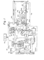
- a computer system includes a microprocessor unit (MPU) 10, a bus interface unit (BIU) 20, a main memory chip (CHIP) 30, an external signal input circuit (EXT) 35,.a microprogram instruction surveillance unit (MIS) 40, a data bus (DATA-BUS) 100, and an address bus (ADD-BUS) 101.
- MPU microprocessor unit
- BIU bus interface unit
- CHIP main memory chip
- EXT external signal input circuit
- MIS microprogram instruction surveillance unit
- DATA-BUS data bus
- ADD-BUS address bus
- the MPU 10 includes an instruction register (IR) 1 of 16 bits, a microaddress register (MAR) 2 of 16 bits, a decoder (DEC) 3, a microprogram code storage (MCS) 4, a sequencer (SEQ) 5, and an instruction execution unit (EU) 6.
- the MCS 4 stores a plurality of subinstruction groups each consisting of a plurality of subinstructions corresponding to a microprogram instruction.
- the MCS 4 consists of two regions 4a and 4b, the former 4a being accessible by the programs, however, the latter 4b not being accessible.
- the EU 6 includes an arithmetic operation logic circuit unit (ALU) 61, a temporary register b (T-REG.b) 62 of 16 bits, a temporary register a (T-REG.a) 63 of 16 bits and consisting of a higher 8-bit register (aH) and a lower 8-bit register (aL), and four general registers (G-REG.A to G-REG.D) 65 to 68.
- G-REG.A to G-REG.D can be accessed by the programs through instructions containing normal single instructions and the microprogram instructions, however, the IR, the MAR, and the T-REG a and b cannot.
- the BIU 20 includes a communication register 2 (COM- R2) 21 of 16 bits and Q-registers (QI-REG to Q3-REG) 22 to 24, each of 16 bits.
- COM-R2 and QI-REG to Q3-REG cannot accessed by the programs.
- the MIS 40 includes a break point register (BPR) 41 having an enable (EN) bit, a bus switching circuit (SW) 42 switching internal buses 112 and 113, an exclusive NOR circuit (ENOR) 43, a set-reset type flip-flop circuit (FF) 44 including a NOR gate and a NAND gate connected between them forming the set-reset flip-flop, a NAND gate (NAND) 45, and an inverter (INV) 46.
- the MIS 40 also includes output gates -47 and 48 and an FIFO memory 49.
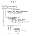
- Figure 2 is a view illustrating a configuration of data stored in the FIFO memory 49.
- the FIFO memory 49 stores a plurality of microprogram instruction control data, each having the configuration in Fig. 2.
- 15 to 12 bits include control information and 11 to 0 bits include a microaddress in the MCS 4.
- Bit 15 represents an operation mode, that is, logical "0" designates a normal-mode operation, otherwise, a debug-mode operation for analysis of the operation of the microprogram instructions in detail.
- Bit 14 represents a type of execution control in combination with bits 15 and 14.
- the BIU 20 receives an active signal "ACT" from the EXT 35 and an inverted bus high enable signal BHE and an A O bit signal from the DATA-BUS 100.
- the BHE signal and the A 0 bit signal in combination, also indicate instructions to the BIU 20 as shown in Fig. 3, that is:
- an enable bit in DATA-BUS 100 is logical "0", i.e., low level.
- the break point register 41 receives an address and the enable bit of logical "0”
- the EN bit of logical "0” is applied to an input terminal of the NAND gate 45, resulting in an output signal S45 being logical "I", i.e., high level.
- the output gate 47 low-selected to allow flow of data from the MAR 2 to the DEC 3 passing therethrough.
- the output gate 48 becomes an open state inhibitting the flow of data from the FIFO memory 49 to the SW 42.
- a start address ST-ADD is extracted therefrom, applying the ST-ADD and the instuction code to the DEC 3 through the MAR 2 and the output buffer 47 enable the ST-ADD passing therethrough.
- the DEC 3 applies the ST-ADD as a start address to the MCS 4, which stores a plurality of subinstructions corresponding to the microprogram instruction, with a resultant microinstruction code ⁇ CODE being extracted from the MCS 4 and accordingly applied to the EU 6.
- the EU 6 executes a subinstruction corresponding to the ⁇ CODE through the ALU 61 and the registers 62 to 68 therein and the COM-R2 21 in the BIU 20. Simultaneously, an operation for proceeding to a next subinstruction of the microprogram instruction is effected through the SEQ 5 and the MAR 2. Subsequent operations of subsequent microinstruction codes are thus effected.
- the enable bit in DATA-BUS 100 may be logical "1".
- the signals BHE of logical "1" and A of logical "1" on the DATA-BUS 100 and the signal ACT from the EXT 35 are supplied to the BIU 20, loading a plurality of data for controlling microinstruction codes ⁇ CODE from the EU 6 into the FIFO memory 49 through the DATA-BUS 100.
- the break point register 41 receives an address and an enable bit of logical "1" on the DATA-BUS 100, thus supplying the address to an input of the ENOR 43 through a bus 111 and bit EN of high level to the input of the NAND gate 45.
- the FF 44 is reset, outputting a signal of low level.
- the signal S45 at the NAND gate 45 is high level.
- the output gate 47 is low-selected to allow flow of data from the MAR 2 to the DEC 3 and supplying the same to another input of the ENOR 43 through the SW 42.
- the output gate 48 becomes an open state.
- the SW 42 is operable in response to a signal S44 from the INT 44 to pass data on a bus 113 to a bus 114 connected to the other input of the ENOR 43 when the signal S44 is low level, otherwise, data on a bus 112 to the bus 113.
- Bit 15 of each data in the FIFO memory 49 may also be logical "1" indicating "sequentially output data from the FIFO memory 49" in this case.
- the last data may be of bits 15 and 14, both logical "I”, indicating "RETURN TO NORMAL-MODE OPERATION".
- the MCS 4 is divided into two regions 4a and 4b.
- the region 4a stores a plurality of microinstruction code groups each consisting of a plurality of microinstruction codes corresponding to one microprogram instruction used in the programs.
- the region 4b stores a plurality of microinstruction codes used only for the debug-mode operation, for controlling the microprogram instructions.
- An address of bits 11 to 0 included in the data as shown in Fig.
- the MPU 10, the BIU 20, etc. may be operated in accordance with the subinstructions of the microcodes in the MCS 4 designated by the data from the FIFO memory 49.
- the analysis of the microprogram instruction will be described later in detail with reference to specific examples.
- an internal RESETi signal is supplied to a reset terminal of the FF 44, resulting in the FF 44 being reset and thus rendering the output gate 47 into an enable state passing the data therethrough and the output gate 48 into a disable state.
- An external RESETe signal can be applied to the reset terminal of the FF 44 for a compulsory mode change from the debug-mode to the normal-mode.
- _it is possible, for example, to apply a stop signal to the SEQ 5, after coincidence with the break point address from the break point register 41 and a start address from the MAR 2 at the ENOR 43, so the FIFO memory 49 storing a plurality of control data is not required.
- the stop signal is applied for every microinstruction code execution', thus an operator can watch contents of desired registers, for example, not only the G-REG.A to G-REG.D but also the T-REG.a and b, the IR, etc., which cannot be accessed by the programs.
- the external RESETe signal is supplied to the FF 44, the normal-mode operation will be restored.
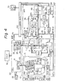
- Figure 4 is a block diagram of another embodiment of a computer system.
- the MPU 10, the BIU 20, the CHIP 30, and the EXT 35 are similar to those in Fig. 1, except that a flag register (FLG-REG) 69 is shown in the EU 6 in a relationship of a MIS 40'.
- the MIS 40' includes a selection circuit (SELECT) 50, a signal mixing circuit (MIX) 51, an a FIFO memory 52, in addition to the MIS 40 shown in Fig. 1, to perform additional instruction surveillance.
- the computer system in Fig. 4 further includes an output buffer (OUT-BUF).
- the SELECT 50 outputs a write command S w or a read command S R to the FIFO memory B 52 in response to the signal S45 at the NAND gate 45.
- the MIX 51 combines an address of bits 11 to 0 on a bus 115 and a flag information of bits 15 to 12 from the FLG-REG 69 in the EU 6.
- the FIFO memory 52 stores the data from the MIX 51, when the signal S w is supplied thereto, or, reads out the data stored therein to the DATA-BUS 100, when the signal S R is supplied thereto, in a FIFO manner.
- FIG. 5 is a view illustrating a data configuration mixed at the MIX 51, accordingly, a view data configuration in the FIFO memory 52.
- Bits 15 to 12 are of flags indicating states of the registers in the MPU 10.
- Bits 11 to 0 are of a microaddress in the MCS 4. From the data shown in Fig. 5, the content of the microinstruction code and the states at the time may be analyzed.
- Data on the DATA-BUS 100 from the FIFO memory 52 is transferred to the OUT-BUF 70 to output them on, for example, a cathode ray tube (CRT) display or a printer (not shown).
- CTR cathode ray tube
- the computer system starts at a time t 0 with a microaddress "000" of a hexadecimal in the MCS 4 and advances microaddresses in accordance with microprogram instructions.
- the signal ACT from the EXT 35 is supplied to the BIU 20.
- the signal BHE of high level and A 0 of high level, indicating "WORD ACCESS ON DEBUG-MODE" as shown in Fig. 3 are supplied to the BIU 20 the MPU 10 through the DATA-BUS 100.
- a signal designating a read cycle is also applied to the BIU 20.
- the BIU 20 interrupts the operation of a microaddress "031" of a hexadecimal and effects an operation "LOAD CONTROL DATA INTO FIFO MEMORY, that is, loading control data as shown in Fig. 9a into the FIFO memory 49. Due to the above operation, eight control data in Fig. 9a are stored in the FIFO memory in the order of Fig. 9a. Each data configuration is as described with reference to Fig. 2. The meaning of the control data will be described later in detail. After completion of the above loading, the normal operation is restored. The operation of the microaddress "031" restarts and subsequent operations are continued.
- the data is a first column in Fig. 9a is loaded into the break point register 41 together with the enable bit of logical "1".
- the IR 1 finds a microprogram instruction of "ADD IMMEDIATE TO GENERAL REGISTER A", which is defined by, for example, a macrocode "803412" in a hexadecimal form shown in Fig. 7 and consists of four microinstruction codes shown in Fig. 8 and stored in the MCS 4, the DEC 3 designates a start microaddress of "050".
- the microinstruction code in the microaddress "050" may be effected in the EU 6.
- the first two parts of the hexadecimal code "80" indicate an operand of the above "ADD IMMEDIATE TO GENERAL REGISTER A”
- the middle two parts of the hexadecimal code "34" a lower address to be loaded into the T-REG aL 63 in the EU 6
- the third two parts of the hexadecimal code "12” an upper address to be loaded into the T-REG aH 63.
- the microinstruction codes shown in Fig. 8 are defined and stored between the microaddresses "050" to "053" in the MCS 4, more specifically, in the region 4a.
- the contents of the microinstruction codes shown in Fig. 8 are as follows:
- the first and second microinstruction codes in the microaddresses "050" and "051" are effected.
- the microaddress "052" is reacted, since the address of "052" and the enable bit of logical "I" as shown in a first column in Fig. 9a were saved in the break point register 41, the operation mode of the computer system is changed to the debug mode, as described before with reference to Fig. 1. Accordingly, the data stored in the FIFO memory 49 and shown in Fig. 9a is supplied to the DEC 3 instead of the data from the MAR 2. Simultaneously, the SELECT 50 outputs the signal Sw to the FIFO memory 52.
- an address "000" in a hexadecimal shown in a second column in Fig. 9a is applied to the MCS 4, and thus an additional instruction stored in the address "000" of the region 4b, shown in Fig. 9b, is effected.
- the first additional instruction is of "transfer a content stored in the T-REG.aL+aH in the EU 6 to the COM-R2 21 in the BIU 2". Due to the execution of the first additional instruction, the content of the T-REG.a 63 is once transferred to the COM-R2 21.
- the COM-R2 21 is connected to the DATA-BUS 100, and thus the content in the COM-R2 21 is transferred on the DATA-BUS 100 and further output through the OUT-BUF 70. Simultaneously, the above address of bits 11 to 0 on the bus 115 and the state flags in the FLG-REG 69 are combined at the MIX 51, and, thus, the same is stored into the FIFO memory 52 from a first address therein. Other additional instructions in addresses between "001" and "011" in the region 4b, corresponding to the control data shown in Fig. 9a, are sequentially effected as similar to the additional instruction of the address "000".
- contents saved in the T-REG.a 63, the T-REG.b 62, the IR 1, and the Ql-REG to Q3-REG 22 to 24, which cannot be accessed by requirements from the programs, and the content in the G-REG.A 65, can be in a visual form through the OUT-BUF 70.
- the last control data shown in Fig. 9a is of bit 13 of logical "1".and bits 15 and 14 of logical "1" indicating "LOAD CONTROL DATA INTO FIFO MEMORY" as shown in Fig. 2. Accordingly, as mentioned above with respect to the operation at the time t 2 , control data (shown in Fig. 9C in this case) are loaded into the FIFO memory 49. Clearly, each control data is defined by the construction shown in Fi g . 2. All control data include a bit of logical "1", thus, the debug mode is still continued. Also, bit 15 is logical "1". In addition, bits 15 and 14 of the last control data is Fig.
- the last control data in Fig. 9C has bits 15 to 13 of logical "1" indicating "RETURN TO NORMAL-MODE OPERATION". Accordingly, after completion of the above control operation for the debugging, the control of the MPU 10 will be restored to the normal mode and the halted microinstruction in an address "053" in the region 4a will start at a time t 7'
- the computer system in Fig. 4 may store addresses from the MAR 2 and flags in the FLG-REG 69 corresponding to the instructions of the addresses into the FIFO memory 52 through the MIX 51 at any time.
- the stored data in the FIFO memory 52 is output through the OUT-BUF 70. This is available for easily testing the operation of the MPU 10.
- Figure 10 is a circuit diagram of still another embodiment of a computer system.
- the MPU 110, the BIU 20, the CHIP 30, and the EXT 35 are basically identical to those in Fig. 1.
- the computer system also includes a MIS 40" and a synchronous-signal application circuit (SAC) 75.
- the MIS 40" includes a break point register 41a which does not include an enable bit, the ENOR 43, the FF 44, an output gate 54, NOR gate 55, and an INV 56.
- An output signal S44 at the FF 44 is connected to the SEQ 5 and the output gate 54 to enable or disable these.
- an output of ENOR 43 is high level, with a result that the FF 44 is reset.
- the signal S44 of high level is supplied to the SEQ 5 and the output gate 54 to ensure the operation of the MPU 10 in the normal-mode operation.
- the FF 44 When the address in the break point register 41a coincides with the address from the MAR 3, the FF 44 is set. Due to the application of the signal S44 of low enable, the operation of the SEQ 5 is halted. Simultaneously, the output gate 54 inhibits passage of the pCODE from the MCS 4 therethrough, with the result that the operation of the microinstruction is compulsorily and temporarily stopped. After a while, upon supply of a synchronous signal S75 at the SAC 75, the FF 44 is reset, restarting the halted microinstruction.
- the generation of the synchronous signal S75 at the SAC 75 may be effected arbitrarily, for example, in response to timing of external equipment jointly operated with the computer system. The restart can also be achieved by applying a RESET signal to the NOR 55.
- the halt can be effected only with every microprogram instruction.
- the halt can be effected not only with every microprogram instruction, but also any microinstruction forming a microprogram instruction.
- the restore of the halt can be effected in response to the synchronization of the other devices.
Landscapes
- Engineering & Computer Science (AREA)
- Software Systems (AREA)
- Theoretical Computer Science (AREA)
- Physics & Mathematics (AREA)
- General Engineering & Computer Science (AREA)
- General Physics & Mathematics (AREA)
- Quality & Reliability (AREA)
- Debugging And Monitoring (AREA)
Applications Claiming Priority (2)
| Application Number | Priority Date | Filing Date | Title |
|---|---|---|---|
| JP60028402A JPS61188626A (ja) | 1985-02-18 | 1985-02-18 | マイクロプロセツサ |
| JP28402/85 | 1985-02-18 |
Publications (2)
| Publication Number | Publication Date |
|---|---|
| EP0194185A2 true EP0194185A2 (fr) | 1986-09-10 |
| EP0194185A3 EP0194185A3 (fr) | 1989-06-07 |
Family
ID=12247667
Family Applications (1)
| Application Number | Title | Priority Date | Filing Date |
|---|---|---|---|
| EP86400332A Ceased EP0194185A3 (fr) | 1985-02-18 | 1986-02-18 | Système d'ordinateur avec configuration de surveillance d'instruction |
Country Status (4)
| Country | Link |
|---|---|
| US (1) | US5129079A (fr) |
| EP (1) | EP0194185A3 (fr) |
| JP (1) | JPS61188626A (fr) |
| KR (1) | KR900000113B1 (fr) |
Cited By (2)
| Publication number | Priority date | Publication date | Assignee | Title |
|---|---|---|---|---|
| US5129079A (en) * | 1985-02-18 | 1992-07-07 | Fujitsu Limited | Computer system having subinstruction surveillance capability |
| EP0473410A3 (en) * | 1990-08-28 | 1993-06-16 | Nec Corporation | Central processing unit |
Families Citing this family (10)
| Publication number | Priority date | Publication date | Assignee | Title |
|---|---|---|---|---|
| JPH06105432B2 (ja) * | 1989-06-01 | 1994-12-21 | 三菱電機株式会社 | マイクロプロセッサ |
| US5469550A (en) * | 1992-01-28 | 1995-11-21 | Cezzar; Ruknet | Reversible computer apparatus and methods of constructing and utilizing same |
| USD361752S (en) | 1993-09-17 | 1995-08-29 | Tokyo Electron Kasbushiki Kaisha | Wafer boat or rack for holding semiconductor wafers |
| US5761467A (en) * | 1993-09-28 | 1998-06-02 | Mitsubishi Denki Kabushiki Kaisha | System for committing execution results when branch conditions coincide with predetermined commit conditions specified in the instruction field |
| JP2630271B2 (ja) * | 1994-09-14 | 1997-07-16 | 日本電気株式会社 | 情報処理装置 |
| US6023564A (en) * | 1996-07-19 | 2000-02-08 | Xilinx, Inc. | Data processing system using a flash reconfigurable logic device as a dynamic execution unit for a sequence of instructions |
| US6915460B2 (en) * | 2001-06-26 | 2005-07-05 | International Business Machines Corporation | Method, apparatus, and program for service processor surveillance with multiple partitions |
| US6452550B1 (en) * | 2001-07-13 | 2002-09-17 | Tyco Electronics Corp. | Reduction of the effects of process misalignment in millimeter wave antennas |
| US7546585B2 (en) * | 2005-01-24 | 2009-06-09 | International Business Machines Corporation | Method, system and computer program product for testing computer programs |
| KR20230069661A (ko) * | 2021-11-12 | 2023-05-19 | 에스케이하이닉스 주식회사 | 메모리 시스템 및 이의 동작 방법 |
Family Cites Families (21)
| Publication number | Priority date | Publication date | Assignee | Title |
|---|---|---|---|---|
| US3898623A (en) * | 1973-06-05 | 1975-08-05 | Ibm | Suspension and restart of input/output operations |
| FR2253435A5 (fr) * | 1973-11-30 | 1975-06-27 | Honeywell Bull Soc Ind | |
| US4205370A (en) * | 1975-04-16 | 1980-05-27 | Honeywell Information Systems Inc. | Trace method and apparatus for use in a data processing system |
| JPS5248440A (en) * | 1975-10-15 | 1977-04-18 | Toshiba Corp | Memory access control system |
| US4240138A (en) * | 1978-10-03 | 1980-12-16 | Texas Instruments Incorporated | System for direct access to a memory associated with a microprocessor |
| US4325121A (en) * | 1978-11-17 | 1982-04-13 | Motorola, Inc. | Two-level control store for microprogrammed data processor |
| JPS5582359A (en) * | 1978-12-18 | 1980-06-21 | Toshiba Corp | Microprogram test unit |
| US4312034A (en) * | 1979-05-21 | 1982-01-19 | Motorola, Inc. | ALU and Condition code control unit for data processor |
| US4338661A (en) * | 1979-05-21 | 1982-07-06 | Motorola, Inc. | Conditional branch unit for microprogrammed data processor |
| US4342078A (en) * | 1979-05-21 | 1982-07-27 | Motorola, Inc. | Instruction register sequence decoder for microprogrammed data processor and method |
| DE2948644A1 (de) * | 1979-12-04 | 1981-06-11 | Robert Bosch Gmbh, 7000 Stuttgart | Vorrichtung zum ueberwachen des inhalts einer speicherzelle eines mikroprozessorsystems |
| IN155448B (fr) * | 1980-03-19 | 1985-02-02 | Int Computers Ltd | |
| US4349873A (en) * | 1980-04-02 | 1982-09-14 | Motorola, Inc. | Microprocessor interrupt processing |
| US4348722A (en) * | 1980-04-03 | 1982-09-07 | Motorola, Inc. | Bus error recognition for microprogrammed data processor |
| US4398244A (en) * | 1980-05-07 | 1983-08-09 | Fairchild Camera & Instrument Corporation | Interruptible microprogram sequencing unit and microprogrammed apparatus utilizing same |
| JPS5886648A (ja) * | 1981-11-18 | 1983-05-24 | Mitsubishi Electric Corp | トレ−ス装置 |
| JPS58109934A (ja) * | 1981-12-23 | 1983-06-30 | Fujitsu Ltd | 処理装置のコンソ−ル |
| JPS593654A (ja) * | 1982-06-30 | 1984-01-10 | Fujitsu Ltd | ヒストリ−メモリ制御方式 |
| DE3241412A1 (de) * | 1982-11-09 | 1984-05-10 | Siemens AG, 1000 Berlin und 8000 München | Vorrichtung zum testen eines hochintegrierten mikroprogramm-gesteuerten elektronischen bauteiles |
| US4635193A (en) * | 1984-06-27 | 1987-01-06 | Motorola, Inc. | Data processor having selective breakpoint capability with minimal overhead |
| JPS61188626A (ja) * | 1985-02-18 | 1986-08-22 | Fujitsu Ltd | マイクロプロセツサ |
-
1985
- 1985-02-18 JP JP60028402A patent/JPS61188626A/ja active Pending
-
1986
- 1986-02-18 KR KR1019860001123A patent/KR900000113B1/ko not_active Expired
- 1986-02-18 EP EP86400332A patent/EP0194185A3/fr not_active Ceased
-
1990
- 1990-10-15 US US07/596,745 patent/US5129079A/en not_active Expired - Lifetime
Cited By (2)
| Publication number | Priority date | Publication date | Assignee | Title |
|---|---|---|---|---|
| US5129079A (en) * | 1985-02-18 | 1992-07-07 | Fujitsu Limited | Computer system having subinstruction surveillance capability |
| EP0473410A3 (en) * | 1990-08-28 | 1993-06-16 | Nec Corporation | Central processing unit |
Also Published As
| Publication number | Publication date |
|---|---|
| JPS61188626A (ja) | 1986-08-22 |
| EP0194185A3 (fr) | 1989-06-07 |
| KR860006732A (ko) | 1986-09-15 |
| US5129079A (en) | 1992-07-07 |
| KR900000113B1 (ko) | 1990-01-20 |
Similar Documents
| Publication | Publication Date | Title |
|---|---|---|
| US4429368A (en) | Microprogram-testing apparatus | |
| KR0168656B1 (ko) | 데이터 처리 시스템 | |
| US5751942A (en) | Trace event detection during trace enable transitions | |
| JP4094724B2 (ja) | ソフトウェアをデバッグする際に例外を識別するための装置および方法 | |
| US5155821A (en) | Command performing order change-over system in data processor | |
| US5129079A (en) | Computer system having subinstruction surveillance capability | |
| US4403287A (en) | Microprocessor architecture having internal access means | |
| US4747045A (en) | Information processing apparatus having an instruction prefetch circuit | |
| US4740895A (en) | Method of and apparatus for external control of computer program flow | |
| WO2009111108A1 (fr) | Procédé et appareil pour partager des ressources de débogage | |
| US3411147A (en) | Apparatus for executing halt instructions in a multi-program processor | |
| JPS5846449A (ja) | コンピユ−タ・プログラムの流れを外部制御する方法および装置 | |
| EP0638864B1 (fr) | Système de support de développement pour microprocesseur à antémémoire interne | |
| US4870573A (en) | Microcomputer capable of testing execution of a program with no branch | |
| US7870434B2 (en) | Method and apparatus for masking debug resources | |
| JPS63173130A (ja) | 計算機の命令セツトを拡張するための装置 | |
| JP2520158B2 (ja) | ディジタルシグナルプロセッサのデバッグ方式 | |
| EP0333613A2 (fr) | Arrêt sur adresse pour mémoire microprogrammable | |
| JPS6248865B2 (fr) | ||
| JPS60193046A (ja) | 命令例外検出方式 | |
| JPS63307543A (ja) | デバッグ装置 | |
| JPS63155330A (ja) | マイクロプログラム制御装置 | |
| JPS6238746B2 (fr) | ||
| JPS6091458A (ja) | マイクロプロセツサのプログラムデバツグ装置 | |
| JPH04367902A (ja) | プログラマブルコントローラ |
Legal Events
| Date | Code | Title | Description |
|---|---|---|---|
| PUAI | Public reference made under article 153(3) epc to a published international application that has entered the european phase |
Free format text: ORIGINAL CODE: 0009012 |
|
| AK | Designated contracting states |
Kind code of ref document: A2 Designated state(s): DE FR GB |
|
| PUAL | Search report despatched |
Free format text: ORIGINAL CODE: 0009013 |
|
| AK | Designated contracting states |
Kind code of ref document: A3 Designated state(s): DE FR GB |
|
| 17P | Request for examination filed |
Effective date: 19891125 |
|
| 17Q | First examination report despatched |
Effective date: 19920311 |
|
| STAA | Information on the status of an ep patent application or granted ep patent |
Free format text: STATUS: THE APPLICATION HAS BEEN REFUSED |
|
| 18R | Application refused |
Effective date: 19940611 |
|
| RIN1 | Information on inventor provided before grant (corrected) |
Inventor name: MIYASHITA, TAKUMI |