EP0196540A1 - Visualisation de formes d'onde de données numériques - Google Patents
Visualisation de formes d'onde de données numériques Download PDFInfo
- Publication number
- EP0196540A1 EP0196540A1 EP86103611A EP86103611A EP0196540A1 EP 0196540 A1 EP0196540 A1 EP 0196540A1 EP 86103611 A EP86103611 A EP 86103611A EP 86103611 A EP86103611 A EP 86103611A EP 0196540 A1 EP0196540 A1 EP 0196540A1
- Authority
- EP
- European Patent Office
- Prior art keywords
- data
- state
- waveform
- character
- display
- Prior art date
- Legal status (The legal status is an assumption and is not a legal conclusion. Google has not performed a legal analysis and makes no representation as to the accuracy of the status listed.)
- Withdrawn
Links
Images


Classifications
-
- G—PHYSICS
- G01—MEASURING; TESTING
- G01R—MEASURING ELECTRIC VARIABLES; MEASURING MAGNETIC VARIABLES
- G01R13/00—Arrangements for displaying electric variables or waveforms
- G01R13/20—Cathode-ray oscilloscopes
- G01R13/22—Circuits therefor
-
- G—PHYSICS
- G01—MEASURING; TESTING
- G01R—MEASURING ELECTRIC VARIABLES; MEASURING MAGNETIC VARIABLES
- G01R31/00—Arrangements for testing electric properties; Arrangements for locating electric faults; Arrangements for electrical testing characterised by what is being tested not provided for elsewhere
- G01R31/28—Testing of electronic circuits, e.g. by signal tracer
- G01R31/317—Testing of digital circuits
- G01R31/3177—Testing of logic operation, e.g. by logic analysers
-
- G—PHYSICS
- G06—COMPUTING OR CALCULATING; COUNTING
- G06F—ELECTRIC DIGITAL DATA PROCESSING
- G06F11/00—Error detection; Error correction; Monitoring
- G06F11/22—Detection or location of defective computer hardware by testing during standby operation or during idle time, e.g. start-up testing
- G06F11/25—Testing of logic operation, e.g. by logic analysers
Definitions
- the present invention relates to devices for acquiring and storing digital data representing waveforms and in particular to a method and apparatus for compactly displaying such acquired and stored data.
- RAM random access memory
- Logic analyzers have typically reproduced the sampled waveforms on a screen in graphical form. As the detail and the length of the waveforms stored in memory have increased, simple reproduction of an entire stored waveform is not possible, even with the use of large, high resolution screens.
- Use of state displays has allowed acquired waveform information to be more compactly displayed. In a state display, the state of a waveform or a set of waveforms is represented by a number displayed at each sampling interval.
- waveform data acquired by a logic analyzer from one or more digital channels is displayed on a screen as a busform, wherein a change of state in any of the channels during a sampling interval is represented by a solid block character on the screen, and wherein the lack of a change of state in any of the channels during a sampling interval is represented by a space character of the same width as the block character.
- the blocks and spaces representing contiguous sampling intervals are displayed in horizontal sequence across the screen such that the time between state changes is graphically represented by the horizontal distance between the blocks. Since waveform data is often represented in manufacturer's literature in a similar form, many operators are familiar with, and have an intuitive understanding of, this method of waveform representation. Moreover, the display of waveform data as a busform permits the operator to correlate easily the acquired data with manufacturer's specifications.
- means are provided to compress the display by displaying a block on the screen whenever one or more changes of state occur during a selected number of sampling periods and by displaying a space whenever no changes of state occurs during the same number of sampling periods. This allows the operator to view a longer portion of the busform on the screen.
- means are provided to expand the busform display to permit an operator to display a smaller portion of a busform on the screen in greater detail.
- data representing the associated waveform state is displayed when possible in the space or spaces following each block character.
- a waveform display circuit illustrated in block diagram form is adapted to generate a busform display of acquired waveform data associated with one or more sampled waveforms in accordance with a preferred embodiment of the present invention.
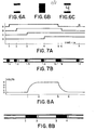
- FIG. 7A Four such waveforms, designated A, B, C and D, are depicted in graphical form in FIG. 7A.
- the waveforms are sampled by a logic analyzer (not shown) at regular time intervals.
- a binary state number representing the collective state of the four waveforms is stored in a random access acquisition memory 10, with state numbers for successive sampling intervals being stored at successive acquisition memory 10 addresses.
- the state number to be stored is a 4-bit binary number wherein the state (0 or 1) of waveform A is the least significant bit, the state of waveform D is the most significant bit, and the states of waveforms B and C are the next least significant bits, respectively.
- the state number may take on any value from 0000 to 1111 (0 to F in hexadecimal form). For example, in FIG. 7A, prior to time 1 the state number is 0000, while between time 1 and time 2, the state number stored is 0001. Similarly, between times 2 and 3 the state number is 0011, and after time 7 the state number is 1100.
- the logic analyzer apparatus required for sampling the waveforms, and calculating and storing the state numbers, is well known in the art and is not further detailed herein.
- the stored state number data is displayed on cathode ray tube (CRT) screen 26, of FIG. 1 in a busform graphical representation wherein a change of state number during a given time interval (display period) is represented by a block character, such as that shown in FIG. 6B, while the lack of a change of state number during a display period is represented by a space character, such as depicted in FIG. 6A.
- FIG. 7B is a typical diagram of a busform display of the waveforms of FIG. 7A, according to the present invention. State changes occurring at times 1 to 6 in FIG. 7A are represented by corresponding block characters 1 to 6 of FIG.
- waveform A changed state several times in rapid succession during one display period immediately prior to time 7.
- the block at position 7 indicates that at least one state change has occurred during the previous display period, but since the display period is larger than the period used to sample the waveforms, in the example shown, block characters indicating each of the state changes occurring during the period of rapid state changes in waveform A immediately prior to time 7 are not separately displayed in the busform of FIG. 7B.
- the display period may be shortened to allow for separate display of block characters associated with each state change in the period immediately preceding time 7. Further, as also described hereinbelow, the display period may be increased (thereby decreasing the display resolution) such that the waveform data is further compressed, thereby allowing longer portions of waveforms to be characterized by a busform on a screen.
- the hexidecimal equivalent of the state numbers associated with the waveforms, during the periods between state changes, are displayed superimposed over the corresponding space characters following each block, whenever there are sufficient such space characters to do so.
- An example of such superposition is shown in FIG. 6C.
- the block character represents the state change at time 3 of FIG. 7A
- the number 7 following the third block character represents the state number 1100 (binary) of the lines between times 3 and 4.
- No state number is displayed following the block at position 5 of FIG. 7B because there is insufficient space between blocks at positions 5 and 6 to do so.
- the number C following the block character at position 7 indicates the state of the waveforms after the last change of state immediately preceding time 7. While the preferred embodiment of the present invention provides for display of only single hexidecimal character state numbers as shown in FIG 7B, state numbers or other data descriptive of the state of the sampled waveforms consisting of more than one digit and in other than hexidecimal form may be displayed in alternative embodiments.
- acquisition memory 10 is sequentially addressed by an accumulator 12.
- Accumulator 12 adds the contents of an increment register 14 to a stored number each time accumulator 12 detects a pulse (CLK) from a system clock (not shown). Initially, the number stored by accumulator 12 is set to zero by an externally generated RESET signal.
- acquisition memory 10 is a 64K (65,536) byte memory, capable of storing a 4 bit state number at each memory location, and that accumulator 12 is capable of storing a 24 bit number, with the upper 16 bits being used to address acquisition memory 10
- increment register 14 contains a binary 1 the contents of accumulator 12 will increase by 1 each time the accumulator is strobed by a CLK pulse. Every 256 times the accumulator 12 increments by 1, the current address of acquisition memory 10 increments by 1 and the binary state number stored at the current address occurs on four data output lines 16 of acquisition memory 10.
- the binary increment register 14 contains the binary number 256, then the number stored by accumulator 12 increases by 256 and the current address of acquisition memory 10 is incremented by one on occurrence of each CLK pulse.
- Data output lines 16 from acquisition memory 10 are applied in parallel to a maximum detector 18 and a minimum detector 20.
- Maximum detector 18 compares the value of the current state number on lines 16 with the value of an internally stored number and replaces the stored number with the currently addressed state number if it is larger than the stored number.
- minimum detector 20 compares the value of the current state number on lines 16 with the value of a stored number and replaces the stored number with the current state number if it is smaller than the stored number.
- the stored number in the maximum detector 18 is reset to 0000 on each occurrence of a pulse on applied STEP,control line indicating the start of a new display period.
- the number stored by the minimum detector is reset to 1111 on receipt of a STEP pulse.
- maximum detector 18 stores the largest state number outputted by acquisition memory 10 during a display period between STEP pulses
- minimum detector 20 stores the smallest state number outputted by acquisition memory 10 during a display period.
- comparator 22 The numbers stored by maximum detector 18 and minimum detector 20 are transmitted to the A and B inputs of comparator 22.
- Comparator 22 produces a high logic level output signal whenever the A and B inputs are dissimilar and a low logic level signal whenever the A and B inputs are similar.
- the output of comparator 22 is applied to a character table 24 which generates binary numbers representing the graphical characters block and space forming the busform to be displayed on screen 26. If the output of comparator 22 is low, then character table 24 will output a number representing the graphical space character depicted in FIG. 6A, while if the output of comparator 22 is high, character table 24 will output a number representing the graphical block character depicted in FIG. 6B.
- Character table 24 may be a read only memory with the data from comparator 22 being applied to the address inputs of the memory and the graphical character numbers being generated at the data output terminals of the memory. Each memory location of character table 24 addressed by comparator 22 may be preloaded with whatever data may be required by display driver 44 to produce the appropriate graphical character on screen 26.
- the output of character table 24 is applied to one input channel of a multiplexer 28.
- the binary state number stored by minimum detector 20 is converted by a second character table 30 (which may be similar to character table 24) to a corresponding character code to be used in displaying the state number superimposed on a space character on screen 26, as illustrated in FIG. 6C.
- the converted state number is then applied to a second input channel of multiplexer 28.
- the output of multiplexer 28, equivalent to the data input from either character table 24 or 30 depending on the switching state of multiplexer 28, is connected to the data input terminals of a random access display memory 32 such that the transmitted data is stored at the currently addressed display memory location whenever the write control of display memory 32 is strobed by a STEP pulse.
- a multiplexer control circuit 34 monitors the output of comparator 22 and determines if there is a display period between two STEP pulses wherein there is no change of state immediately following a display period wherein there has been a change of state. If there is such a period of quiescence following a display period of state change, then control circuit 34 causes multiplexer 28 to pass the data from circuit 30 to display memory 32 during the quiescent period. At all other times control circuit 34 causes multiplexer 28 to pass the data from character table 24 to the data inputs of display memory 32.
- Boundary detector 36 monitors the current address of acquisition memory 10 and produces a high logic level output signal whenever the current address falls within stored limits. This output signal is also applied to an address line of character table 24, along with the output signal of comparator 22. If the output signal of boundary detector 36 is not in a high state, then the data output of character table 24 represents a blank space to be ignored by display driver 44 in creating the busform display on screen 26. If the output signal of boundary detector 36 is in a low logic level state, then the output of character table 24 will be determined by the state of the output of comparator 22 as described hereinabove. Thus the limit data stored in boundary detector 36 controls the beginning and ending point of the busform display on screen 26.
- Display memory 32 is sequentially addressed by an accumulator 38 which adds the contents of an increment register 40 to a stored number each time accumulator 38 detects a pulse (CLK) from the system clock. Initially, the number stored by accumulator 12 is set to zero by an externally generated RESET signal. Assuming, by way of example, that display memory 10 is a 64K byte random access memory capable of storing one character data number at each memory location, accumulator 12 may be capable of storing a 24 bit binary number, with the upper 16 bits being used to address display memory 32.
- increment register 40 contains a binary 1
- the contents of accumulator 38 will increase by 1 each time the accumulator is strobed by a CLK pulse and the current address of display memory 32 will increase by 1 for every 256 CLK pulses.
- display memory 32 receives a STEP pulse at its write strobe input terminal, the data from multiplexer 28 is written into the current memory location.
- Step detector 42 monitors the least significant bit of the address lines leading to display memory 32 from accumulator 38 and generates a STEP pulse each time the least significant bit changes state.
- the STEP pulses define the beginning and end of each display period, and any block or space character displayed in the busform on screen 26 represents the state change behavior of all of the sampled waveforms during a single display period.
- the STEP pulse is applied to the write strobe input of display memory 32 to initiate a write operation, and to minimum detector 20, maximum detector 18 and multiplexer control circuit 34 to indicate the beginning of a new display period.
- display memory 32 The contents of display memory 32 are accessed by a suitably configured display driver circuit 44 and used as a basis to generate a busform display on screen 26.
- a suitably configured display driver circuit 44 Circuits capable of performing the function of display driver circuit 44 are well known in the art and are not further detailed herein.
- a more detailed embodiment of boundary detector 36 of FIG. 1, shown in block diagram form in FIG. 2, comprises a high address register 46, a low address register 48, comparators 50 and 52, and an AND gate 54.
- high register 46 is loaded with the 16 bit address of the last waveform sample data in acquisition memory 10 to be displayed on the screen
- low address register 48 is loaded with the address of the first waveform sample data to be represented on the screen.
- the data stored in register 46 is transmitted to the A input terminal of comparator 50 while the data stored by register 48 is applied to the B input of comparator 52.
- the address data from accumulator 12 is applied to the B input of comparator 50 and to the A input of comparator 52.
- Comparators 50 and 52 each produce a high logic level output when the value of the A input exceeds the value of the B input.
- the outputs of comparators 50 and 52 are connected to AND gate 54 such that the output of AND gate 54 is high only when the current address of acquisition memory 10 falls between the values stored in registers 46 and 48. This AND gate 54 output is then applied to character table 24 of FIG. 1.
- a more detailed embodiment of maximum detector 18 of FIG. 1, depicted in block diagram form in FIG. 3, comprises a comparator 56 and a maximum register ' 58.
- the state number contained at the current acquisition memory 10 address is applied to a B input of comparator 56 and to the data input terminals of register 58, while the number stored by maximum register 58 is applied to an A input of comparator 56.
- the output of comparator 56 connected to a load control input of register 58, is high if the B input exceeds the A input.
- the load control input of register 58 is driven high, the contents of register 58 are replaced by the current state number. This happens whenever the current state number is higher than any previously stored state number.
- Register 58 is reset to zero upon receipt of a STEP pulse.
- the number stored by register 58 at the time of reset is equal to the highest state number appearing at the data output terminal of acquisition memory 10 during the previous display period.
- a more detailed embodiment of minimum detector 20 of FIG. 1, depicted in block diagram form in FIG. 4, comprises a comparator 60 and a minimum register 62.
- the state number contained at the current acquisition memory 10 address is applied to a B input of comparator 60, and to the data input terminal of register 62, while the number stored by minimum register 62 is applied to an A input of comparator 60.
- the output of comparator 60 connected to a load control input of register 62, is high if the A input exceeds the B input.
- Register 62 is reset to a maximum upon receipt of a STEP pulse. Thereafter the contents of register 62 are replaced by the current state number whenever the current state number is lower than any previously stored number.
- the number stored by register 62 just prior to reset is equal to the lowest state number appearipg at the data output terminal of acquisition memory 10 during the previous display period.
- multiplexer circuit 34 of FIG. 1 is shown in more detail in FIG. 5 in block diagram form.
- multiplexer circuit 34 comprises a D type flip-flop 64 which stores the current state of the output of comparator 22 each time it receives a STEP pulse.
- the output state of terminal Q of flip-flop 64 controls the state of a non-inverting input to an AND gate 66 while the output of comparator 22 controls the state of an inverting input to AND gate 66.
- the output of AND gate 66 controls the switching state of multiplexer 28.
- the output of circuit 22 remains low. If no change of state of the sampled waveform occurs during the previous display period, the Q output of flip-flop 66 will be low, causing the output of AND gate 66 to remain low regardless of the state of the output of circuit 22. Only if flip-flop 64 is set, the high Q output indicating a change of state of sampled waveform occurred during the previous display period, and if the output of circuit 22 is low, indicating no change of sampled waveform state during the current display period, will the output of AND gate 66 be high, thereby causing multiplexer 28 to couple the output of character table 30 to display memory 32.
- the multiplexer control circuit causes display memory 32 to store the state number only during the first display period after a sampled waveform state change, and only if no subsequent state change occurs during that display cycle.
- acquisition memory 10 is loaded with the appropriate waveform data while the high and low registers of boundary detector 36 are loaded with the acquisition memory addresses of the first and last data points to be displayed in the busform on screen 26.
- Increment register 14 is loaded with a number from 1 to 255 to control the number of CLK pulses required to increment the current address of acquisition memory 10.
- increment register 40 is loaded with another number from 1 to 255 to control the number of CLK pulses required to increment the current address of display memory 32..
- increment register 14 contains a small number, then the address of acquisition memory 10 is incremented less often with respect to the frequency of the system CLK pulses and less often with respect to the frequency of the STEP pulses which control the rate of data storage in display memory 32.
- relatively fewer waveform sample points in acquisition memory 10 are applied to maximum detector 18 and minimum detector 20 between any two STEP pulses. Therefore the data stored in display memory 32 on occurrence of each STEP represents the change of state behavior of the sampled waveforms over relatively fewer sample points. It follows that by decreasing the size of the number stored in increment register 14, the busform display is expanded, showing more state change detail.
- increment register 40 the more compressed is the busform display, with the state change behavior of more successive sample points in acquisition memory 10 being lumped into a single representative busform character on screen 26.
- accumulator 38 requires more CLK pulses to increment display memory 32 and step detector 42 produces STEP pulses less often. The less frequent STEP pulses cause maximum and minimum detectors 18 and 20 to reset less often such that more successive waveform sample points are received and evaluated by maximum and minimum detectors 18 and 20 between each resetting.
- an operator may want to set the high and low address numbers in boundary detector 36 widely spaced so that a long portion of a sampled wave form will be characterized by the busform on screen 26.
- the operator would set the number in increment register 14 relatively high and the number in increment register 40 relatively low, such that the busform will be highly compressed. Because the resulting busform would be compressed, comparatively little detail of the waveform activity would be apparent. Fewer state numbers may be displayed due to the lack of sufficient display space following state change indicators, but periods of high state change activity could be distinguished from periods of low state change activity and gross changes in state change patterns could be distinguished.
- the operator could then check sections of the busform in increasing detail by setting narrower limits in boundary detector 36, lower numbers in increment register 14 and higher numbers in increment register 40. At the highest level of detail, every state change during a small portion of the sampled waveforms will be separately represented by a state change character in the busform display, and there will be sufficient space following every state change character to display the state number.
- sample data stored in acquisition memory 10 has been sample data associated with digital waveforms as depicted in FIG. 7A
- sample data may also represent a sampled analog waveform as seen in FIG. 8A, where the data stored in acquisition memory 10 represents the voltage magnitude of the analog waveform at each sampled point.
- a busform such as might be produced by the circuit of FIG. 1 from such stored sample data is shown in FIG. 8B. Periods of change in waveform magnitude would appear in the busform as a solid string of state change characters followed by a state number representing the voltage of the waveform at the end of the change. No modification to the circuit of FIG. 1 is necessary to produce such a busform from such analog waveform sample data.
Landscapes
- Engineering & Computer Science (AREA)
- Physics & Mathematics (AREA)
- General Physics & Mathematics (AREA)
- General Engineering & Computer Science (AREA)
- Theoretical Computer Science (AREA)
- Computer Hardware Design (AREA)
- Quality & Reliability (AREA)
- Controls And Circuits For Display Device (AREA)
Applications Claiming Priority (2)
| Application Number | Priority Date | Filing Date | Title |
|---|---|---|---|
| US713137 | 1985-03-18 | ||
| US06/713,137 US4673931A (en) | 1985-03-18 | 1985-03-18 | Waveform data display |
Publications (1)
| Publication Number | Publication Date |
|---|---|
| EP0196540A1 true EP0196540A1 (fr) | 1986-10-08 |
Family
ID=24864893
Family Applications (1)
| Application Number | Title | Priority Date | Filing Date |
|---|---|---|---|
| EP86103611A Withdrawn EP0196540A1 (fr) | 1985-03-18 | 1986-03-18 | Visualisation de formes d'onde de données numériques |
Country Status (3)
| Country | Link |
|---|---|
| US (1) | US4673931A (fr) |
| EP (1) | EP0196540A1 (fr) |
| JP (1) | JPS61219870A (fr) |
Cited By (1)
| Publication number | Priority date | Publication date | Assignee | Title |
|---|---|---|---|---|
| EP0245915A3 (fr) * | 1986-05-02 | 1989-11-29 | Tektronix, Inc. | Affichage d'états et de temps de signaux logiques |
Families Citing this family (10)
| Publication number | Priority date | Publication date | Assignee | Title |
|---|---|---|---|---|
| JPS61270666A (ja) * | 1985-05-25 | 1986-11-29 | Sony Corp | デイジタルデ−タの表示方法 |
| US4777616A (en) * | 1986-05-12 | 1988-10-11 | Outlook Technology, Inc. | Increased resolution logic analyzer using asynchronous sampling |
| US4818932A (en) * | 1986-09-25 | 1989-04-04 | Tektronix, Inc. | Concurrent memory access system |
| US4977514A (en) * | 1987-05-08 | 1990-12-11 | Hewlett Packard Company | Overlaid digital waveforms display |
| US5091721A (en) * | 1988-12-22 | 1992-02-25 | Hughes Aircraft Company | Acoustic display generator |
| JPH087240B2 (ja) * | 1989-03-08 | 1996-01-29 | 富士通株式会社 | 波形表示方法 |
| JPH05322931A (ja) * | 1992-05-18 | 1993-12-07 | Toyo Tekunika:Kk | ロジックアナライザ |
| JP4941725B2 (ja) * | 2007-01-11 | 2012-05-30 | 横河電機株式会社 | 波形測定装置 |
| JP4924882B2 (ja) * | 2007-01-30 | 2012-04-25 | 横河電機株式会社 | 波形測定装置 |
| JP7717443B2 (ja) * | 2020-04-24 | 2025-08-04 | 横河電機株式会社 | デジタルオシロスコープ |
Citations (2)
| Publication number | Priority date | Publication date | Assignee | Title |
|---|---|---|---|---|
| FR2514900A1 (fr) * | 1981-10-08 | 1983-04-22 | Tektronix Inc | Dispositif de memorisation et de visualisation de formes d'onde |
| US4493044A (en) * | 1982-03-08 | 1985-01-08 | Tektronix | Apparatus and a method of establishing the correct display order of probe channels for a logic analyzer |
Family Cites Families (9)
| Publication number | Priority date | Publication date | Assignee | Title |
|---|---|---|---|---|
| JPS5813864B2 (ja) * | 1979-11-26 | 1983-03-16 | 岩崎通信機株式会社 | ロジツク信号観測装置 |
| US4455558A (en) * | 1981-05-06 | 1984-06-19 | Williams Jr Albert J | Combined analog digital symbols |
| JPS5866865A (ja) * | 1981-10-17 | 1983-04-21 | Iwatsu Electric Co Ltd | 信号観測装置 |
| JPS58105067A (ja) * | 1981-12-17 | 1983-06-22 | Sony Tektronix Corp | 表示装置 |
| JPS58140899A (ja) * | 1982-02-16 | 1983-08-20 | ソニ−・テクトロニクス株式会社 | ロジツク信号表示方法 |
| EP0094976B1 (fr) * | 1982-05-24 | 1986-08-27 | Ibm Deutschland Gmbh | Analyseur logique |
| US4536760A (en) * | 1982-10-15 | 1985-08-20 | Tektronix, Inc. | Signal-envelope display system for a digital oscilloscope |
| US4554536A (en) * | 1983-03-23 | 1985-11-19 | Tektronix, Inc. | Logic timing diagram display apparatus |
| US4560981A (en) * | 1983-03-23 | 1985-12-24 | Tektronix, Inc. | Logic waveform display apparatus |
-
1985
- 1985-03-18 US US06/713,137 patent/US4673931A/en not_active Expired - Fee Related
-
1986
- 1986-03-18 JP JP61060483A patent/JPS61219870A/ja active Pending
- 1986-03-18 EP EP86103611A patent/EP0196540A1/fr not_active Withdrawn
Patent Citations (2)
| Publication number | Priority date | Publication date | Assignee | Title |
|---|---|---|---|---|
| FR2514900A1 (fr) * | 1981-10-08 | 1983-04-22 | Tektronix Inc | Dispositif de memorisation et de visualisation de formes d'onde |
| US4493044A (en) * | 1982-03-08 | 1985-01-08 | Tektronix | Apparatus and a method of establishing the correct display order of probe channels for a logic analyzer |
Cited By (1)
| Publication number | Priority date | Publication date | Assignee | Title |
|---|---|---|---|---|
| EP0245915A3 (fr) * | 1986-05-02 | 1989-11-29 | Tektronix, Inc. | Affichage d'états et de temps de signaux logiques |
Also Published As
| Publication number | Publication date |
|---|---|
| JPS61219870A (ja) | 1986-09-30 |
| US4673931A (en) | 1987-06-16 |
Similar Documents
| Publication | Publication Date | Title |
|---|---|---|
| US4495586A (en) | Waveform acquisition apparatus and method | |
| US4907176A (en) | Flag generation system | |
| US4510571A (en) | Waveform storage and display system | |
| US4283713A (en) | Waveform acquisition circuit | |
| US4673931A (en) | Waveform data display | |
| US4835675A (en) | Memory unit for data tracing | |
| EP0159588B1 (fr) | Analyseur logique | |
| US4876655A (en) | Method and apparatus for evaluating jitter | |
| EP0901636A1 (fr) | Ecran d'oscilloscope numerique et procede afferent | |
| US5115404A (en) | Digital storage oscilloscope with indication of aliased display | |
| US4536760A (en) | Signal-envelope display system for a digital oscilloscope | |
| JPH0131143B2 (fr) | ||
| US4906916A (en) | Signal processing device having high speed shift register | |
| US4251814A (en) | Time dot display for a digital oscilloscope | |
| US4755960A (en) | Waveform data compressing circuit | |
| US4516119A (en) | Logic signal display apparatus | |
| US4608652A (en) | Method of displaying a logic signal | |
| DE69112479T2 (de) | Test und Messinstrument mit digitaler Speicherung. | |
| US4560981A (en) | Logic waveform display apparatus | |
| CA1151329A (fr) | Methode d'affichage de signaux logiques pour appareil de mesure de signaux logiques | |
| EP0245915A2 (fr) | Affichage d'états et de temps de signaux logiques | |
| EP0225704A2 (fr) | Méthode et appareil pour faire l'analyse de la forme d'une onde | |
| JPS63277975A (ja) | トリガー事象捕促装置 | |
| US4903219A (en) | Method of identifying flag bits | |
| GB2059229A (en) | Signal-envelope display system for a digital oscilloscope |
Legal Events
| Date | Code | Title | Description |
|---|---|---|---|
| PUAI | Public reference made under article 153(3) epc to a published international application that has entered the european phase |
Free format text: ORIGINAL CODE: 0009012 |
|
| AK | Designated contracting states |
Kind code of ref document: A1 Designated state(s): DE FR GB NL |
|
| 17P | Request for examination filed |
Effective date: 19861111 |
|
| 17Q | First examination report despatched |
Effective date: 19880830 |
|
| STAA | Information on the status of an ep patent application or granted ep patent |
Free format text: STATUS: THE APPLICATION IS DEEMED TO BE WITHDRAWN |
|
| 18D | Application deemed to be withdrawn |
Effective date: 19890110 |
|
| RIN1 | Information on inventor provided before grant (corrected) |
Inventor name: CUNNINGHAM, HOWARD G. |