EP0199458A2 - Circuit de mémoire ayant un schéma d'écriture - Google Patents
Circuit de mémoire ayant un schéma d'écriture Download PDFInfo
- Publication number
- EP0199458A2 EP0199458A2 EP86301978A EP86301978A EP0199458A2 EP 0199458 A2 EP0199458 A2 EP 0199458A2 EP 86301978 A EP86301978 A EP 86301978A EP 86301978 A EP86301978 A EP 86301978A EP 0199458 A2 EP0199458 A2 EP 0199458A2
- Authority
- EP
- European Patent Office
- Prior art keywords
- bit lines
- period
- lines
- control signal
- circuit
- Prior art date
- Legal status (The legal status is an assumption and is not a legal conclusion. Google has not performed a legal analysis and makes no representation as to the accuracy of the status listed.)
- Granted
Links
Images


Classifications
-
- G—PHYSICS
- G11—INFORMATION STORAGE
- G11C—STATIC STORES
- G11C7/00—Arrangements for writing information into, or reading information out from, a digital store
- G11C7/10—Input/output [I/O] data interface arrangements, e.g. I/O data control circuits, I/O data buffers
- G11C7/1078—Data input circuits, e.g. write amplifiers, data input buffers, data input registers, data input level conversion circuits
- G11C7/1084—Data input buffers, e.g. comprising level conversion circuits, circuits for adapting load
-
- G—PHYSICS
- G11—INFORMATION STORAGE
- G11C—STATIC STORES
- G11C7/00—Arrangements for writing information into, or reading information out from, a digital store
-
- G—PHYSICS
- G11—INFORMATION STORAGE
- G11C—STATIC STORES
- G11C7/00—Arrangements for writing information into, or reading information out from, a digital store
- G11C7/10—Input/output [I/O] data interface arrangements, e.g. I/O data control circuits, I/O data buffers
- G11C7/1078—Data input circuits, e.g. write amplifiers, data input buffers, data input registers, data input level conversion circuits
Definitions
- the present invention relates to a memory circuit, and particularly to a static type random access memory (SRAM) comprised of MOS field effect transistors (MOSFETs).
- SRAM static type random access memory
- MOSFETs MOS field effect transistors
- SRAMs have been widely utilized in various fields as high speed RAMs.
- a so-called internal-synchronous SRAM has been proposed and presently subjected to practical use.
- the internal-synchronous SRAM when a change in address inputs occurs for a new access cycle, at least one control signal is generated within a SRAM and the new access cycle is initiated under control of the above at least one control signal.
- a precharge signal is first generated so that each pair of bit lines are precharged.
- read signals on each pair of bit lines are amplified by a sense amplifier.
- a column enable signal is generated and a selected pair of bit lines are connected to a pair of bus lines. Then, data on the bus lines is outputted by an output circuit.
- the precharge of bit lines, the selection of word lines are sequentially conducted as in the case of a reading operation. While in this case, a write control signal is activated at the same time as the selection of the word lines so that an input buffer is enabled.
- the input buffer circuit generates the input data on the pair of bus lines after a relatively short time has elapsed from the enable of the input buffer.
- the selective connection of a pair of bit lines to the pair of bus lines is conducted after a relatively large time has elapsed from the selection of word lines as in the case of the read operation. Namely, the timing relation from the change in address inputs to the selection of bit lines in the write operation is fixed in the same manner as in the read operation.
- the memory circuit according to the present invention is of the type having a plurality of word lines, a plurality of bit lines, a plurality of memory cells coupled to the word lines and the bit lines, a bus line, a bit line selection circuit for performing data transfer between the selected bit line and the bus line, and an input data buffer for operatively supplying the bus line with input data, the bit line selection circuit being enabled by a first control signal which is generated when a first time period has elapsed from the initiation of an access cycle, the input buffer circuit being enabled by a second control signal which is generated when a second time period has elapsed from the initiation of the access cycle in a write mode, the second period being shorter than the first period, and is featured in that the bit line selection circuit is adapted to be enabled in response to either one of the first and second control signals in a write mode.
- the bit line selection circuit is enabled by the second control circuit at an earlier time than the enabling of the bit line selection circuit by the first control signal. Accordingly, a fast write operation can be conducted.
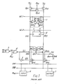
- P-channel field effect transistors Qp 1 to Qp 3 form a bit line precharge circuit for precharging a pair of bit lines DG1 and DCl in response to a low level of a precharge control signal 0 p i .
- a memory cell 1 connected to the pair of bit lines DG1 and Yj1 and a word line WL,.
- the memory cell 1 is composed of N-channel field effect transistors Q N1 to Q N4 and load resistors R, and R 2 . Other memory cells such as 2 have the same configuration.
- N-channel field effect transistors Q NS to Q N7 form a sense amplifier for the pair of bit lines DG and DG .
- a common node N 4 is connected to the sources of the transistors Q N7 of the respective sense amplifiers.
- a sense enable transistor Q N8 of N-channel is connected between the node N 4 and a ground potential.
- the transistor Q N8 enables the selected sense amplifier in response to a high (V cc ) level of a sense enable signal ⁇ R1.
- the bit line DG1 is connected through a parallel circuit of an N-channel transistor Q N9 and a P-channel transistor Q P4 to a bus line DB1, while the bit line DB1 is connected to a bus line DB1 via a parallel circuit of an N-channel transistor Q N10 and P-channel transistor Q p5 .
- a NAND gate 3 receiving address input signals A o to A n serves as a column address decoder, and a NOR gate 4 receiving the output N5 of the gate 3 and a column enable signal ⁇ Yi for operatively performing a column selection by way of its output Y j1 and its inverted output y j1 via an inverter 5.
- An output circuit 7 is connected to the but lines DB1 and DB1 . The output circuit 7 generates an output signal at an output terminal OUT.
- An input circuit 6 coupled to the bus lines DB1 and DB1 applies an input data at an input terminal IN to the bus lines DB1 and DB1 in response to a write enable signal ⁇ WE1 .
- the read operation is explained.
- a time point t at least one address input signal is changed and a new access cycle is initiated.
- the precharge control signal ⁇ P1 falls in level between time points t2 and t 3 so that the pair of bit lines DG1 and DB1 are precharged during this period (t 2 -t3).
- one of the word lines e.g. WL2 is selected. Therefore, the levels of the pair of bit lines DG1 and DB1 start to change according to memory contend of the selected memory cell.
- the column enable signal ⁇ Yj falls in level thereby to determine the state of the column selection signals Y J1 and Yj1 . If the column of DG1, is selected by "1" level of Yj1 and "0" level of Yj1 the sense amplifier provided for this column (DG1, Yj1 ) is enabled to enlarge the potential difference between the bit lines DG1 and Yj1 .
- the pair of bus lines DB1 and D &1 are connected to the selected bit lines DG1 and Yj1 , and hence the potentials on the bus lines DB1 and Yj1 are also amplified by the sense amplifier.
- the amplified signals on the bus lines are inputted to the output circuit 7 for a read-out signal.
- a certain period ⁇ t is provided between t 3 and t 4 .
- the sense amplifier is not enabled.
- the bit lines DG1 and Yj1 are connected to DB1 and DB1 via transistors Q N9 and Qp 4 and Q N10 and Q P5 , respectively.
- the input data is transmitted to the selected bit lines DG1 and DG1 achieving the write operation.
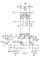
- FIG. 3 a memory according to one embodiment of the invention is explained.
- This embodiment newly comprises an inverter 11 receiving the column enable signal ⁇ Yj , identical to ⁇ Yj in Fig. 1, to generate an inverted signal Oyj and a NOR gate 10 receiving Oyj and the write control signal ⁇ WE1 .
- An output ⁇ YjWE of the NOR gate 10 is inputted to the NOR gate 4 in place of ⁇ Yj in Fig. 1.
- the write control signal ⁇ WE1 upon a read operation the write control signal ⁇ WE1 is at a low level and hence the signal ⁇ YjWE assumes the same level as the signal ⁇ Yj . Therefore, a read operation is conducted in the same manner as in the circuit of Fig. 1.
- the signal ⁇ YjWE is changed in synchronism with the write control signal ⁇ WE1 . Therefore, when the ⁇ WE1 is at a high (V cc ) level, the signal ⁇ jWE is at a low level so that the output N5 of the decoder 3 determines the state of Y j1 and Yj1 via the NOR gate 4. Accordingly, the signals on the pair of bus lines DB1 and DB1 are transferred to the pair of bit lines DG1 and DG1 as soon as they appear on DB1 and DB1 according to the invention. As a result, a fast write operation can be achieved.
- the read and write operations of the memory of Fig. 3 are explained.
- the write control signal ⁇ WE1 is kept low throughout the whole cycle. Therefore, the signal ⁇ YjWE is the same as the signal ⁇ Yj in Fig. 1. Accordingly, the read operation is conducted in the same way as in the read operation in Fig. 2 and ⁇ t, between the time points t, and t4 is also the same in Fig. 2.
- the content of the address input signals is changed at t s .
- the low level of the precharge control signal ⁇ P1 is generated during a period of t s to t, so that the bit lines are precharged.
- the selection of word line e.g. WL2
- the write control signal ⁇ WE1 is raised to the high (V cc ) level.
- the input buffer 6 produces true and complementary input signals on the bus lines DB1 and DB1 .
- the output ⁇ YjWE of the NOR gate 10 is changed to a low level even when the ⁇ Yj is still high in level. Accordingly, the states of Y j1 and Y j1 are changed by the NOR gate 4 in response to the output N5 of the decoder 3 to the respective levels to turn the transistor pairs Q N9 , Q P4 and Q N10 , Qp 5 ON in the case where the output N5 is at a low level, at a time point t 9 after a negligibly small delay ⁇ t 2 ( ⁇ t 2 « ⁇ t 1 ) from t 7 . At t., the true and complementary input signals on the bus lines DB1 and DB1 are transmitted to the selected bit lines DG1 and DG1 .
- the write signals on the bus lines can be written at the early stage in the write cycle.
Landscapes
- Static Random-Access Memory (AREA)
Applications Claiming Priority (2)
| Application Number | Priority Date | Filing Date | Title |
|---|---|---|---|
| JP5366285 | 1985-03-18 | ||
| JP53662/85 | 1985-03-18 |
Publications (3)
| Publication Number | Publication Date |
|---|---|
| EP0199458A2 true EP0199458A2 (fr) | 1986-10-29 |
| EP0199458A3 EP0199458A3 (en) | 1988-08-17 |
| EP0199458B1 EP0199458B1 (fr) | 1990-09-05 |
Family
ID=12949061
Family Applications (1)
| Application Number | Title | Priority Date | Filing Date |
|---|---|---|---|
| EP86301978A Expired EP0199458B1 (fr) | 1985-03-18 | 1986-03-18 | Circuit de mémoire ayant un schéma d'écriture |
Country Status (4)
| Country | Link |
|---|---|
| US (1) | US4768168A (fr) |
| EP (1) | EP0199458B1 (fr) |
| JP (1) | JPS621189A (fr) |
| DE (1) | DE3673854D1 (fr) |
Families Citing this family (6)
| Publication number | Priority date | Publication date | Assignee | Title |
|---|---|---|---|---|
| US4926383A (en) * | 1988-02-02 | 1990-05-15 | National Semiconductor Corporation | BiCMOS write-recovery circuit |
| US4932002A (en) * | 1988-09-30 | 1990-06-05 | Texas Instruments, Incorporated | Bit line latch sense amp |
| JP2531829B2 (ja) * | 1990-05-01 | 1996-09-04 | 株式会社東芝 | スタティック型メモリ |
| JP2782948B2 (ja) * | 1990-11-16 | 1998-08-06 | 日本電気株式会社 | 半導体メモリ |
| US6549452B1 (en) * | 2001-12-20 | 2003-04-15 | Integrated Device Technology, Inc. | Variable width wordline pulses in a memory device |
| JP2006323950A (ja) * | 2005-05-20 | 2006-11-30 | Matsushita Electric Ind Co Ltd | 半導体記憶装置 |
Family Cites Families (7)
| Publication number | Priority date | Publication date | Assignee | Title |
|---|---|---|---|---|
| US4110842A (en) * | 1976-11-15 | 1978-08-29 | Advanced Micro Devices, Inc. | Random access memory with memory status for improved access and cycle times |
| US4272834A (en) * | 1978-10-06 | 1981-06-09 | Hitachi, Ltd. | Data line potential setting circuit and MIS memory circuit using the same |
| US4337525A (en) * | 1979-04-17 | 1982-06-29 | Nippon Electric Co., Ltd. | Asynchronous circuit responsive to changes in logic level |
| JPS57127989A (en) * | 1981-02-02 | 1982-08-09 | Hitachi Ltd | Mos static type ram |
| JPS57186289A (en) * | 1981-05-13 | 1982-11-16 | Hitachi Ltd | Semiconductor memory |
| JPS6085492A (ja) * | 1983-10-17 | 1985-05-14 | Hitachi Ltd | ダイナミツクメモリ装置 |
| US4658377A (en) * | 1984-07-26 | 1987-04-14 | Texas Instruments Incorporated | Dynamic memory array with segmented bit lines |
-
1986
- 1986-03-18 JP JP61061421A patent/JPS621189A/ja active Pending
- 1986-03-18 DE DE8686301978T patent/DE3673854D1/de not_active Expired - Lifetime
- 1986-03-18 US US06/840,827 patent/US4768168A/en not_active Expired - Fee Related
- 1986-03-18 EP EP86301978A patent/EP0199458B1/fr not_active Expired
Also Published As
| Publication number | Publication date |
|---|---|
| DE3673854D1 (de) | 1990-10-11 |
| JPS621189A (ja) | 1987-01-07 |
| EP0199458B1 (fr) | 1990-09-05 |
| US4768168A (en) | 1988-08-30 |
| EP0199458A3 (en) | 1988-08-17 |
Similar Documents
| Publication | Publication Date | Title |
|---|---|---|
| KR0164199B1 (ko) | 반도체 기억장치 | |
| US4417328A (en) | Random access semiconductor memory device using MOS transistors | |
| US4943944A (en) | Semiconductor memory using dynamic ram cells | |
| CA1048153A (fr) | Memoire a acces selectif rapide et a haute densite | |
| US4612631A (en) | Static type semiconductor memory circuit | |
| US4935896A (en) | Semiconductor memory device having three-transistor type memory cells structure without additional gates | |
| US4744063A (en) | Static memory utilizing transition detectors to reduce power consumption | |
| US4817057A (en) | Semiconductor memory device having improved precharge scheme | |
| US4616344A (en) | Static memory circuit | |
| EP0398245B1 (fr) | Mémoire à accès aléatoire de type dynamique | |
| EP0186906A2 (fr) | Mémoire semi-conductrice avec une vitesse de lecture de données élevée et une marge de bruit élevée | |
| US5539691A (en) | Semiconductor memory device and method for reading and writing data therein | |
| KR940006994B1 (ko) | 다이나믹 랜덤액세스메모리와 그 데이터 기록방법 | |
| JPH06208795A (ja) | ランダムアクセスメモリとその読取り・書込み回路、およびデータパケットの読取り・書込み方法 | |
| US6108254A (en) | Dynamic random access memory having continuous data line equalization except at address transition during data reading | |
| JPH08195085A (ja) | データメモリ内のセンス増幅 | |
| KR100297717B1 (ko) | 반도체메모리의입출력선프리차아지회로및이를사용하는반도체메모리 | |
| JP2000021180A (ja) | 内蔵ラッチを備えたダイナミック・センス増幅器 | |
| JPH0482080A (ja) | 静的ランダムアクセスメモリ | |
| US4480321A (en) | Semiconductor memory device | |
| US4858188A (en) | Semiconductor memory with improved write function | |
| JPH10106264A (ja) | 半導体記憶装置 | |
| EP0547890A2 (fr) | Mémoire à lecture/écriture ayant une commande d'écriture interverrouillée | |
| US4768168A (en) | Memory circuit having an improved writing scheme | |
| JPS6383991A (ja) | スタテイツク型メモリ |
Legal Events
| Date | Code | Title | Description |
|---|---|---|---|
| PUAI | Public reference made under article 153(3) epc to a published international application that has entered the european phase |
Free format text: ORIGINAL CODE: 0009012 |
|
| 17P | Request for examination filed |
Effective date: 19860418 |
|
| AK | Designated contracting states |
Kind code of ref document: A2 Designated state(s): DE FR GB |
|
| PUAL | Search report despatched |
Free format text: ORIGINAL CODE: 0009013 |
|
| AK | Designated contracting states |
Kind code of ref document: A3 Designated state(s): DE FR GB |
|
| 17Q | First examination report despatched |
Effective date: 19881201 |
|
| GRAA | (expected) grant |
Free format text: ORIGINAL CODE: 0009210 |
|
| AK | Designated contracting states |
Kind code of ref document: B1 Designated state(s): DE FR GB |
|
| REF | Corresponds to: |
Ref document number: 3673854 Country of ref document: DE Date of ref document: 19901011 |
|
| ET | Fr: translation filed | ||
| PLBE | No opposition filed within time limit |
Free format text: ORIGINAL CODE: 0009261 |
|
| STAA | Information on the status of an ep patent application or granted ep patent |
Free format text: STATUS: NO OPPOSITION FILED WITHIN TIME LIMIT |
|
| 26N | No opposition filed | ||
| PGFP | Annual fee paid to national office [announced via postgrant information from national office to epo] |
Ref country code: GB Payment date: 19950306 Year of fee payment: 10 |
|
| PGFP | Annual fee paid to national office [announced via postgrant information from national office to epo] |
Ref country code: FR Payment date: 19950315 Year of fee payment: 10 |
|
| PGFP | Annual fee paid to national office [announced via postgrant information from national office to epo] |
Ref country code: DE Payment date: 19950522 Year of fee payment: 10 |
|
| PG25 | Lapsed in a contracting state [announced via postgrant information from national office to epo] |
Ref country code: GB Effective date: 19960318 |
|
| GBPC | Gb: european patent ceased through non-payment of renewal fee |
Effective date: 19960318 |
|
| PG25 | Lapsed in a contracting state [announced via postgrant information from national office to epo] |
Ref country code: FR Effective date: 19961129 |
|
| PG25 | Lapsed in a contracting state [announced via postgrant information from national office to epo] |
Ref country code: DE Effective date: 19961203 |
|
| REG | Reference to a national code |
Ref country code: FR Ref legal event code: ST |