EP0201781B1 - Module de mémoire à bulles magnétiques - Google Patents
Module de mémoire à bulles magnétiques Download PDFInfo
- Publication number
- EP0201781B1 EP0201781B1 EP86105731A EP86105731A EP0201781B1 EP 0201781 B1 EP0201781 B1 EP 0201781B1 EP 86105731 A EP86105731 A EP 86105731A EP 86105731 A EP86105731 A EP 86105731A EP 0201781 B1 EP0201781 B1 EP 0201781B1
- Authority
- EP
- European Patent Office
- Prior art keywords
- case
- substrate
- chip
- magnetic
- view
- Prior art date
- Legal status (The legal status is an assumption and is not a legal conclusion. Google has not performed a legal analysis and makes no representation as to the accuracy of the status listed.)
- Expired - Lifetime
Links
- 239000000758 substrate Substances 0.000 claims description 127
- 239000004020 conductor Substances 0.000 claims description 16
- 101001046427 Homo sapiens cGMP-dependent protein kinase 2 Proteins 0.000 claims description 6
- 102100022421 cGMP-dependent protein kinase 2 Human genes 0.000 claims description 6
- 101100524545 Arabidopsis thaliana RFS2 gene Proteins 0.000 claims description 5
- 239000010410 layer Substances 0.000 description 62
- 239000010408 film Substances 0.000 description 50
- 238000010276 construction Methods 0.000 description 27
- 239000000463 material Substances 0.000 description 26
- 238000000034 method Methods 0.000 description 25
- 238000004806 packaging method and process Methods 0.000 description 24
- 238000012546 transfer Methods 0.000 description 23
- 238000004804 winding Methods 0.000 description 22
- 239000000919 ceramic Substances 0.000 description 20
- 239000011347 resin Substances 0.000 description 18
- 229920005989 resin Polymers 0.000 description 18
- 239000010949 copper Substances 0.000 description 17
- RYGMFSIKBFXOCR-UHFFFAOYSA-N Copper Chemical compound [Cu] RYGMFSIKBFXOCR-UHFFFAOYSA-N 0.000 description 16
- 229910052802 copper Inorganic materials 0.000 description 16
- WABPQHHGFIMREM-UHFFFAOYSA-N lead(0) Chemical compound [Pb] WABPQHHGFIMREM-UHFFFAOYSA-N 0.000 description 16
- 238000005452 bending Methods 0.000 description 15
- 238000011068 loading method Methods 0.000 description 15
- 239000000853 adhesive Substances 0.000 description 14
- 230000002093 peripheral effect Effects 0.000 description 14
- 230000006870 function Effects 0.000 description 12
- 239000010931 gold Substances 0.000 description 12
- 239000000696 magnetic material Substances 0.000 description 12
- 230000000694 effects Effects 0.000 description 10
- 229910000889 permalloy Inorganic materials 0.000 description 10
- 238000003466 welding Methods 0.000 description 10
- 238000005520 cutting process Methods 0.000 description 8
- 230000035699 permeability Effects 0.000 description 8
- 239000004593 Epoxy Substances 0.000 description 7
- 238000004519 manufacturing process Methods 0.000 description 7
- 229920001721 polyimide Polymers 0.000 description 7
- 239000013039 cover film Substances 0.000 description 6
- 238000009826 distribution Methods 0.000 description 6
- 238000007747 plating Methods 0.000 description 6
- 238000005476 soldering Methods 0.000 description 6
- 101100381655 Arabidopsis thaliana BIM2 gene Proteins 0.000 description 5
- 230000004907 flux Effects 0.000 description 5
- 229910000833 kovar Inorganic materials 0.000 description 5
- 238000010030 laminating Methods 0.000 description 5
- PXHVJJICTQNCMI-UHFFFAOYSA-N nickel Substances [Ni] PXHVJJICTQNCMI-UHFFFAOYSA-N 0.000 description 5
- 238000012360 testing method Methods 0.000 description 5
- 101100119847 Phaeodactylum tricornutum FCPE gene Proteins 0.000 description 4
- BQCADISMDOOEFD-UHFFFAOYSA-N Silver Chemical compound [Ag] BQCADISMDOOEFD-UHFFFAOYSA-N 0.000 description 4
- 230000001070 adhesive effect Effects 0.000 description 4
- 239000000956 alloy Substances 0.000 description 4
- 238000005538 encapsulation Methods 0.000 description 4
- 239000012071 phase Substances 0.000 description 4
- 239000009719 polyimide resin Substances 0.000 description 4
- 229920006395 saturated elastomer Polymers 0.000 description 4
- 238000007789 sealing Methods 0.000 description 4
- 229910052709 silver Inorganic materials 0.000 description 4
- 239000004332 silver Substances 0.000 description 4
- 101000642268 Homo sapiens Speckle-type POZ protein Proteins 0.000 description 3
- XUIMIQQOPSSXEZ-UHFFFAOYSA-N Silicon Chemical compound [Si] XUIMIQQOPSSXEZ-UHFFFAOYSA-N 0.000 description 3
- 102100036422 Speckle-type POZ protein Human genes 0.000 description 3
- 238000005219 brazing Methods 0.000 description 3
- 229910052737 gold Inorganic materials 0.000 description 3
- 238000007689 inspection Methods 0.000 description 3
- 238000004382 potting Methods 0.000 description 3
- 230000009467 reduction Effects 0.000 description 3
- 229910052710 silicon Inorganic materials 0.000 description 3
- 239000010703 silicon Substances 0.000 description 3
- 125000006850 spacer group Chemical group 0.000 description 3
- 239000010409 thin film Substances 0.000 description 3
- 229910000859 α-Fe Inorganic materials 0.000 description 3
- 101100058338 Arabidopsis thaliana BIC2 gene Proteins 0.000 description 2
- 229910015363 Au—Sn Inorganic materials 0.000 description 2
- 229910001030 Iron–nickel alloy Inorganic materials 0.000 description 2
- 108700012361 REG2 Proteins 0.000 description 2
- 101150108637 REG2 gene Proteins 0.000 description 2
- 101100120298 Rattus norvegicus Flot1 gene Proteins 0.000 description 2
- 101100412403 Rattus norvegicus Reg3b gene Proteins 0.000 description 2
- VYPSYNLAJGMNEJ-UHFFFAOYSA-N Silicium dioxide Chemical compound O=[Si]=O VYPSYNLAJGMNEJ-UHFFFAOYSA-N 0.000 description 2
- 229910001035 Soft ferrite Inorganic materials 0.000 description 2
- 229910045601 alloy Inorganic materials 0.000 description 2
- 229910052782 aluminium Inorganic materials 0.000 description 2
- XAGFODPZIPBFFR-UHFFFAOYSA-N aluminium Chemical compound [Al] XAGFODPZIPBFFR-UHFFFAOYSA-N 0.000 description 2
- QVGXLLKOCUKJST-UHFFFAOYSA-N atomic oxygen Chemical compound [O] QVGXLLKOCUKJST-UHFFFAOYSA-N 0.000 description 2
- 230000015572 biosynthetic process Effects 0.000 description 2
- 238000006243 chemical reaction Methods 0.000 description 2
- 239000003795 chemical substances by application Substances 0.000 description 2
- 239000002131 composite material Substances 0.000 description 2
- 238000001816 cooling Methods 0.000 description 2
- 239000013078 crystal Substances 0.000 description 2
- 230000003292 diminished effect Effects 0.000 description 2
- 230000003467 diminishing effect Effects 0.000 description 2
- 238000009713 electroplating Methods 0.000 description 2
- 238000005530 etching Methods 0.000 description 2
- 230000005496 eutectics Effects 0.000 description 2
- ZPDRQAVGXHVGTB-UHFFFAOYSA-N gallium;gadolinium(3+);oxygen(2-) Chemical compound [O-2].[O-2].[O-2].[Ga+3].[Gd+3] ZPDRQAVGXHVGTB-UHFFFAOYSA-N 0.000 description 2
- 239000007792 gaseous phase Substances 0.000 description 2
- 239000011521 glass Substances 0.000 description 2
- PCHJSUWPFVWCPO-UHFFFAOYSA-N gold Chemical compound [Au] PCHJSUWPFVWCPO-UHFFFAOYSA-N 0.000 description 2
- 238000003475 lamination Methods 0.000 description 2
- 230000005012 migration Effects 0.000 description 2
- 238000013508 migration Methods 0.000 description 2
- 230000004048 modification Effects 0.000 description 2
- 238000012986 modification Methods 0.000 description 2
- 238000000465 moulding Methods 0.000 description 2
- 229910052760 oxygen Inorganic materials 0.000 description 2
- 239000001301 oxygen Substances 0.000 description 2
- 230000008569 process Effects 0.000 description 2
- 239000002356 single layer Substances 0.000 description 2
- 238000003860 storage Methods 0.000 description 2
- 229920001187 thermosetting polymer Polymers 0.000 description 2
- 101100410783 Arabidopsis thaliana PXG2 gene Proteins 0.000 description 1
- 229910000531 Co alloy Inorganic materials 0.000 description 1
- 229910017082 Fe-Si Inorganic materials 0.000 description 1
- 229910017133 Fe—Si Inorganic materials 0.000 description 1
- 239000004642 Polyimide Substances 0.000 description 1
- 230000009471 action Effects 0.000 description 1
- 230000004931 aggregating effect Effects 0.000 description 1
- 230000001668 ameliorated effect Effects 0.000 description 1
- 230000008033 biological extinction Effects 0.000 description 1
- 230000005540 biological transmission Effects 0.000 description 1
- 229910052804 chromium Inorganic materials 0.000 description 1
- 229910052681 coesite Inorganic materials 0.000 description 1
- 230000008878 coupling Effects 0.000 description 1
- 238000010168 coupling process Methods 0.000 description 1
- 238000005859 coupling reaction Methods 0.000 description 1
- 229910052906 cristobalite Inorganic materials 0.000 description 1
- 230000003247 decreasing effect Effects 0.000 description 1
- 230000001419 dependent effect Effects 0.000 description 1
- 238000000151 deposition Methods 0.000 description 1
- 238000001514 detection method Methods 0.000 description 1
- 238000007598 dipping method Methods 0.000 description 1
- 238000007599 discharging Methods 0.000 description 1
- 239000000428 dust Substances 0.000 description 1
- 238000010292 electrical insulation Methods 0.000 description 1
- 239000003822 epoxy resin Substances 0.000 description 1
- 238000011049 filling Methods 0.000 description 1
- 239000004519 grease Substances 0.000 description 1
- 238000010438 heat treatment Methods 0.000 description 1
- 239000011810 insulating material Substances 0.000 description 1
- 238000009413 insulation Methods 0.000 description 1
- 230000009545 invasion Effects 0.000 description 1
- 239000007791 liquid phase Substances 0.000 description 1
- 230000005389 magnetism Effects 0.000 description 1
- 239000011159 matrix material Substances 0.000 description 1
- 229910052751 metal Inorganic materials 0.000 description 1
- 239000002184 metal Substances 0.000 description 1
- 239000000203 mixture Substances 0.000 description 1
- 229910052759 nickel Inorganic materials 0.000 description 1
- 238000002161 passivation Methods 0.000 description 1
- 238000000059 patterning Methods 0.000 description 1
- 229920000647 polyepoxide Polymers 0.000 description 1
- 238000003825 pressing Methods 0.000 description 1
- 230000005855 radiation Effects 0.000 description 1
- 238000001552 radio frequency sputter deposition Methods 0.000 description 1
- 230000000452 restraining effect Effects 0.000 description 1
- 230000002441 reversible effect Effects 0.000 description 1
- 238000005096 rolling process Methods 0.000 description 1
- 239000000523 sample Substances 0.000 description 1
- 238000005070 sampling Methods 0.000 description 1
- 239000004065 semiconductor Substances 0.000 description 1
- 239000000377 silicon dioxide Substances 0.000 description 1
- 235000012239 silicon dioxide Nutrition 0.000 description 1
- 229920002050 silicone resin Polymers 0.000 description 1
- 238000009751 slip forming Methods 0.000 description 1
- 239000007787 solid Substances 0.000 description 1
- 229910052682 stishovite Inorganic materials 0.000 description 1
- 230000001360 synchronised effect Effects 0.000 description 1
- 238000003786 synthesis reaction Methods 0.000 description 1
- 229920003002 synthetic resin Polymers 0.000 description 1
- 239000000057 synthetic resin Substances 0.000 description 1
- 238000002207 thermal evaporation Methods 0.000 description 1
- 229910052905 tridymite Inorganic materials 0.000 description 1
- XLYOFNOQVPJJNP-UHFFFAOYSA-N water Substances O XLYOFNOQVPJJNP-UHFFFAOYSA-N 0.000 description 1
- 239000008207 working material Substances 0.000 description 1
Images












Classifications
-
- G—PHYSICS
- G11—INFORMATION STORAGE
- G11C—STATIC STORES
- G11C19/00—Digital stores in which the information is moved stepwise, e.g. shift registers
- G11C19/02—Digital stores in which the information is moved stepwise, e.g. shift registers using magnetic elements
- G11C19/08—Digital stores in which the information is moved stepwise, e.g. shift registers using magnetic elements using thin films in plane structure
- G11C19/085—Generating magnetic fields therefor, e.g. uniform magnetic field for magnetic domain stabilisation
Definitions
- the X-coil and the Y-coil supply a uniform and stable in-plane revolving magnetic field to the magnetic bubble memory chips and thus respectively require a uniform inductor balance.
- these coil forms are respectively required to have non-symmetric structures which are different from each other and to have large structures.
- these coils respectively have the structure wherein there are arranged on the outside surfaces of the X-coil and the Y-coil a pair of permanent magnet plates for supplying vertial bias magnetic fields to each magnetic bubble memory chip and the plates for homogenizing their magnetic fields and these peripheral portions are covered with resin molds. Accordingly, their lamination thicknesses in the vertical direction are made larger and this enlargement has been made to be an obstracle to requirements for thinning and miniaturizing a magnetic bubble memory module.
- the disclosure is apparently insufficient to be considered as a hint for trying to realize the present invention.
- the embodiment of the present invention just happens to coincide with the disclosure of the above-stated specification in the respect of employing a picture frame core for the embodiment of the present invention.
- the invention is defined in Claim 1.
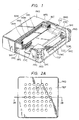
- Fug. 1 is a partially broken perspective view showing an overall magnetic bubble memory module of the present invention.
- Fig. 2A is a bottom view.
- Fig. 2B is a sectional view on line 2B - 2B of Fig. 2A.
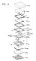
- Fig. 3 is an exploded perspective view showing a laminating structure.
- Fig. 4 is a view describing a substrate FPC.
- Fig. 5 is a plan view showing a substrate assembly BND where a chip DHI is loaded on the substrate FPC.
- Fig. 6 shows a view showing the chip CHI.
- Fig. 7 is a view describing lead bonding of the substrate assembly BND.
- Fig. 8 is a view describing a magnetic circuit PFC.
- Fig. 1 is a partially broken perspective view showing an overall magnetic bubble memory module of the present invention.
- Fig. 2A is a bottom view.
- Fig. 2B is a sectional view on line 2B - 2B of Fig.
- FIG. 9 is a view describing a producing method of the magnetic circuit PFC.
- Fig. 10 is a view showing an inner case RFSb.
- Fig. 11 is a view showing an outer case RFSa.
- Fig. 12 is an assembly drawing of the case RFS.
- Fig. 13 is a sectional view showing an assembly case RFS in which the substrate assembly BND and the magnetic circuit PFC are accomodated.
- Fig. 14 is a view describing the construction of a magnet BIM.
- Fig. 15 is a view describing a bias coil BIC.
- Fig. 16 is a sectional voew showing an assembly of the case RFS with which a pair of magnets BIM and the bias coil BIC are incorporated.
- FIG. 17 is a view showing an outer shield case SHIa.
- Fig. 18 is a view showing an inner shield case SHIb.
- Fig. 19 is an assembly drawing showing a shield case SHI.
- Fig. 20 is a sectional view showing the assembly shown in Fig. 16 incorporated in the shield case SHI.
- Fig. 21 is a view showing a packaging case PKG.
- Fig. 22 is a view describing the construction of a terminal-fixing plate TEF.
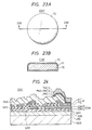
- Fig. 23 is a view showing the construction of a contact pad CNP.
- Fig. 24 is a sectional view showing the chip CHI.
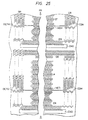
- Fig. 25 is a view showing the construction of a magnetic bubble detector D of the chip CHI.
- FIG. 33 shows the inner case RFS2b, where Fig. 33A is a plan view, and Fig. 33B is a sectional view taken on the line 33B - 33B of Fig. 33A.
- Fig. 34 shows the outer case RFS2a, where Fig. 34A is a plan view and Fig. 34B is a sectional view on the line 34B - 34B.
- Fig. 35 shows the status of only the outer and inner cases RFS2a and RFS2b assembled together.
- Fig. 36 shows the status of the chip CHI, the flexible substrate FPC2, and the magnetic circuit PFC accommodated in the outer case RFS2a.
- Fig. 37 shows the magnet body BIM2, where Fig. 37A is a plan vies, Fig.
- Fig. 37B is a side view and Fig. 37C is a sectional view taken on the line 37C - 37C.
- Fig. 38 shows the status of the magnet body BIM2 shown in Fig. 37 and the bias coil BIC shown in Fig. 15 accommodated in the case assembly RFS2 described with reference to Fig. 36, where Fig. 38A is a plan view and Fig. 38B is a sectional view taken on the line 38B - 38B.
- Fig. 39 shows the upper shield case SHI2a, where Fig. 39A is a plan view, Fig. 39B is the right side view and Fig. 39C is the bottom side view.
- Fig. 40 shows the lower shield case SHI2b, where Fig. 40A is a plan view, and Fig.
- FIG. 40B is a lower side view.
- Fig. 41 shows the magnetic shield cases SHI2a and SHI2b shown in Fig. 39 and Fig. 40 packaged therein with the intermediate assembly shown in Fig. 38, where Fig. 41A is a plan view and Fig. 41B is a sectional view taken on the line 41B - 41B.
- Fig. 42 shows a substrate for electrically connecting the shield case assembly shown in Fig. 41 to the pin grid external connection terminal, where Fig. 42A is a plan view, Fig. 42B is a sectional view taken on the line 42B - 42B, and Fig. 42C is a bottom view.
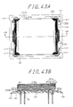
- Fig. 43 shows the status when the shield case assembly shown in Fig.
- Fig. 41 is packaged on the pin grid substrate TEF2 shown in Fig. 42, where Fig. 43A is a plan view and Fig. 43B is a sectional view taken on the line 43B - 43B.
- Fig. 44 shows an encapsulation cap, where Fig. 44A is a plan view, and Fig. 44B is a sectional view taken on the line 44B - 44B.
- Fig. 45 shows the finished structure of a series of modified embodiments described with reference to Fig. 32 thru Fig. 44, where Fig. 45A is a plan view, Fig. 45B is a sectional view taken on the line 45B - 45B and Fig. 45C is a right side view.
- Figs. 1 and 2A and 2B are views for describing one embodiment of a magnetic bubble memory module according to the present invention.
- Fig. 1 is a partially broken perspective view.
- Fig. 2A is a bottom view thereof.
- Fig. 2B is a sectional view on the line 2B - 2B of Fig. 2A.
- CHI denotes a magnetic bubble memory chip (hereinafter, referred as to a chip).
- CHI magnetic bubble memory chip
- FPC denotes a flexible aubstrate loaded on two chips CHI and having line group extensions for connecting between the chip CHI and an outer connection terminal at four corners (hereinafter, referred as to a substrate).
- COI denotes a driving coil surrounding two chips CHI in the almost same level therewith and disposed to make the opposite sides parallel with each other (hereinafter, referred as to a coil).
- COR denotes a picture frame core made of soft magnetic materials fixedly disposed so as to penetrate through a hollow portion of a square coil assembly COI (hereinafter, referred as to a core).
- This core COR and respective coils COI compose a magnetic circuit PFC for supplying an in-plane revolving magnetic field to the chip CHI.
- RFS denotes a case for confining a revolving magnetic field which serves to accomodate a central square part of the substrate FPC and the while two chips CHI and magnetic circuit PFC (hereinafter, referred as to a case).
- the case RFS is formed by working two dependent plates and the upper and the lower plates are electrically connected at the side sections of the case.
- RFS there is formed a drawn section around the case so as to narrow a gap of a central part in a somewhat wider range than the part on which the chip CHI is disposed. This drawn section can be utilized for positioning a magnet stated after.
- the case RFS has two effects, that is, functions of confinig a revolving magnetic field and mechanically supporting a weak substrate FPC.
- These inclined plates INN are formed to have the almost same gradient with that of the inclined plate INM and the inclined surfaces in the reverse directions to them.
- the inclined plate INM, the magnet plate MAG, the plate HOM for homogenizing a magnetic field and the inclined plate INN are disposed as piling them and integrated so as to compose a magnet body BIM for generating a bias magnetic field (hereinafter, referred as to a magnet body), when the magnet body composed of laminated plates is formed to uniformly have the overall thickness.
- a pair of magnet bodys BIM are attached on a central plane section surrounded by the drawn sections of the case RFS.
- bias coil BIC denotes a coil for generating a bias magnetic field disposed in a groove-like gap section between a peripheral portion of the magnet body BIM and the case RFS (hereinafter, referred as to a bias coil).
- the bias coil BIC is driven in case of arranging magnetism of the magnet plate MAG in accordance with the characteristics of the chip CHI or clearing all the bubbles of the chip CHI when there is accomplished the test as to fault of unnecessary-bubbles-generating.
- SHI denotes an outer magnetic shield case made of magnetic materials and for accomodating the case RFS in which the substrate loaded with said chip CHI and the magnetic circuit PFC are accomodated and, at the outside of the case, a pair of magnet bodys BIMa, BIMb and the bias coil BIC (hereinafter, referred as to a shield case).
- a shield case For the materials of the shield case SHI, it is preferable to employ the magnetic materials with high permeability ⁇ , large saturated flux density Bs and small retentiveness Hc.
- Permalloy or ferrite has such a characteristic, but the present embodiment selects iron-nickel alloy of Permalloy which is suitable for bending operation and can endure mechanical external force.
- Fig. 3. is a perspective view as to assembling for describing the order of pile-assembling respective components composing the above-stated magnetic bubble memory module.
- the substrate assembly BND assembled by loading two chips CHI on the substrate FPC having connecting sections for input and output wirings projected at 4 corners and a chip-loading section at the central portion is disposed in an outer case RFSa on which insulating sheets 36 are disposed by attaching.
- the substrate is filled with silicon resin STR (not shown). From the upper part, the inner case RFSb is engaged with the outer case RFSa and the side-contact portion between the outer case RFSa and the inner RFSb is electrically connected by means of soldering or the like.
- an upper magnet body BIMa and a lower magnet body BIMb are disposed on the concave drawn section provided on the outer surfaces of these outer case RFSa and inner case RFSb and then the bias coil BIC wound in order is desposed on the gap (not shown) formed by an outer edge section of this upper side magnet body BIMa and the inside of the inner case RFSb.
- These are accomodated in the outer shield case SHIa and further the inner shield case SHIb is incorporated therewith.
- the side-contact portion between the outer shield case SHIa and the inner shield case is electrically connected.
- the outer connection terminal-connecting sections of said substrate FPC projected at the four corners of the shield case SHI are bent to the rear surfaces of the inner shield case SHIa as shown in Fig. 4B and are incorporated so as to have a fixed form.
- a terminal-fixing plate TEF loaded with contact pads CNP at respective openings is disposed in contact with respective outer connection terminals covered by soldering or the like respectively provided at said terminal-connecting sections and respective outer connection terminals and the contact pads CNP are electrically connected with each other by means of soldering or the like.
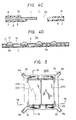
- Fig. 4 shows the substrate FPC.
- Fig. 4A is a plan view showing it.
- Fig. 4B is a plan view showing the connecting sections of the outer connection terminals projected at 4 corners, which are bent to the assembly.
- Fig. 4C is an enlarged sectional view taken on the line 4C - 4C in Fig. 4A.
- Fig. 4D is an enlarged sectional view taken on the line 4D- 4D in Fig. 4A.
- the substrate FPC includes a rectangular chip-loading section 1 at the central part, sections to be bent 2 (2a, 2b, 2c, 2d) whose widths are small at the four corners and rectangular outer connection terminal-connecting sections (hereinafter, referred as to a connecting section) 3 (3a, 3b, 3c, 3d), which are integrally formed so as to wholly have an almost windmill-like form.
- a connecting section 3a, 3b, 3c, 3d
- this chip-loading section 1 there are provided double-frame structure of square openings 4 (4a, 4b) to be loaded with the two chips CHI stated after and to be connected with the terminal sections thereof and three holes 5 (5a, 5b, 5c) for positioning and there is provided a projection 6 for positioning at the tip of the connecting section 3C.
- the patterns of lead wires 9a, circular outer terminals 9b, ellipsoidal coil lead-connecting terminals 9c, notes 9d, index marks 9e and the like as shown in Fig. 4A are formed by means of forming a copper thin film on a base film 7 made of a polyimide resin film with, for example, about 50 ⁇ m of thickness on which on epoxy system adhesive agent is coated as shown in Fig. 4C and then accomplishing etching of these films so as to form a required pattern. Further, a transparent or semi-transparent cover film 10 is attached and disposed on the upper surface of these films on which the adhesive agent 8 consisting of the same components with the above-stated agent is coated.
- an opening is formed on the base film 7 to be a chip CHI-loading side not shown in the drawings to tightly restricted dimensional tolerance. Then, an opening in relatively large dimensions is formed on an upper surface side cover film 10. Further, the lead wires 9a are exposed between the base film 7 and the cover film 10 and on the surface of these lead wires 9a, there is formed a tinning layer 11. Consequently, the opening form has a two-layered structure and at once a double-frame structure. On the other hand, in the connecting section 3, as shown in Fig.
- circular openings 12 are formed on the portions corresponding with said circular outer terminals 9b of the cover film 10 and elliptical outer terminals 9c not shown in the drawings and a soldering layer 13 by planting, dipping or the like is formed on the copper thin film patterns of the outer terminals 9b and 9c exposed from the opening 12.
- respective outer terminals 9b and 9c provided at these connecting sections 3 are connected to respective lead wires 9a continuously formed on the chip-loading section 1, respective connecting sections 3a, 3b, 3c, 3d and respective bending sections 2a, 2b, 2c, 2d.
- lead wires 9a are aggregated as respective blocks of respective connecting sections 3a, 3b, 3c, 3d at a part of respective opening edges of respective openings 4a, 4b and these tips of respective blocks are exposed in respective openings 4a, 4b.
- the lead wire 9a of the connecting section 3a is disposed at the left upper part of the opening 4a.
- the lead wire 9a of the connecting section 3b is disposed at the left lower part of the opening 4b.
- the lead wires 9a of the connecting section 3c are disposed at the right upper part of the opening 4a.
- the lead wires 9a of the connecting section 3d are disposed at the right lower part of the opening 4b.
- this substrate FPC is constructed so as to easily discriminate those patterns by looking through the cover film 10, because, in the step stated after, respective connecting sections 3a, 3b, 3c, 3d are combined for engagement, as shown in Fig. 4B by bending respective sections to be bent 2a, 2b, 2c, 2d and respective outer terminals 9b, 9c on which the soldering layer 13 is formed are exposed to the surface and further, the surfaces of the lead wires 9a, the note 9d and the index mark 9e are covered by the cover film 10.
- the substrate FPC employs a polyimide resin film and is constructed to have a windmill-like form providing respective connecting sections 3a, 3b, 3c, 3d through respective sections to be bent 2a, 2b, 2c, 2d at the four corners of the chip-loading section 1.
- the chip-loading section 1 and the connecting sections are made to have two-layered wiring structures.
- the area of the chip-loading section 1 is made larger and at once the outer terminal section can be made to have plural terminals. Accordingly, the overall form can be minimized.
- Fig. 5 is a plan view showing the construction wherein the chip CHI is loaded on the above-stated substrate FPC.
- two chips CHI are loaded on the chip-loading section 1 of the substrate FPC as disposing them between the openings 4a, 4b in parallel so as to complete the substrate assembly BND.
- One of the chips CHI is constructed by integrating two blocks of 1 Mbit as shown in an enlarged plan view of Fig. 6.
- two chips CHI have four blocks, that is, totally compose a 4 M bits chip.
- a large line shows a conductor pattern and a thin line shows a chevron pattern propagation path.
- a gold bump 15 is loaded by means of the lead-bonding using Au-Sn eutectic crystal caused by a pressure melding method as disposing a gold bump 15 between respective bonding pads 14 provided by gold-planting at the end of the chip CHI and the wiring leads 9a on which the tinning layer 11 is formed in the opening 4 of the substrate FPC as respectively shown in enlarged sectional views of Figs. 7A and 7B.
- the chip CHI it is possible to fixedly support the chip CHI by connecting the lead wires 9a in the openings 4a, 4b of the substrate FPC with the bonding pads 14 of the chip CHI by means of the lead-bonding using Au-Sn eutectic crystal. Accordingly, it is possible to greatly ameliorate strength for connection and thin the construction. Further, the surface of the chip CHI is covered by the chip-loading section 1 of the substrate FPC. Thus, the surface of the chip CHI is protected and at once it is possible to ameliorate handling efficiency and to hold mechanical strength of the substrate FPC.
- each chip CHI consists of two blocks and two chips CHI are composed of 4 blocks
- respective blocks can be distributively connected to respective connecting sections 3a, 3b, 3c, 3d which are the closes to respective blocks and thus the symmetric position of the chips CHI can be obtained so as to extremely facilitate a test, a check and the like.
- the substrate FPC provides four connecting sections 3a, 3b, 3c, 3d, it is possible to give and receive an input and an output signals having least noise by means of separating wirings for magnetic bubble detectors DET, map loops of each chip CHI and the like from the other wiring functions and aggregating them at one connecting section (refer to Fig. 6) and selectively disposing this connecting section at the location which is far away from a noise-generating source.
- Fig. 8 shows the magnetic circuit PFC.
- Fig. 8A is a perspective view.
- Fig. 8B is a plan view showing the driving magnetic circuit.
- a coil COI composed of four coils 20a, 20b, 20c and 20d by providing wirings (in the arrow direction are provided on the parallel sides facing to each other of the picture frame type of core COR made of soft magnetic materials and a X-coil 22a is composed by accomplishing series winding of the coils 20a and 20b on the sides facing to each other by way of a contact 21b and a Y-coil 22b is composed by accomplishing series winding of the coils 20c and 20b by way of a contact 21a.
- the magnetic circuit PFC constructed as stated above is completed by the step of, as shown in a perspective view of Fig. 9, providing windings in a rectangular parallelepiped-like magnetic core 23 made of one soft magnetic material and a tap 24 at each plural blocks, forming a pair of coils, for example, a pair of X-coils 22a composed of the coils 20a, 20b, by accomplishing series winding and providing a wider groove 25 and a less wide groove 26 respectively having fixed widths between respective coils 20a and 20b by means of cutting work, afterwards, engaging the wider grooves 25 divided into two parts at the center of this less wide groove 26 with each other rectangularly and attaching them so as to buildup a picture frame type of core as shown ia Fig. 8.
- the rectangular parallelepiped core 23 provides the coils 20a, 20b as providing the tap in the series direction, in case of completing the construction by assembling as shown in Fig. 8, there is no need to connect lines (contact) as crossing them with each other and thus it is possible to simplify winding.
- this magnetic circuit PFC is made to have a picture frame type of structure and thus is not disposed on the upper or the lower surface of the chip CHI. Thus, the thickness in the lamination direction is made smaller and thus the thinning of the circuit can be realized.
- Fig. 10 shows the inner case RFSb.
- Fig. 10A is a plan view.
- Fig. 10B is a sectional view taken on the line 10B - 10B of Fig. 10A.
- the inner case RFSb is built up of a frame type of drawn section 30 providing a concave portion at its center, bent sections 31 made by bending a pair of opposite side edges to each other upwardly about 90° and cut-away sections 32 made by cutting respective four corners in the slanting direction.
- This case RFSb is formed by press working of excellent conducting materials, for example, an oxygen free copper plate.
- the drawn section 30 and the bent sections 31 have a function of ameliorating mechanical strength of this inner case RFSb in the spiral direction and at once to suitably restrict outer length L in the vertical and transversial directions between each opposite bent sections 31 to each other.
- the drawn section 30 can suitably arrange the distance between the magnet body BIMb disposed at the outer surface sides of this case RFSb and the chip CHI disposed at the inner surface side thereof.
- the cut-away sections 32 provided at the four corners form the drawing section of respective sections 2a, 2b, 2c, 2d to be bent of the substrate FPC disposed in this case RFSb.
- oxygen free copper is employed but it is possible to employ copper, silver, or gold plate or the plate made by planting the alloy plate of these materials.
- Fig. 11 shows the outer case RFSa corresponding with the above-stated inner case RFSb.
- Fig. 11A is a plan view.
- Fig. 11B is a sectional view taken on the line 11B - 11B.
- this outer case RFSa is produced by using the same materials and manufacturing method with the above-stated inner case RFSb. It is comprised of a frame type of drawing section 33 providing a concave portion at its center, bent sections 34 made by bending two pairs of opposite side edges upwardly about 90° and cut-away sections 35 made by cutting away respective four corners in the slanting direction, similarly with the above-stated case.
- the outer case RFSa and the inner case RFSb as constructed above are assembled to be an integrated case RFS by means of inserting the inner case RFSb into the outer case RFSa and connecting them with each other to make the inner case RFSb be in contact with the outer surfaces of the bent sections 31 of the outer case RFSa, as shown in Fig. 12A which is the plan view of the case RFS and in Fig. 12B which is the sectional view taken on the line 12B - 12B of Fig. 12A.
- Fig. 13 is a sectional view showing the above-stated case RFS and the substrate assembly BND accomodated and disposed in said case.
- the outer case RFSa for example, about 0.1 mm of thickness of polyimid film 36 is disposeed and attached as an electrically insulating sheet.
- the substrate assembly BND and the magnetic circuit PFC are respectively disposed on this film 36 and the peripheral portion thereof.
- an epoxy system adhesive agent 37 is coated on the upper surface of the substrate assembly BND and then, in the upper part of them, the inner case RFSb is inserted, disposed and joined.
- the inner surfaces of the bent sections 34 of this outer case RFSa are mechanically and electrically jointed with the outer surfaces of the bent sections 31 of the inner case RFSb at the portions marked by X by means of metal flowing, soldering or the like.
- Silicon resin SIR fills in the gap between this outer case RFSa and this inner case RFSb so as to fixedly dispose the substrate assembly BND and the magnetic circuit PFC.
- the sections 2 (2a, 2b, 2c, 2d) to be bent of the substrate FPC are drawn from respective cut-away sections 32, 35 not shown provided at the four corners of these outer case RFSa and inner case RFSb to the outside.
- 38 denotes a lead wire for connecting coils COI with each other or connecting the coil COI with an external terminal 9c provided on the substrate FPC.
- induced current is flown through the case RFS so as to form a closed loop.
- This induced current serves to confine a revolving magnetic field in the case RFS and thus the uniform revolving magnetic field is supplied to the chip CHI.
- the chip CHI loaded on the substrate FPC and the magnetic circuit PFC are respectively disposed so as to be caught in the central concave portion and in the peripheral convex portion between the outer case RFSa and the inner case RFSb.
- the volume covered by the outer case RFSa and the inner case RFSb is diminished, a VI product ( ⁇ volume) can be reduced and thus it is possible to miniaturize the magnetic circuit PFC for generating a revolving magnetic circuit.
- Fig. 14 shows the magnet body BIM.
- Fig. 14A is a plan view thereof.
- Fig. 14B is a side view thereof.
- Fig. 14C is an elevational view thereof.
- the magnet body BIM is formed by piling up an inclined plate INN made of non-magnetic materials such as copper and having one predetermined inclined surface of the opposite surfaces, a plate HOM for homogenizing a magnetic field whose thickness is uniform and to be disposed at the inclined surface side of this inclined plate INN, a magnet plate MAG whose thickness is uniform and to be disposed at the upper surface side of this plate for homogenizing a magnetic field HOM and an inclined plate INM havong an inclined surface and to be disposed at the upper surface side of this magnet body MAG and then integrating them by means of an epoxy system adhesive agent.
- an inclined plate INM havong an inclined surface and to be disposed at the upper surface side of this magnet body MAG and then integrating them by means of an epoxy system adhesive agent.
- the bias coil is formed by thermal-depositing thermosetting resin coated on the outer surfaces of respective windings 40 and loading respective windings 40 and loading respective windings 40 by pressure-welding. Then, by cooling it, respective windings 40 are hardened in the united state of windings and thus having a predetermined picture frame.
- Fig. 16 is a sectional view showing the case RFS desoribed in Fig. 13, the above-stated magnet body BIM and bias coil BIC incorporated in the case.
- an upper magnet body BIMa and a lower magnet body BINb are respectively disposed and jointed on the upper and the lower surfaces of the case RFS assembly accomodated in the substrate assembly BND and the magnetic circuit PFC.
- the bias coil BIC is accomodated and disposed in a picture frame groove section formed by being surrounded by the peripheral portion of this upper magnet body BIMa and the bent sections of the inner case RFSb.
- the upper magnet body BIMa and the lower magnet body BIMb are formed by means of the same materials and in the same dimensions with each other.
- magnet bodys BIMa and BIMb at their inclined plate INN sides are respectively disposed closely in a concave portion surrounded by the drawn section 30 of the inner case RFSb and a concave portion surrounded by the drawn section 33 of the outer case RFSa.
- Fig. 18 shows an inner shield case SHIb corresponding with the above-stated outer shield case SHIa.
- Fig. 18A is a plan view thereof.
- Fig. 18B is a sectional view taken on the line 18B - 18B of Fig. 18A.
- this inner shield case SHIb is formed by the same materials and manufacturing method with the outer shield case SHIa stated above. It is comprised of, similarly with the above, a flat section 55, sections 56 made by bending two pairs of opposite side ends upwardly about 90°, concave portions 57 made by cutting away part of the central parts of these bent sections 56 and cut-away sections 58 made by cutting respective corners or these bent sections.
- each opposite bent sections 56 have the almost same outside length betweeen them with the inside length L4 between each opposite bent sections 52 of the above-stated outer shield case SHIa and the height H of the inner shield case SHIb is lower than that of the outer shield case SHIa.
- Fig. 19A is a plan view showing the outer shield case SHIa and the inner shield case SHIb constructed above.
- Fig. 19B is a sectional view taken on the line 19B - 19B.
- the shield case SHI is integrally built up by means of inserting the inner shield case SHIb in the outer shield case SHIa and accomplishing spot-welding or solder-welding in relation to the concave portion 59 formed by the concave portion 53 of the outer shield case SHIa and the concave portion 57 of the inner shield case SHIa so as to magnetically and mechanically fix both shield cases with each other.
- Fig. 20 is a sectional view showing the above-stated shield case SHI assembly, the case RFS assembly incorporating the substrate assembly BND and the magnetic circuit PFC therein as described in Fig. 16 and the assembly consisting of a pair of magnet body BIMa and BIMb and the bias coil BIC respectively incorporated in said shield case SHI assembly.
- the upper magnet body BIMa at the bottom to the center, the bias coil BIC at the peripheral portion, the case RFS assembly (incorporating the substrate assembly BND, the magnetic circuit PFC and the like therein) the lower magnet body BIMb are sequentially laminated and disposed and then the inner shield case SHIb is inserted to the outer shield case.
- this resin plate 60 there is formed along the peripheral portion a groove 65 which has the almost same depth with the depth of said openings, different width in the horizontal direction therefrom and a concave state in section.
- the inside of this groove 65 serves as the passage section and the connection section of the coil COI windings and the bias coil BIC windings stated above,
- the corner portions of this resin plate 60 are not formed as concave forms. They have a predetermined plate thickness and serve as contact surfaces to the inner side surfaces of the above-stated packaging case PKG.
- the rear side of the resin plate 60 is formed to have a two-stepped structure which, namely, has two thicknesses.
- Fig. 23 shows a contact pad CNP.
- Fig. 23A is a plan view thereof.
- Fig. 23B is a sectional view thereof.
- the contact pad CNP is formed by means of accomplishing pressing work of good conducting materials, for example, a copper plate whose thickness is about 0.5 mm to punch out a piece member 70 and then forming a nickel-planting layer 71 and a gold-planting layer 72 on the surface of the piece member 70.
- the shield case assembly described in Fig. 20 is inserted to the packaging case PKG stated above.
- respective connecting sections 3a, 3b, 3c, 3d of said substrate assembly BND (refer to Fig. 4A) are projected from the four corners of this packaging case PKG as bent at about 90 degrees on the basis of respective sections to be bent 2a, 2b, 2c, 2d.
- respective components are fixedly disposed in this packaging case PKG by accomplishing a resin-molding to the four corners of this packaging case PKG by means of a potting method.
- these connecting sections 3a 3b, 3c, 3d are respectively bent about 90 degrees by the corresponding sections to be bent 2a, 2b, 2c, 2b, and then are engaged on the outer surface of the inner shield case SHIb shrough an adhesive agent as shown in Fig. 4B. Then, the contact pads CNP are loaded in respective openings provided on the rear side of said terminal-fixing plate TEF or the sides of the contact pad CNP are made solid by means of an adhesive agent and then the treated contact pads CNP are inserted in the packaging case PKG so as to be disposed in contact with respective connecting sections 3a, 3b, 3c, 3d.
- respective external terminals 9b provided on respective connecting sections 3a, 3b, 3c, 3d corresponds with the arrangement pitch for respective contact pads CNP.
- respective external terminals 9b are electrically in contact with the contact pads CNP.
- a heated thing whose tip is slender or something like that is inserted to each through holes 61 from the rear side of the disposed terminal-fixing plate TEF so as to attach the contact pads CNP with the external terminals by pressure welding. Consequently, respective external terminals 9b are electricaly connected with the corresponding contact pads CNP and at once the terminal-fixing plate TEF is mechanically fixed to the contact pads so as to complete the magnetic bubble memory module as shown in Fig. 2.
- SP1 denotes a first spacer which serves to form, for example, SiO2 whose thickness is 3000 ⁇ by means of a gaseous phase chemical reaction.
- CON 1 and CON 2 denote two conducting layers and has a function of controlling generation of bubbles, duplication (division) thereof and exchanging thereof as stated above.
- a lower first conducting layer CON 1 and an upper second conducting layer CON 2 are respectively made of materials such as Mo and those such as Au.
- SP2 and SP3 respectively denote layer-insulating films (a second and a third spacers) made of polyimide resin or the like for performing electrical insulation between the conducting layers CON and a transfer pattern layer P made of Permalloy or the like formed thereon.
- P denotes the layer utilized as a transfer path of bubbles, a dividing, a generating, an exchanging and a seraching sections of bubbles and a guardrail section. In the description stated after, it is described as a transfer pattern layer for convenience' sake.
- Fig. 25 shows a D section of a bubble detector.
- MEM denotes a main magnetic resistance element for detecting the existence of bubbles by means of variation of a resistance value provided in case of passing the bubbles extended like a band in the lateral direction through the element.
- MED denotes a dummy magnetic resistance element having the same pattern form with those of the main magnetic resistance element and is utilized for detecting noise components brought about by the influence of a revolving magnetic field and the like.
- MEM main magnetic resistance element
- PR denotes the transfer direction of bubbles.
- ER denotes a bubble eraser and serves to erase bubbles when they attain to the conducting layer CND.
- the guardrail GR consisting of pattern blocks lining up in three files is provided around this detector D and between the dummy and the main detections and serves to get the unnecessary bubbles generated in the inside of the guardrail GR out of the guardrail and to prevent entering the unnecessary bubbles generated in the outside of the guardrail GR into the inside thereof.
- the patterns except the conducting layer CND pattern show the transfer pattern layer P described in Fig. 24.
- a signal-to-noise ratio (S/N ratio) is ameliorated by means of forming the magnetic resistance elements MEM and MED by a multilayered magnetic layer.
- the efficiency of the guardrail GR can be improved because of heightening a discharging factor for unnecessary bubbles by means of reducing retentiveness Hc.
- Fig. 26 shows a magnetic bubble-generator GEN.
- the current generated in the magnetic bubbles can be made smaller by making the transfer pattern layer P multilayered and thus it is made possible to lengthen the life of the conducting layer CND of the magnetic bubble-generator. Accordingly, the driving circuit for the conducting layer CND can employ a semiconductor element with a small current capacity value and thus its cost can be made lower.
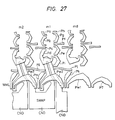
- Fig. 27 shows a minor loop m composed of transfer patterns such as Pa - Ph and the like, a write major line WML composed of the transfer patterns such as Pw1 to Pw3 and the like and a swap gate section composed of a hairpin conducting layer CND.
- P7 is the same with the transfer pattern P7 in the bubble-generator GEN shown in Fig. 26.
- the bubbles generated in the bubble-generator GEN are transferred to the write major line WML through the P1 to P7 transfer pathes.
- the magnetic bubbles in the transfer pattern Pd of the minor loops ml are transferred through the transfer patterns P l and Pm to the transfer pattern Pw3 of the major line WML and the magnetic bubbles from the major line PW1 are transferred through the transfer patterns Pk, Pj and Pi to the transfer pattern Pe of the minor loop in order to accomplish an exchange of bubbles, that is, informations with each other.
- the swap gate is not provided in the minor loop md at the right end, because it is a dummy loop where magnetic bubbles are not injected for reducing a peripheral effect. As described above, it is possible to accomplish an exchange of magnetic bubbles with a small current value by means of making the transfer pattern layers Pi to Pm at the exchange location multilayered.
- the magnetic bubbles are usually transferred on the route of Pn to Pg and Ps to Px.
- the conducting layer CND is energized, the bubbles is divided at the location of the transfer pattern Pg and one divided magnetic bubble is transferred to a read major line RML by way of Py and P8 to P10.
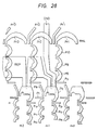
- the magnet body MAG is disposed as about 2 degrees tilted in relation to the chip CHI. This is designed to apply a bias magnetic field Hb to the chip CHI in the direction a little shifted from the vertical. Thus, it is possible to generate a holding magnetic field Hdc for ameliorating a atart and a stop margins of the bubble transfer to raise about 6(Oe)(Fig. 29A).
- the series magnetic field Hz is made to have a component Hdc on the xy plane.
- the direction of this in-plane component Hdc is slanted to coincide with the start and stop (St/Sp) direction in the revolving magnetic field Hr(+ x-axis direction).
- This component Hdc on this xy plane is a well-known magnetic field effectively served as the start and stop (St/Sp) operation of the revolving magnetic field Hr and called as a holding field. Further, magnitude of the bias magnetic field Hb vertically functioned on the chip CHI plane is made to be Hz ⁇ cos ⁇ .
- Hr denotes a revolving magnetic field applied from the external.
- Hr' denotes a revolving magnetic field functioning to the chip CHI.
- the revolving magnetic field Hr' functioning to the chip CHI is made to be a synthesis of the revolving magnetic field Hr applied from the external and the in-plane component Hdc and the center O' of the revolving magnetic field Hr' is shifted in parallel by the in-plane component Hdc in the start and stop (St/Sp) direction, that is, + x-axis direction.
- the intensity of the revolving magnetic field Hr applied from the external is
- of the revolving magnetic field effectively functioning to the chip CHI is variable in accordance with the phase of the revolving magnetic field Hr.
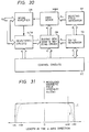
- RF denotes a circuit for generating a revolving magnetic field Hr by flowing the current whose phase difference is 90 degrees through the X- and Y-coils of the chip CHI.
- SA denotes a sense amplifier for sampling a minute bubble-detecting signal from the magnetic resistance element of the chip CHI in accordance with a timing of the revolving magnetic field, sensing and amplifying it.
- DR denotes a driving circuit for generating the bubbles in relation to the write in the magnetic bubble memory device MBM, flowing current through respective replicate functioning conductors in relation to swapping and reading in accordance with a predstermined timing and driving a bias coil BIC.
- the above-stated circuits are synchronized by means of a timing-generator TG so as to be operated in synchronization with a cycle and a phase angle of the revolving magnetic field Hr.
- the substrate FPC2 has a copper foundation lead wire pattern which is formed by means of patterning with etching technique the copper film which is lined with epoxy system adhesive onto the base film composed of a polyimide resin film having the thickness of approsimately 50 ⁇ m.
- a Ni-plating layer and an Au-plating layer are formed successively by the electroplating method, etc.
- This Au-plating layer is provided for the purpose of preventing from the electrical migration of the copper layer or making the thermocompression bonding of the magnetic bubble memory chip CHI with the bonding pad easy.
- the Ni layer is used for the purpose of improving adherence between the copper layer and the Au-layer.
- the lead wire pattern 100 of each frame is connected at this stage by the frame-shaped pattern provided along the periphery shown in the drawing and the estended portion 100e, but it is for electroplating.
- the external connection parts 100c of lead wire 100 are concentrated in two directions as previously described.
- One of the reasons for the concentration in the left and right directions instead of upward and downward directions is to obtain compatibility with the 35mm film described above.
- Another reason is as follows.
- the memory chip CHI is face-up bonded underneath the film substrate FPC2, but the substrate FPC2 and the chip CHI are inclined in left and right directions in the drawing as described later. (Under the same bias condition as Fig. 2B, inclination toward the right is arranged such that the left side is high and the right side is low with the magnet body as the reference.)
- the substrate FPC2 is not inclined in upward and downward directions.
- Fig. 33 shows the inner case RFS2b.
- Fig. 33A is a plan view
- Fig. 33B is a sectional view taken on the line 33B - 33B of Fig. 33A.
- This case RFS2b is different from that shown in Fig. 10 in such points that the drawing section is omitted and the bottom plate thickness gets thicker as getting closer to the righthand side.
- the lower surface of the bottom plate is tapered lowering toward the right at an angle of 1.7 degree against the upper surface.
- a plate HOM for homogenizing a magnetic field and the magnetic body of a permanent magnet are provided on the upper surface and the chip CHI is arranged on the lower surface.
- the inclination of thickness is provided for the purpose of giving to the chip CHI a holding magnetic field Hdc due to the inclination between the magnetic body and the chip CHI.
- the inclined surface of the conductor case described above is formed by means of press work with about 300 tons (inclined padding process). As other forming method, such inclined surface may be formed either by cutting or by tilting a roller during rolling process.
- Fig. 35 shows the status of only the outer and inner cases RFS2a and RFS2b assembled together (The chip CHI, the film substrate FPC2 and the magnetic core PFC are omitted in the drawing in the same way as Fig. 12).
- Fig. 12A is a plan view and Fig. 12B is a sectional view taken on the line 35B - 35B.
- Fig. 36 shows the status of the chip CHI, the flexible substrate FPC2, and the magnetic circuit PFC accommodated in the outer case RFS2a (the status before covering up with the inner case RFS2b).
- Fig. 36A is a plan view and Fig. 36B is a sectional view taken on the line 36B - 36B.
- the chip CHI is mounted on the substrate before being accommodated in the case RFS2a.
- the chip CHI is mounted on the back of the flexible substrate FPC2 keeping the main surface up (face up), on which bonding pads, lead wires and the transport path are located. It is needless to say that connection is made at the lead wire part 100a of the substrate FPC2 and the pad area of the chip CHI, but both are bonded by means of thermocompression of the lead wire part 100a on the pad with toolings such as a capillary.
- the film substrate 101 consisting of plurality of substrates FPC2 is separated into individual substrate FPC2, and unnecessary lead wire parts and reinforced area which were used in plating the periphery are cut off as shown in Fig. 36A.
- the conductor case RFS2a is applied with adhesives such as epoxy system resin by a stamping method, where the back of the chip CHI which was bonded on the film substrate FPC2 is adhered.
- the relation at this time between the locations of the chip CHI and the case RFS2a can be determined precisely by means of the cut-away section 135 of the case RFS2a and external connecting sections 102a thru 102d. If necessary, more fine positioning adjustment is feasible by using jigs, etc.
- the magnetic circuit PFC is housed in the groove formed by the drawing section 133 of the case RFS2a and the outside wall 134.
- potting with silicone resin REG2 is performed around the chip CHI.
- the selicon resin REG2 increases its fluidity by heating treatment and gets into between the back of the flexible substrate FPC2 and the main surface of the chip CHI by means of the capillary action, thereby protecting the chip CHI against adhesion of dust and permeation of moisture.
- Fig. 37 shows the magnet body BIM2.
- Fig. 37A is a plan vies
- Fig. 37B is a side view
- Fig. 37C is a sectional view taken on the line 37C - 37C.
- the magnet body BIM 2 shown differs from that (BIM) shown in Fig. 14 in such a point that inclined plates INM and INN are omitted.
- Fig. 38 shows the status of the magnet body BIM2 shown in Fig. 37 and the bias coil BIC shown in Fig. 15 accommodated in the case assembly RFS2 described with reference to Fig. 36.
- Fig. 38A is a plan view and Fig. 38B is a sectional view taken on the line 38B - 38B.
- the upper magnet body BIM2a and the bias coil BIC are mounted on the plate-shape inner case RFS2b, and the lower magnet body BIM2b is mounted on a flat part surrounded by the drawing section 38 of the outer case RFS2a.
- Fig. 38 shows the status of the magnet body BIM2 shown in Fig. 37 and the bias coil BIC shown in Fig. 15 accommodated in the case assembly RFS2 described with reference to Fig. 36.
- Fig. 38A is a plan view and Fig. 38B is a sectional view taken on the line 38B - 38B.
- the upper magnet body BIM2a and the bias coil BIC are mounted on the plate-shape inner case RFS2b, and the lower magnet body BIM2b is mounted on a flat part surrounded by the drawing section 38 of the outer case RFS2a.
- the chip CHI and the magnetic circuit PFC are inclined in left and right directions with reference to a parallel surface formed by upper and lower magnet bodies BIM2a and BIM2b.
- the condition for arranging the magnetic circuit PFC and the chip CHI in parallel remains unchanged from those embodiments shown in Fig. 13 and Fig. 16, but the thickness of the chip CHI, the thickness of the magnetic circuit PFC and the height of the drawing section 38 of the outer case RFS2a are designed so that the uppermost end surface of the magnetic circuit PFC and the upper surface of the chip CHI are almost even with each other, thereby preventing from application of the stress to the flexible substrate FPC2.
- Fig. 39 shows the upper shield case SHI2a.
- Fig. 39A is a plan view
- Fig. 39B is the right side view
- Fig. 39C is the bottom side view.
- the plane figure of the upper shield case SHI2a is square in shape and is symmetrical for any axis of four center lines passing the same point (not shown), horizontal, vertical, and going up and down at 45° toward the right.
- the cut-away sections 154 at four cormers making a right angle with the 45° center lines are provided for the purpose of having lead wire portions 102a thru 102d pass through at the four corners of the film substrate FPC shown in Fig. 32.
- 151 denotes the plane section of the case
- 152 denotes the upright wall section.
- Protruded sections 152a thru 152d are provided at the center part of each side of the walls 152.
- the height of protruded sections 152a and 152c on left and right sides is to be h2, and the height of protrusion itself (h2 - h1) is to be the same as the thickness t0 of the lower shield case SHI2b shown in Fig. 40.
- the height of the protruded sections 152b and 152d on upper and lower sides is to be h3, and the height of protrusion itself (h3 - h1) is to be slightly bigger than the thickness t0 of the lower shield case SHI2b.
- Fig. 40 shows the lower shield case SHI2b.
- Fig. 40A is a plan view
- Fig. 40B is a lower side view.
- Fig. 41 shows the magnetic shield cases SHI2a and SHI2b shown in Fig. 39 and Fig. 40 packaged therein with the intermediate assembly shown in Fig. 38.
- Fig. 41A is a plan view and Fig. 41B is a sectional view taken on the line 41B - 41B.
- the assembly shown in Fig. 41 still includes terminals 109a, 109b, and extended portion of lead wires for plating that are not required for the final assembly, however, it is possible to perform the operation test and selection of acceptable products for the intermediate assembly at this stage, thereby reducing the average assembly cost per device.
- the upper and lower shield cases RFS2a and RFS2b are welded together by the spot welding method or the laser welding method.
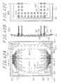
- Fig. 42 shows a substrate for electrically connecting the shield case assembly shown in Fig. 41 to the pin grid external connection terminal.
- Fig. 42A is a plan view
- Fig. 42B is a sectional view taken on the line 42B - 42B
- Fig. 42C is a bottom view.
- the ceramic substrate 201 provided with lead wires 205 thereon includes the upper thruhole connection terminals 206, the thruholes 207 and the lower thruhole connection terminals 208.
- the other end 205a of the lead wires 205 shows the portion where the outer lead portion 100c of the flexible substrate FPC2 is connected.
- the external connection pins 204 arranged in grid shape are connected electrically with the upper terminals 206 through conductive layers formed in the thruholes 207.
- the lead wires 205 those that are a little thicker than others are for connecting X coil, Y coil and bias coil (2 terminals each of Ix,Iy and Ib).
- 203 denotes a frame-shaped sealing ring, which is adhered to the edge of the ceramic substrate 201 by silver brazing alloy material, etc., and it is arranged such that the packaging cap PKG2 described later is welded to the portion protruding outside from the substrate 201.
- double metalized layers are formed on the portion of the ceramic substrate 201 where lead wires 205, terminals 206, 208, thruholes 207 and frames 203 are brazed.
- the grid pins 204 and the frame 203 are brazed to the ceramic substrate 201 with silver brazing alloy material.
- the double metalized layers have such function as to increase the adhesive strength.
- Ni and Au layers are electroplated successively on the pin grid substrate TEF2, i.e., on the exposed double metalized layers and KOVAR material.
- the Ni layer is provided for the purpose of increasing the adhesive strength between the doubled layer and the Au layer.
- Fig. 44 shows an encapsulation cap.
- Fig. 44A is a plan view
- Fig. 44B is a sectional view taken on the line 44B - 44B.
- the bottom part 223 is welded to a portion exposed from the ceramic substrate 201 of the frame 203 made of KOVAR by the resistance welding method, etc. Accordingly, the step difference between the exposed portion of the frame 203 and the side of the ceramic substrate 201 is useful for positioning in fitting the cap PKG2.
- Fig. 45 shows the finished structure of a series of modified embodiments described with reference to Fig. 32 thru Fig. 44, that is, the structure of the intermediate assembly shown in Fig. 43 encapsulated with the cap PKG2 shown in Fig. 44.
- Fig. 45A is a plan view
- Fig. 45B is a sectional view taken on the line 45B - 45B
- Fig. 45C is a right side view.
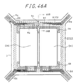
- Fig. 46 shows a further modification in which bias coil BIC is formed on the flexible printed circuits substrate FPC, where Fig. 46A shows a plane view of a major area of the flexible substrate FPC3 and Fig. 46B shows the intersection view of 46B-46B line inFig. 46A.
- Fig. 46 same parts as that of Fig. 4 are designated by same reference.
- bias coil BIC2 is patterned and printed on the flexible substrate FPC3 around the chip CHI which is mounted on the flexible substrate FPC3.
- a printed coil winding 9f has two terminal parts electrically led and extended in the direction of outer leading portion 2a of the flexible substrate FPC2 by the interconnection pattern 9g and electrically connected with terminals 9c for connecting coil leads shown in Fig. 4A.
- thin cuprum film is formed on a first base film 7 of about 50 ⁇ m thickness polyimide through an adhesive agent 8 and is etched in a predetermined pattern to form coil interconnecting lead patterns 9h and 9g as well as interconnecting pattern 9a.
- a second base film 7a is further formed by an adhesive agent.
- Cu thin film is further bonded with the aid of the adhesive agent 8 on the base film 7a and is etched in a loop-like pattern to form coil winding 9f.
- the inner terminal portion of the coil winding 9f is led outer the winding by way of the first-level interconnection pattern 9h which is electrically connected with the second level coil winding pattern 9f at the through-hole perforated in the second base film 7a.
- the dotted lines shows the second-level conductive pattern, and small circular mark designates the through-holes formed in the base film 7a.
- the third polyimide film 10 shown in Fig. 46B is further bonded on the printed film by an adhesive agent 8 to cover the entire surface.
- bias coil BIC2 is formed with the flexible printed circuits substrate, the number of components as well as accomodating steps is reduced to achive low cost manufacturing as well as high reliability.
Landscapes
- Coils Or Transformers For Communication (AREA)
- Measuring Magnetic Variables (AREA)
Claims (5)
- Module de mémoire à bulles magnétiques (Fig. 43B), comprenant:
une puce (CHI, Fig. 36B) de mémoire à bulles magnétiques pour stocker des informations;
un moyen d'accès (PFC sur la Fig. 36B ou RF sur la Fig. 30) pour appliquer un champ magnétique rotatif (Hr) à ladite puce;
une pellicule souple d'interconnexion (FPC2) ayant une pluralité de câblages reliés électriquement à ladite puce, et une pluralité de bornes extérieures (100c) disposées sur les côtés gauche et droit et reliées électriquement à ladite puce par l'intermédiaire desdits câblages;
caractérisé par
un substrat d'interconnexion (201) ayant un premier et un second groupes de bornes de connexion disposées sur les côtés gauche et droit et reliées électriquement respectivement auxdites bornes extérieures gauches et droites (100c) de ladite pellicule, une pluralité de bornes extérieures (206) disposées entre lesdits premier et second groupes de bornes de connexion et une pluralité de conducteurs d'interconnexion reliant électriquement lesdits groupes de bornes de connexion auxdites bornes extérieures. - Module selon la revendication 1, caractérisé en ce que
une pluralité de broches (204) sont fixées perpendiculairement à la surface inférieure dudit substrat et sont reliées électriquement auxdites bornes extérieures (206). - Module selon la revendication 2, caractérisé par
une couronne (203), qui est formée sur ladite surface inférieure au niveau de la partie formant le bord dudit substrat et qui dépasse du bord dudit substrat; et
un capot (PKG2), qui est fixé à la partie saillante de ladite couronne et qui couvre la surface supérieure dudit substrat. - Module selon l'une quelconque des revendications précédentes,
caractérisé par
un boîtier conducteur rectangulaire (RFS2) pour confiner le champ rotatif à l'intérieur et contenant ladite puce, ledit boîtier ayant des ouvertures aux angles supérieur gauche, inférieur gauche, supérieur droit et inférieur droit (132, 135) de celui-ci; et
dans lequel ladite pellicule souple d'interconnexion (FPC2) a une pluralité de bornes intérieures (100a) reliées électriquement à ladite puce, des parties prolongatrices (102a à 102d) avec des câblages conducteurs s'étendant à l'extérieur dudit boîtier au niveau desdits quatre angles, et est respectivement reliée auxdites bornes extérieures (100c).
lesdits conducteurs présents auxdits angles supérieur gauche et inférieur gauche s'étendant en outre respectivement vers le bas et vers le haut pour être reliés électriquement aux bornes extérieures du côté gauche, et lesdits conducteurs présents auxdits angles supérieur droit et inférieur droit s'étendant en outre respectivement vers le bas et vers le haut pour être reliés électriquement aux bornes extérieures du côté droit. - Module selon la revendication 4, caractérisé en ce que
ledit moyen d'accès (PFC sur la Fig. 36B ou RF sur la Fig. 30) comprend une bobine (COI), ladite bobine se prolongeant à l'extérieur dudit boîtier au niveau de ladite ouverture (cf. Fig. 36A, repères Ix, Iy).
Applications Claiming Priority (6)
| Application Number | Priority Date | Filing Date | Title |
|---|---|---|---|
| JP8859385 | 1985-04-26 | ||
| JP88593/85 | 1985-04-26 | ||
| JP88672/85 | 1985-04-26 | ||
| JP60088672A JPS61248292A (ja) | 1985-04-26 | 1985-04-26 | 磁気バブルメモリ装置 |
| JP60090824A JPH0646510B2 (ja) | 1985-04-30 | 1985-04-30 | 磁気バブルメモリ |
| JP90824/85 | 1985-04-30 |
Publications (3)
| Publication Number | Publication Date |
|---|---|
| EP0201781A2 EP0201781A2 (fr) | 1986-11-20 |
| EP0201781A3 EP0201781A3 (en) | 1989-03-15 |
| EP0201781B1 true EP0201781B1 (fr) | 1991-11-27 |
Family
ID=27305854
Family Applications (1)
| Application Number | Title | Priority Date | Filing Date |
|---|---|---|---|
| EP86105731A Expired - Lifetime EP0201781B1 (fr) | 1985-04-26 | 1986-04-25 | Module de mémoire à bulles magnétiques |
Country Status (3)
| Country | Link |
|---|---|
| US (2) | US4975871A (fr) |
| EP (1) | EP0201781B1 (fr) |
| DE (1) | DE3682615D1 (fr) |
Families Citing this family (4)
| Publication number | Priority date | Publication date | Assignee | Title |
|---|---|---|---|---|
| US5936850A (en) * | 1995-03-03 | 1999-08-10 | Canon Kabushiki Kaisha | Circuit board connection structure and method, and liquid crystal device including the connection structure |
| US7200033B2 (en) * | 2004-11-30 | 2007-04-03 | Altis Semiconductor | MRAM with coil for creating offset field |
| US20080296806A1 (en) * | 2007-05-31 | 2008-12-04 | Husky Injection Molding Systems Ltd. | Hot Runner Melt Pre-Compression |
| US20080296805A1 (en) * | 2007-05-31 | 2008-12-04 | Husky Injection Molding Systems Ltd. | Hot Runner Melt Pre-Compression |
Citations (1)
| Publication number | Priority date | Publication date | Assignee | Title |
|---|---|---|---|---|
| JPS59185087A (ja) * | 1983-04-04 | 1984-10-20 | Hitachi Ltd | 磁気バブルメモリ装置 |
Family Cites Families (12)
| Publication number | Priority date | Publication date | Assignee | Title |
|---|---|---|---|---|
| NL7204639A (fr) * | 1972-04-07 | 1973-10-09 | ||
| US3864671A (en) * | 1972-04-10 | 1975-02-04 | Hughes Aircraft Co | Package structure for movable magnetic domain devices |
| JPS5545987B2 (fr) * | 1974-10-02 | 1980-11-20 | ||
| US4178636A (en) * | 1976-02-20 | 1979-12-11 | International Business Machines Corporation | Gradientless propulsion of magnetic bubble domains |
| JPS5316534A (en) * | 1976-07-30 | 1978-02-15 | Hitachi Ltd | Test unit for magnetic bubble wafer |
| US4165535A (en) | 1977-09-30 | 1979-08-21 | International Business Machines Corporation | Bubble memory drive system using a picture frame core and a reflection box |
| US4180863A (en) * | 1978-06-30 | 1979-12-25 | International Business Machines Corporation | Magnetic domain device modular assembly |
| US4377854A (en) * | 1979-06-25 | 1983-03-22 | International Business Machines Corporation | Substrate for magnetic domain device |
| JPS6015341A (ja) | 1983-07-07 | 1985-01-26 | Koyo Jidoki | 複数ロ−ルの連続供給装置 |
| JPS6015888A (ja) * | 1983-07-06 | 1985-01-26 | Hitachi Ltd | 磁気バブルメモリモジユ−ル |
| JPS6016540A (ja) | 1983-07-07 | 1985-01-28 | Meiji Seika Kaisha Ltd | 乾葡萄の処理方法 |
| JPS6066456A (ja) | 1983-09-22 | 1985-04-16 | Matsushita Electric Ind Co Ltd | 集積回路パッケ−ジの製造方法 |
-
1986
- 1986-04-25 EP EP86105731A patent/EP0201781B1/fr not_active Expired - Lifetime
- 1986-04-25 DE DE8686105731T patent/DE3682615D1/de not_active Expired - Lifetime
-
1988
- 1988-07-07 US US07/216,184 patent/US4975871A/en not_active Expired - Fee Related
-
1989
- 1989-11-06 US US07/432,327 patent/US4972369A/en not_active Expired - Fee Related
Patent Citations (2)
| Publication number | Priority date | Publication date | Assignee | Title |
|---|---|---|---|---|
| JPS59185087A (ja) * | 1983-04-04 | 1984-10-20 | Hitachi Ltd | 磁気バブルメモリ装置 |
| US4663737A (en) * | 1983-04-04 | 1987-05-05 | Hitachi, Ltd. | Magnetic bubble memory unit |
Also Published As
| Publication number | Publication date |
|---|---|
| EP0201781A3 (en) | 1989-03-15 |
| DE3682615D1 (de) | 1992-01-09 |
| EP0201781A2 (fr) | 1986-11-20 |
| US4975871A (en) | 1990-12-04 |
| US4972369A (en) | 1990-11-20 |
Similar Documents
| Publication | Publication Date | Title |
|---|---|---|
| US3864671A (en) | Package structure for movable magnetic domain devices | |
| US4972369A (en) | Magnetic bubble memory module with interconnection member | |
| EP0190642B1 (fr) | Module de mémoire à bulles magnétiques | |
| EP0200173B1 (fr) | Module de mémoire à bulles magnétiques | |
| EP0201007A2 (fr) | Méthode pour mesurer le champ de maintien d'un module de mémoire à bulles magnétiques utilisant un noyau en forme de cadre d'image | |
| EP0201009A2 (fr) | Module de mémoire à bulles magnétiques | |
| JPS6254890A (ja) | 磁気バブルメモリ | |
| JPS61271685A (ja) | 磁気バブルメモリ | |
| JPH0638314B2 (ja) | 磁気バブルメモリの特性評価方法 | |
| JPS61227286A (ja) | 磁気バブルメモリ | |
| US5933940A (en) | Method of manufacturing a recording/reading matrix magnetic head | |
| JPS61248282A (ja) | 磁気バブルメモリ装置の組立方法 | |
| JPS61250888A (ja) | 磁気バブルメモリ | |
| JPH0646508B2 (ja) | 磁気バブルメモリ | |
| JPS61250892A (ja) | 磁気バブルメモリの特性評価方法 | |
| JPH0697556B2 (ja) | 磁気バブルメモリ | |
| JPS61248283A (ja) | 磁気バブルメモリ装置 | |
| JPH0646511B2 (ja) | 磁気バブルメモリ | |
| JPH0646507B2 (ja) | 磁気バブルメモリ | |
| JPS61248292A (ja) | 磁気バブルメモリ装置 | |
| JPS622390B2 (fr) | ||
| JPS61248291A (ja) | 磁気バブルメモリ装置 | |
| JPS6374195A (ja) | 磁気バブルメモリ | |
| JPS61248289A (ja) | 磁気バブルメモリ装置 | |
| JPS61248286A (ja) | 磁気バブルメモリ装置 |
Legal Events
| Date | Code | Title | Description |
|---|---|---|---|
| PUAI | Public reference made under article 153(3) epc to a published international application that has entered the european phase |
Free format text: ORIGINAL CODE: 0009012 |
|
| 17P | Request for examination filed |
Effective date: 19860425 |
|
| AK | Designated contracting states |
Kind code of ref document: A2 Designated state(s): DE FR GB |
|
| PUAL | Search report despatched |
Free format text: ORIGINAL CODE: 0009013 |
|
| AK | Designated contracting states |
Kind code of ref document: A3 Designated state(s): DE FR GB |
|
| 17Q | First examination report despatched |
Effective date: 19900109 |
|
| GRAA | (expected) grant |
Free format text: ORIGINAL CODE: 0009210 |
|
| AK | Designated contracting states |
Kind code of ref document: B1 Designated state(s): DE FR GB |
|
| REF | Corresponds to: |
Ref document number: 3682615 Country of ref document: DE Date of ref document: 19920109 |
|
| ET | Fr: translation filed | ||
| PLBE | No opposition filed within time limit |
Free format text: ORIGINAL CODE: 0009261 |
|
| STAA | Information on the status of an ep patent application or granted ep patent |
Free format text: STATUS: NO OPPOSITION FILED WITHIN TIME LIMIT |
|
| 26N | No opposition filed | ||
| PGFP | Annual fee paid to national office [announced via postgrant information from national office to epo] |
Ref country code: DE Payment date: 20010529 Year of fee payment: 16 |
|
| REG | Reference to a national code |
Ref country code: GB Ref legal event code: IF02 |
|
| PGFP | Annual fee paid to national office [announced via postgrant information from national office to epo] |
Ref country code: GB Payment date: 20020415 Year of fee payment: 17 |
|
| PGFP | Annual fee paid to national office [announced via postgrant information from national office to epo] |
Ref country code: FR Payment date: 20020416 Year of fee payment: 17 |
|
| PG25 | Lapsed in a contracting state [announced via postgrant information from national office to epo] |
Ref country code: DE Free format text: LAPSE BECAUSE OF NON-PAYMENT OF DUE FEES Effective date: 20021101 |
|
| PG25 | Lapsed in a contracting state [announced via postgrant information from national office to epo] |
Ref country code: GB Free format text: LAPSE BECAUSE OF NON-PAYMENT OF DUE FEES Effective date: 20030425 |
|
| GBPC | Gb: european patent ceased through non-payment of renewal fee | ||
| PG25 | Lapsed in a contracting state [announced via postgrant information from national office to epo] |
Ref country code: FR Free format text: LAPSE BECAUSE OF NON-PAYMENT OF DUE FEES Effective date: 20031231 |
|
| REG | Reference to a national code |
Ref country code: FR Ref legal event code: ST |