EP0204241A2 - Elektronisches Uhrwerk mit Terminspeicher - Google Patents
Elektronisches Uhrwerk mit Terminspeicher Download PDFInfo
- Publication number
- EP0204241A2 EP0204241A2 EP86107113A EP86107113A EP0204241A2 EP 0204241 A2 EP0204241 A2 EP 0204241A2 EP 86107113 A EP86107113 A EP 86107113A EP 86107113 A EP86107113 A EP 86107113A EP 0204241 A2 EP0204241 A2 EP 0204241A2
- Authority
- EP
- European Patent Office
- Prior art keywords
- schedule data
- schedule
- time
- data
- date
- Prior art date
- Legal status (The legal status is an assumption and is not a legal conclusion. Google has not performed a legal analysis and makes no representation as to the accuracy of the status listed.)
- Granted
Links
Images


Classifications
-
- G—PHYSICS
- G04—HOROLOGY
- G04G—ELECTRONIC TIME-PIECES
- G04G11/00—Producing optical signals at preselected times
Definitions
- This invention relates to an electronic timepiece including a schedule data memory device which can electronically read/write schedule data, such as date, time, scheme and the like.
- a schedule display apparatus which stores schedule data, comprised of alarm time data and its corresponding messages, in a memory and, when the alarm time is reached, displays the corresponding message.
- schedule data comprised of alarm time data and its corresponding messages
- U.S. Patent No. 4,276,541 discloses an electronic timepiece which, when an alarm time is reached, displays its corresponding message.
- the alarm time since the alarm time is set in a minimal time unit of minutes, it is necessary to detect whether or not the alarm time is reached for every minute.
- a coincidence detection operation is necessary to set the corresponding alarm time based on a present time, for every minute, resulting in a complex circuit as well as in a greater dissipation power.
- the stored alarm time contains date data in particular, it is also necessary to set not only the time data, but also date data, for detection. As a result, a more complex circuit is required, resulting in a much greater dissipation power.
- an electronic time-keeping apparatus including a - schedule memory device, comprising:
- Fig. 1 is an outer view showing a schedule memory function-equipped electronic wristwatch to which this invention is applied.
- Keyboard 1 and display device 2 are provided at the front section of the electronic wristwatch.
- Various enter keys are mounted on keyboard 1 and function as, for example, alphabet and ten keys.
- Push-button switches S,, S 2 , S, and S4 are attached first two to one side area and second two to the other side area of the electronic wristwatch.
- switch S is an outer view showing a schedule memory function-equipped electronic wristwatch to which this invention is applied.
- Keyboard 1 and display device 2 are provided at the front section of the electronic wristwatch.
- Various enter keys are mounted on keyboard 1 and function as, for example, alphabet and ten keys.
- Push-button switches S, S 2 , S, and S4 are attached first two to one side area and second two to the other side area of the electronic wristwatch.
- switch S is an outer view showing a schedule memory function-equipped electronic wristwatch to which this invention is applied.
- switch SJ acts as a page alteration switch
- switch SJ acts as a mode switch for making a switching between a time-keeping mode and a schedule mode
- switch S Z as a correction mode changeover switch which is switched over to a time correction mode in a time-keeping mode and to a schedule write mode in the - schedule mode
- switch S acts as a correction digit selection switch in the correction mode.
- Fig. 2 is a detailed arrangement of display device 2.
- Display device 2 is comprised of a liquid crystal display device having a main digital display section 2A, at a lower display area, where display elements are constituted by eight "figure-of-eight" elements.
- auxiliary digital display portion 2A a colon display 2D is provided.
- An upper display area of display device 2 includes an auxiliary digital display portion 2B comprised of four "figure-of-eight" display elements, matrix display portion 2C of a five-position type, and "AM” and "PM” display elements, all these being viewed to the left of the drawing sheet (Fig. 1).
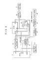
- the circuit arrangement of the electronic wrist- watch will be explained below in connection with Fig. 3.
- the electronic wristwatch operates based on an 8-bit parallel-processed microprogram control system, and a ROM (read-only memory) 11 stores a microprogram for controlling all the operations of the electronic wristwatch and delivers microinstruc- tions OP, DO and NA in a parallel fashion.
- the microinstruction OP is input to instruction decoder 12 where it is decoded.
- the output of instruction decoder 12 is fed as a read/write instruction to an R/W input terminal of RAM (random access memory) 13 and also as an arithmetic operation instruction to an "S" input terminal of ALU - (arithmetic and logic unit) 14.
- microinstruction DO of ROM is supplied as address data to an "Addr" input terminal of RAM 13, to a DI-2 input terminal of ALU 14 and to address control section 15, all via a data bus.
- Microinstruction NA of ROM 11 is next address data which is input to address control section 15.
- the output of address control section 15 is supplied to an Addr input terminal of ROM 11.
- RAM 13 includes, for example, an entry register and arithmetic operation register and is utilized for time count processing, key input processing, arithmetic operation processing, etc.
- RAM 13 executes data read/write operation under control of instruction decoder. Data which is read out from the DO output terminal of RAM 13 is supplied to "DI-1 and "DI-2" input terminals of ALU 14 and through display control section 16 to display section 17.
- ALU 14 performs various kinds of operations in accordance with an arithmetic operation instruction from instruction decoder 12. The result of calculation at ALU 14 is read into RAM 13 at the DI input terminal.
- ALU 14 upon the execution of a "judge" operation supplies a signal representing the presence or absence of the arithmetic operation data and signal representing the presence or absence of a carry generation, to address control section 15 to permit an address in ROM 11 to be converted.
- a time count clock of 16 Hz which is obtained by frequency dividing a reference clock signal from oscillator 18 by means of frequency divider 19, is input to address control section 15 and a time count processing is performed at a rate of one interruption per 1/16 second in accordance with the 16 Hz signal.
- a signal of a predetermined frequency which is output from frequency divider 19 is fed to timing generator 20.
- Timing generator 20 delivers various kinds of timing signals to the associated circuits.
- a key code which is output from key input section 21 is delivered to the DI 2 input terminal of ALU 14.
- Fig. 4 shows a memory mapping of a major portion of RAM 13.
- RAM 13 includes a memory area for permitting not only time count data and system control data, but also the other data to be freely written therein in accordance with key-in data.
- RAM 13 includes a BD register for counting a present date and storing it therein, BT register for counting a present time and storing it therein, and data memory.
- the data memory DM permits - schedule data of 50 pages corresponding to row addresses 1 to 50 to be stored therein.
- the respective row address areas permit schedule data comprised of month/date data, hour/minute time data and messages (the contents of the schedule) to be stored therein.
- the messages are stored in the areas M, to M 50 on a corresponding row; the date data is stored in the areas D, to D so ; and time data is stored in steps T, to T 50 in RAM 13.
- the respective row of the memory map in RAM 13 contains areas f, to f so for storing the next year data storing flags for the next year schedule.
- the - schedule data is, after being edited or rescheduled in a given sequence, stored in the data memory DM as set out below.
- RAM 13 includes an address register "n" for designating the row address in the data memory DM, memory N for a whole number of data on the schedule, display page pointer "P", flag register FS and ON/OFF flag register AL for alarm.
- step T is executed, waiting for a time count timing or for a key-in request.
- a key processing program is designated, executing a key processing or a display processing operation.
- step T3 When a time count clock of 16 Hz is output from frequency divider 19, the process is advanced to step T3 at which a time count processing is executed to permit present time data in the BT register in RAM 13 to be updated. As a result, if a date carry is obtained, the date data in the BD register is updated.
- an alarm processing is executed at step T 4 and a display processing is performed at step T s .
- Figs. 6A and 6B show detailed contents of the key processing and display processing at step T 2 in Fig. 5.
- the switch S3 is operated so as to perform a switching operation from the time-keeping mode to the schedule mode or from the - schedule mode to the time-keeping mode, this operation is detected at step T,, and the process goes to step T 12 .
- a judgment is made as to whether the contents of the register F s is "0" or not.
- the contents of the register F S is "1"
- the process goes to step T 13 and a mode switching is made between the time-keeping mode and the - schedule mode.
- no mode switching is performed.
- the setting mode is identified.
- the time display is made at step T 17 and for the schedule mode the value of the address register n is transferred to a display page pointer "P" and the schedule data corresponding to a page indicated by the value of the display page pointer P is read from the data memory DM for display (steps T, s and T 16 )
- the next announcement number is set in the address register "n".
- the row address of the data memory DM storing a specified schedule data corresponding to a page to be next announced is set to the address register n, noting that said data memory DM stores a plurality of - schedule data including said specified one. For this reason, that schedule data to be next announced is displayed on display section 17. This operation is repeated for each depression of the switch S 3 , permitting a cyclic switching to be made between the time-keeping mode and the schedule mode.
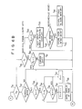
- Figs. 9A and 9B show the display switching states at that time, noting that Fig. 9A shows a time display in the time-keeping mode and Fig. 9B shows a schedule mode in the schedule mode.
- the time correction mode in Fig. 9C is obtained when the switch S 2 is operated in the normal mode in Fig. 9A.
- the normal mode is regained when the switch S, is operated in the time correction mode.
- step T 23 Only when upon the operation of the switch S 2 the time correction mode is switched over to the normal mode, the process goes to step T 23 , where an editing process is executed to permit a rearrangement, or reschedule of the schedule data as set forth later.
- step T 24 the time-of-day data is displayed.
- step T28 the value (the number to be next announced) of the address register n is transferred to the display page pointer P and the - schedule data of a page corresponding to the value of the display page pointer P is displayed (steps T 24 to T J o).
- step T 31 the process goes to step T 32 to examine whether or not the schedule mode is involved. If the time-keeping mode is involved, the switch S 4 becomes ineffective and, if in the schedule mode, a process attendant on the subsequent operation of the switch S 4 is executed.
- step T 33 a judgment is made as to whether the value of the whole data number memory N is "0" or not, i.e., whether no data is stored in the data memory DM.
- step T 34 the process goes to step T 34 at which the data of the display page pointer "P" and the value of the whole data number memory "N" are compared with each other. Now assume that the value of the display page pointer P is equal to the value of the whole data number memory N. Then the process goes to step T 35 at which a judgment is made as to whether the value of the whole data number memory is "50" or whether a full data state is reached at which the data corresponding to 50 pages are all stored in the data memory DM.
- step T 34 the display page number is detected as being smaller than the whole data number for schedule, data are sequentially stored in the data memory DM.
- step T 36 the value of the display page pointer P is incremented as in the form of P + 1 and the schedule data corresponding to a page indicated by the value of the display page pointer P is displayed (steps T 36 and T 38 ). Even where the display page number is equal to the whole data number but the data memory DM is not in the data full state, steps T 36 and T 38 are executed in which case a display is made as an empty page display. In this way, + 1 is added to the value of the whole page number pointer P through the operation of the switch S..
- step T 34 the display page number is greater than, or equal to the whole data number but the data memory DM is in the data full date, "1 " is set to the display page number pointer P to permit a first page to be displayed (steps T 37 and T 38 ).
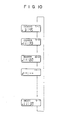
- Fig. 10 shows the states of display mode by the operation of the switch S 4 . Each time the switch S4 is operated the schedule data in the data memory DM is displayed in a cyclic fashion.
- step T 39 Upon the operation of the switch S, this operation is detected at step T 39 .
- the input data is stored as the schedule data in the data memory DM addressed by the value of the display page pointer P.
- the schedule data in the data memory DM can be corrected and new - schedule data can be written into the data memory DM.
- the data may be input thereto after the empty page has be displayed through the operation of the switch S 4 .
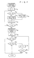
- Fig. 7 is a flowchart showing a detail of a - schedule data rearranging process (steps T 2 , and T 28 ) in Fig. 6.
- an initial value "1" " is set to the address register n (step T s ,) Then the process goes to step T 52 at which a comparison is made between the contents of the register BD and that of one (Dn) of areas D, to Dn designated by the contents D, to D so to examine whether or not a present date exceeds a preset date on the schedule. If it exceeds that preset date, the process goes to step T 53 at which, in order to show that said schedule data belongs in the next year, the next year flag is turned ON to permit "1" to be set to the area "fn" corresponding to the area Dn. If the present date does not exceed said preset date, the process goes to step T 54 at which the next year flag is turned OFF.
- step T55 + 1 is added to the value of the address register "n" in an incremental step. Then the process goes to step T 56 at which a comparison is made between the contents of the address register n and that of the whole data number memory N to see if the value of the address register n exceeds that whole data number. If it does not exceed the whole data number, the process T 52 goes back to step T 52 and the aforementioned operation is repeated. As a result, for the respective corresponding schedule data the next flag is turned ON or OFF in accordance with the present date.
- step T 57 at which the rearrangement, or reschedule of the schedule data is implemented. That is, on the basis of the present date and time the schedule data are rearranged, or rescheduled in a time order of recency. Stated in more detail, where there are a plurality of schedule data, they are rearranged in said time order and the next year schedule data are time-sequentially rearranged after the present year data.
- step T 59 a comparison is made between the contents of the area Dn and that of the register BD to see whether or not the present date reaches an initial schedule date. If the answer is in the negative, the value of the address register "n" remains to be "1", but when the preset schedule date is reached the process goes to step Too at which an examination is made as to whether or not the present time reaches the schedule time. If the answer is in the affirmative, the value of the address register "n" remains to be "1".
- Fig. 8 is a flowchart showing a detail of the alarm processing (step T,) shown in Fig. 5.
- the alarm flag is judged as being an ON or OFF state on the basis of the contents of the alarm flag register AL (step T 71 ).
- the alarm OFF a comparison is made between the present date and time data read out of the registers BD and BT and the schedule date and time data read out of memory areas Dn and step Tn which correspond to the next announcement number in the address register, and an examination is made as to whether or not there is an alarm time coincidence (step T n ).
- the alarm flag is turned ON and "1 " is set to the register AL, starting a timer counter operation (steps T73 and T 74 ). Simultaneously with the start of the timer a buzzer is turned ON, producing an alarm sound.
- the schedule data of a schedule corresponding to the alarm time coincidence is displayed in place of the time data.
- the - schedule data is displayed and simultaneously transferred to a voice synthesizing circuit (not shown in detail) so that this schedule data sounds as the synthesized voice. Alternatively, simply this schedule data sounds as the synthesized voice. If the alarm time is so reached the alarm flag is turned ON.
- step T7 When an alarm process is again started after 1/16 second, the process goes from step T7, to step T 75 at which a judgment is made as to whether or not a predetermined time is reached. If the answer is in the negative, an alarm sound continues until the predetermined time is reached, and at the same time the schedule data is displayed.
- step T76 the buzzer is turned OFF, stopping an alarm sound.
- step T77 the next announcement number is updated with + added to the value of the address register "n".
- a comparison is made between the present date and time data and the schedule date and time data corresponding to the updated address register "n". Where a coincidence occurs, as explained in connection with Fig. 8 an alarm sound is produced while at the same time the corresponding schedule is displayed. In addition the updating of the address register "n" is performed.
- the schedule data is rearranged in a time order of recency. Even if the schedule data are written in an irregular fashion, the respective schedule data is rearranged in the time order of recency with the present date and time as a reference. Since upon the detection of an alarm time coincidence it is only necessary to compares with the present time and date the schedule data indicated by the next announcement number in the address register "n", a process for detecting the alarm time can be efficiently performed even if a greater number of - schedule data are stored in the memory.
- Figs. 11 to 16 show another modification of this invention. The arrangement of this modification is the same as that set forth in connection with Figs. 1 to 10, except in the following respects.
- Fig. 11 shows another form of the display device of Fig. 2. In this form, in addition to digital display sections 2A and 2B and matrix display section 2C, display elements 101 through 114 are provided in a 2-row x 7-column dot matrix.
- the character "THIS” is, for example, printed as indicating "this week” for a corresponding row and character “NEXT” is, for example, printed as indicating "next week” with characters "S", "M”, ... "S” marked as Sunday, Monday, ... Saturday for the corresponding columns of the matrix array.
- display elements 101 to 114 are displayed through drivers L, to L,, when "1" is set to registers B, to B,, When the contents of registers B, to B, correspond to set schedule dates, "1 is stored in registers B, to B,4, noting that the setting operation is performed at steps T 4a to T 4d as shown in Fig. 13. That is, Fig.
- step T 4a a judgment is made as to whether or not a date carry is generated in the time count process of step T 3 . If the answer is in the affirmative, a detection is made as to whether or not the appointed day is Sunday. If said appointed day is Sunday, an alarm mark is set at step T 4 ,.
- the warning mark is so set that, for week days (including the appointed day i.e., Sunday) on which week schedule data are set, "1" is set to the registers B, to B, and that, for week days on which the next week schedule data are set, "1" is set to the registers B. to B,,.
- step T 4b If at step T 4b the appointed day is not Sunday, then "1" stored in the corresponding one of the register B, to B 14 is cancelled.
- the indication of the schedule displayed on the wrist-watch covers the two week schedule data. It is, of course, possible to display the more schedule indications than the two week schedule. Also, every time operations of the external operation switch, the schedule data succeeding to the "next week" schedule data may be sequentially displayed on the dot matrix display 2C as shown in Fig. 11.
- the schedule data were visually displayed on the display device 2.
- these schedule data may be printed out by a printer (not shown in detail).
- a key switch (not shown) is provided on this printer for entering data. Accordingly, it is very convenient to print out the schedule data succeeding to those entered by the key switch.
- this invention has been explained as having been applied to the wristwatch, it can be applied to the other type of time keeper, compact type electronic computer and the other electronic apparatus.
Landscapes
- Physics & Mathematics (AREA)
- General Physics & Mathematics (AREA)
- Electric Clocks (AREA)
- Calculators And Similar Devices (AREA)
- Management, Administration, Business Operations System, And Electronic Commerce (AREA)
Applications Claiming Priority (2)
| Application Number | Priority Date | Filing Date | Title |
|---|---|---|---|
| JP117750/85 | 1985-05-31 | ||
| JP60117750A JPS61275691A (ja) | 1985-05-31 | 1985-05-31 | アラ−ム時計 |
Publications (3)
| Publication Number | Publication Date |
|---|---|
| EP0204241A2 true EP0204241A2 (de) | 1986-12-10 |
| EP0204241A3 EP0204241A3 (en) | 1988-03-30 |
| EP0204241B1 EP0204241B1 (de) | 1991-08-21 |
Family
ID=14719389
Family Applications (1)
| Application Number | Title | Priority Date | Filing Date |
|---|---|---|---|
| EP86107113A Expired EP0204241B1 (de) | 1985-05-31 | 1986-05-26 | Elektronisches Uhrwerk mit Terminspeicher |
Country Status (5)
| Country | Link |
|---|---|
| US (1) | US4774697A (de) |
| EP (1) | EP0204241B1 (de) |
| JP (1) | JPS61275691A (de) |
| DE (1) | DE3680953D1 (de) |
| HK (1) | HK57996A (de) |
Families Citing this family (21)
| Publication number | Priority date | Publication date | Assignee | Title |
|---|---|---|---|---|
| US4866611A (en) * | 1987-01-29 | 1989-09-12 | International Business Machines Corporation | Method for automatically reconciling entries on two copies of independently maintained electronic calendars |
| US4868800A (en) * | 1988-11-23 | 1989-09-19 | Amihadar Arber | Advanced date warning system |
| US5303145A (en) * | 1990-12-26 | 1994-04-12 | International Business Machines Corporation | Method and apparatus for meeting confirmation in a data processing system |
| GB9324051D0 (en) * | 1993-11-23 | 1994-01-12 | Thomson Consumer Electronics | Adaptive battery charging system |
| US6039506A (en) * | 1997-09-08 | 2000-03-21 | Khachaturian; Jon E. | Method and apparatus for the offshore installation of multi-ton packages such as deck packages and jackets |
| JPH09288647A (ja) * | 1996-04-22 | 1997-11-04 | Sharp Corp | 情報処理装置 |
| US6209011B1 (en) | 1997-05-08 | 2001-03-27 | Microsoft Corporation | Handheld computing device with external notification system |
| US6996904B1 (en) | 1997-12-08 | 2006-02-14 | Micron Technology, Inc. | Method for managing cables |
| US6012683A (en) * | 1997-12-08 | 2000-01-11 | Micron Technology, Inc. | Apparatus for managing cables |
| US6038542A (en) * | 1998-04-28 | 2000-03-14 | Micron Electronics, Inc. | System for notifying an individual of a previously scheduled event |
| US6837618B1 (en) * | 1999-03-11 | 2005-01-04 | Citizen Watch Co., Ltd. | Electronic thermometer |
| US6502060B1 (en) | 1999-09-14 | 2002-12-31 | Petronics, Inc. | Pet chronometer and identification tag |
| US7178099B2 (en) * | 2001-01-23 | 2007-02-13 | Inxight Software, Inc. | Meta-content analysis and annotation of email and other electronic documents |
| US7212983B2 (en) | 2001-05-15 | 2007-05-01 | William Gibbens Redmann | Method and apparatus for providing visitors with a personalized itinerary and managed access to attractions |
| DE10313759B4 (de) * | 2003-03-27 | 2005-04-21 | Legrand Gmbh | Digitalschaltuhr mit grafischer Schaltanzeige |
| US7376909B1 (en) | 2003-08-11 | 2008-05-20 | Timothy P Coyle | Digital calendar |
| US20050073911A1 (en) * | 2003-10-06 | 2005-04-07 | Barnett Steven R. | Electronic prayer alert |
| US7345955B1 (en) * | 2004-06-01 | 2008-03-18 | Campbell Steven R | Display medium having a bibliographic reference corresponding to date |
| US7518955B2 (en) * | 2004-10-08 | 2009-04-14 | Nokia Corporation | Electronic device and method for enhancing usability of electronic device |
| WO2007030566A2 (en) * | 2005-09-09 | 2007-03-15 | Martin William R | Devices and methods directed to providing reminders to contact lens wearers |
| JP2011191497A (ja) * | 2010-03-15 | 2011-09-29 | Seiko Epson Corp | 電気泳動表示装置、電気泳動表示装置の駆動方法、電子機器 |
Family Cites Families (12)
| Publication number | Priority date | Publication date | Assignee | Title |
|---|---|---|---|---|
| US3999050A (en) * | 1975-10-10 | 1976-12-21 | Pitroda Satyan G | Electronic diary |
| JPS54101206A (en) * | 1978-01-26 | 1979-08-09 | Nissan Motor | Channel selection programming device for radio receiver |
| JPS54114058A (en) * | 1978-02-24 | 1979-09-05 | Sharp Corp | Electronic apparatus |
| JPS5533646A (en) * | 1978-08-31 | 1980-03-08 | Citizen Watch Co Ltd | Digital alarm watch |
| JPS5578175A (en) * | 1978-12-11 | 1980-06-12 | Nissan Motor Co Ltd | Ignition distributor for internal combustion engine |
| US4379339A (en) * | 1978-12-18 | 1983-04-05 | Tokyo Shibaura Denki Kabushiki Kaisha | Electronic timer |
| US4362392A (en) * | 1979-06-29 | 1982-12-07 | Sharp Kabushiki Kaisha | Electronic timepiece with message and/or alarm output capability |
| DE3039843A1 (de) * | 1979-10-22 | 1981-04-30 | Casio Computer Co., Ltd., Tokyo | Zeitanzeigevorrichtung |
| US4293845A (en) * | 1980-04-17 | 1981-10-06 | Villa Real Antony Euclid C | Electronic multi-patient medication-time-intake programmer and alarm system |
| GB2077465B (en) * | 1980-06-06 | 1984-07-04 | Casio Computer Co Ltd | Compact electronic device having calendar function |
| GB2090031B (en) * | 1980-12-09 | 1984-10-31 | Suwa Seikosha Kk | Electronic data storing apparatus |
| DE3214372A1 (de) * | 1982-04-20 | 1983-11-03 | Westdeutsche Elektrogerätebau GmbH, 4770 Soest | Elektronisches zeitschaltgeraet |
-
1985
- 1985-05-31 JP JP60117750A patent/JPS61275691A/ja active Granted
-
1986
- 1986-05-26 EP EP86107113A patent/EP0204241B1/de not_active Expired
- 1986-05-26 DE DE8686107113T patent/DE3680953D1/de not_active Expired - Lifetime
-
1988
- 1988-01-06 US US07/140,879 patent/US4774697A/en not_active Expired - Lifetime
-
1996
- 1996-04-03 HK HK57996A patent/HK57996A/en not_active IP Right Cessation
Also Published As
| Publication number | Publication date |
|---|---|
| US4774697A (en) | 1988-09-27 |
| EP0204241A3 (en) | 1988-03-30 |
| DE3680953D1 (de) | 1991-09-26 |
| EP0204241B1 (de) | 1991-08-21 |
| JPS61275691A (ja) | 1986-12-05 |
| JPH0346078B2 (de) | 1991-07-15 |
| HK57996A (en) | 1996-04-12 |
Similar Documents
| Publication | Publication Date | Title |
|---|---|---|
| US4774697A (en) | Electronic timepiece including a schedule memory device | |
| US5222209A (en) | Schedule displaying device | |
| US4158285A (en) | Interactive wristwatch calculator | |
| US4751668A (en) | Portable electronic memorandum device | |
| GB2040082A (en) | Multi-function electronic digital watch | |
| JP2984770B2 (ja) | 電子時計 | |
| JP3328815B2 (ja) | 時間割表示装置及び時間割表示制御方法 | |
| JPH0615313Y2 (ja) | デ−タ記憶装置 | |
| JPH0726760Y2 (ja) | アラーム時刻データ記憶装置 | |
| USRE34422E (en) | Portable electronic memorandum device | |
| JPS58137089A (ja) | タイムレコ−ダ | |
| JPH052877Y2 (de) | ||
| JPH0720634Y2 (ja) | 日付データ記憶装置 | |
| JPH0726761Y2 (ja) | データ記憶装置 | |
| JP2513600Y2 (ja) | デ―タバンク装置 | |
| JPH081475B2 (ja) | 印字機能付電子時計 | |
| JPH0434476Y2 (de) | ||
| JP2822456B2 (ja) | データ記憶装置 | |
| JPS6258191A (ja) | スケジユ−ル表示装置 | |
| US4192135A (en) | Portable electronic device | |
| JPH0710371Y2 (ja) | 時刻表表示装置 | |
| JPH0729516Y2 (ja) | 類別マーク付日付データ記憶装置 | |
| JPS61262678A (ja) | スケジユ−ル表示装置 | |
| JPS6040066B2 (ja) | カレンダ情報表示方式 | |
| JPH0434477Y2 (de) |
Legal Events
| Date | Code | Title | Description |
|---|---|---|---|
| PUAI | Public reference made under article 153(3) epc to a published international application that has entered the european phase |
Free format text: ORIGINAL CODE: 0009012 |
|
| AK | Designated contracting states |
Kind code of ref document: A2 Designated state(s): CH DE FR GB LI |
|
| PUAL | Search report despatched |
Free format text: ORIGINAL CODE: 0009013 |
|
| AK | Designated contracting states |
Kind code of ref document: A3 Designated state(s): CH DE FR GB LI |
|
| 17P | Request for examination filed |
Effective date: 19880909 |
|
| 17Q | First examination report despatched |
Effective date: 19900320 |
|
| GRAA | (expected) grant |
Free format text: ORIGINAL CODE: 0009210 |
|
| AK | Designated contracting states |
Kind code of ref document: B1 Designated state(s): CH DE FR GB LI |
|
| REF | Corresponds to: |
Ref document number: 3680953 Country of ref document: DE Date of ref document: 19910926 |
|
| ET | Fr: translation filed | ||
| PLBE | No opposition filed within time limit |
Free format text: ORIGINAL CODE: 0009261 |
|
| STAA | Information on the status of an ep patent application or granted ep patent |
Free format text: STATUS: NO OPPOSITION FILED WITHIN TIME LIMIT |
|
| 26N | No opposition filed | ||
| PGFP | Annual fee paid to national office [announced via postgrant information from national office to epo] |
Ref country code: FR Payment date: 20010518 Year of fee payment: 16 |
|
| PGFP | Annual fee paid to national office [announced via postgrant information from national office to epo] |
Ref country code: DE Payment date: 20010522 Year of fee payment: 16 |
|
| PGFP | Annual fee paid to national office [announced via postgrant information from national office to epo] |
Ref country code: CH Payment date: 20010529 Year of fee payment: 16 |
|
| REG | Reference to a national code |
Ref country code: GB Ref legal event code: IF02 |
|
| PG25 | Lapsed in a contracting state [announced via postgrant information from national office to epo] |
Ref country code: LI Free format text: LAPSE BECAUSE OF NON-PAYMENT OF DUE FEES Effective date: 20020531 Ref country code: CH Free format text: LAPSE BECAUSE OF NON-PAYMENT OF DUE FEES Effective date: 20020531 |
|
| PG25 | Lapsed in a contracting state [announced via postgrant information from national office to epo] |
Ref country code: DE Free format text: LAPSE BECAUSE OF NON-PAYMENT OF DUE FEES Effective date: 20021203 |
|
| REG | Reference to a national code |
Ref country code: CH Ref legal event code: PL |
|
| PG25 | Lapsed in a contracting state [announced via postgrant information from national office to epo] |
Ref country code: FR Free format text: LAPSE BECAUSE OF NON-PAYMENT OF DUE FEES Effective date: 20030131 |
|
| REG | Reference to a national code |
Ref country code: FR Ref legal event code: ST |
|
| PGFP | Annual fee paid to national office [announced via postgrant information from national office to epo] |
Ref country code: GB Payment date: 20050525 Year of fee payment: 20 |
|
| PG25 | Lapsed in a contracting state [announced via postgrant information from national office to epo] |
Ref country code: GB Free format text: LAPSE BECAUSE OF EXPIRATION OF PROTECTION Effective date: 20060525 |
|
| REG | Reference to a national code |
Ref country code: GB Ref legal event code: PE20 |