EP0212251A2 - Procédé utilisant une attaque sèche pour éviter un cycle de masquage et d'attaque - Google Patents
Procédé utilisant une attaque sèche pour éviter un cycle de masquage et d'attaque Download PDFInfo
- Publication number
- EP0212251A2 EP0212251A2 EP86109712A EP86109712A EP0212251A2 EP 0212251 A2 EP0212251 A2 EP 0212251A2 EP 86109712 A EP86109712 A EP 86109712A EP 86109712 A EP86109712 A EP 86109712A EP 0212251 A2 EP0212251 A2 EP 0212251A2
- Authority
- EP
- European Patent Office
- Prior art keywords
- etching
- layer
- dielectric layer
- mask
- dry etchant
- Prior art date
- Legal status (The legal status is an assumption and is not a legal conclusion. Google has not performed a legal analysis and makes no representation as to the accuracy of the status listed.)
- Granted
Links
Images
Classifications
-
- H—ELECTRICITY
- H10—SEMICONDUCTOR DEVICES; ELECTRIC SOLID-STATE DEVICES NOT OTHERWISE PROVIDED FOR
- H10P—GENERIC PROCESSES OR APPARATUS FOR THE MANUFACTURE OR TREATMENT OF DEVICES COVERED BY CLASS H10
- H10P50/00—Etching of wafers, substrates or parts of devices
- H10P50/20—Dry etching; Plasma etching; Reactive-ion etching
- H10P50/28—Dry etching; Plasma etching; Reactive-ion etching of insulating materials
- H10P50/282—Dry etching; Plasma etching; Reactive-ion etching of insulating materials of inorganic materials
- H10P50/283—Dry etching; Plasma etching; Reactive-ion etching of insulating materials of inorganic materials by chemical means
-
- C—CHEMISTRY; METALLURGY
- C03—GLASS; MINERAL OR SLAG WOOL
- C03C—CHEMICAL COMPOSITION OF GLASSES, GLAZES OR VITREOUS ENAMELS; SURFACE TREATMENT OF GLASS; SURFACE TREATMENT OF FIBRES OR FILAMENTS MADE FROM GLASS, MINERALS OR SLAGS; JOINING GLASS TO GLASS OR OTHER MATERIALS
- C03C15/00—Surface treatment of glass, not in the form of fibres or filaments, by etching
Definitions
- This invention relates to a process for simultaneously etching holes in both thick and thin portions of a dielectric layer on a semiconductor substrate. More particularly, the process is used to eliminate a mask-and-etch cycle in the manufacturing of integrated circuits.
- the etching of dielectric layers on a semiconductor substrate is critical to the manufacture of integrated circuits. Repeated masking and etching cycles of the dielectric layers are used to define the minute structural patterns of the integrated circuit devices. Wet etching processes are the conventional etching processes used. These processes etch isotropically. Therefore, significant lateral, as well as vertical, etching occurs during processing.
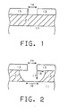
- the conventional wet etching of a dielectric layer 12 on a semiconductor substrate 11 is illustrated in Figs. 1 and 2.
- the area of dielectric layer 12 to be etched is defined by a window 14 in a conventional photolithographic mask 13. Upon exposure of dielectric layer 12 to wet etching, an area 16 of semiconductor substrate 11 is exposed.
- the size of area 16 is a function of the size of window 14, the amount of vertical etching, and the amount of lateral etching that occurs in dielectric layer 12.
- Wet etching is required for a long enough time to ensure complete vertical etching 17 of dielectric layer 12, yet the etching time must be minimized to avoid excessive lateral etching 18.
- Excessive lateral etching results in the increased size of area 16, thereby making maintenance of the dimensional tolerances required more difficult.
- the window in the mask overlying the dielectric layer cannot be made smaller, the excessive lateral etching may make it impossible to meet the required dimensional tolerances.
- the mask window may already be of the smallest size possible within the limits of existing technology, making the simultaneous etching of both the thick and thin portions of the dielectric layer impractical.
- the object of this invention is to provide an improved process for simultaneously etching both the thick and thin portions of a dielectric layer on a semiconductor substrate while minimizing lateral etching.
- This process employs an anisotropic dry etchant.
- the dielectric layer is masked allowing for windows over both the thick and thin portions of the layer.
- the dielectric layer is then exposed to the anisotropic dry etchant through the mask windows until the dielectric layer in each window is etched down to the semiconductor substrate. Because no significant lateral etching occurs, dimensional tolerances are easily maintained.
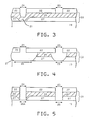
- Fig. 3 shows a silicon substrate 19 with both thick and thin portions 20, 21 of a dielectric layer thereon.
- Thin portion 21 is phosphosilicate glass 28.
- Thick portion 20 includes composite layers of silicon dioxide 27 and phosphosilicate glass (hereinafter referred to as PSG) 28.
- Window 23 in mask 22 exposes the surface of the thick portion 20 of the dielectric layer.
- Window 24 in mask 22 exposes the surface of the thin portion 21 of the dielectric layer.
- Masking may be accomplished by any conventional technique, such as photolithography.
- silicon substrate 19 and portions 20 and 21 of the dielectric layer are shown after exposure to a wet etchant such as dilute hydrofluoric acid.
- a wet etchant such as dilute hydrofluoric acid.
- the wet etchant consumed thick and thin portions 20, 21 of the dielectric layer through windows 23 and 24 until areas 25 and 26 of the silicon substrate were exposed.
- the excess time required to complete vertical etching of thick portion 20 of the dielectric layer resulted in significant lateral etching of thin portion 21 of the dielectric layer.
- the lateral etching resulted in an expanded area 26 with potentially disastrous results if dimensional tolerances are not maintained.
- Fig. 5 shows the same structure as shown in Fig. 4 except that the wet etchant used was replaced by an anisotropic dry etchant.
- An example of such a dry etchant is a mixture of gaseous hydrogen and carbon tetrafluoride containing 29% to 35% hydrogen by volume.
- the etchant can be used in the reactive ion etch mode under the conditions of 38.6 ⁇ bar of pressure and 0.58 watts/cm-cm power density. Any conventional parallel plate dry etching apparatus can be used. Similar to the wet etch process, the dry etchant consumed the dielectric layer through windows 23 and 24 until areas 25 and 26a of the silicon substrate were exposed.
- the material requirements of the process invention are relative. Although a mixture of hydrogen and carbontetrafluoride has been identified, other dry etching compositions may be used.
- the substrate may be composed of silicon or other materials, such as germanium or gallium arsenide.
- the layer to be etched may be comprised of composite layers of silicon dioxide and PSG as mentioned, or either silicon dioxide or PSG alone, or yet other individual or composite layer materials.
- the mask may be a conventional photoresist, or other applicable materials.
- the significant requirement is that the dry etchant selectively etch the layer relative to the substrate and mask at a ratio of at least 20 to 1. Furthermore, the dry etchant must consume the layer anisotropically.
- Anisotropic etching refers to a rate of vertical etching at least 15 times greater than the rate of lateral etching.
Landscapes
- Chemical & Material Sciences (AREA)
- Life Sciences & Earth Sciences (AREA)
- Engineering & Computer Science (AREA)
- Chemical Kinetics & Catalysis (AREA)
- General Chemical & Material Sciences (AREA)
- Geochemistry & Mineralogy (AREA)
- Materials Engineering (AREA)
- Organic Chemistry (AREA)
- Drying Of Semiconductors (AREA)
- Electrodes Of Semiconductors (AREA)
- Weting (AREA)
Applications Claiming Priority (2)
| Application Number | Priority Date | Filing Date | Title |
|---|---|---|---|
| US764148 | 1985-08-09 | ||
| US06/764,148 US4624739A (en) | 1985-08-09 | 1985-08-09 | Process using dry etchant to avoid mask-and-etch cycle |
Publications (3)
| Publication Number | Publication Date |
|---|---|
| EP0212251A2 true EP0212251A2 (fr) | 1987-03-04 |
| EP0212251A3 EP0212251A3 (en) | 1988-03-16 |
| EP0212251B1 EP0212251B1 (fr) | 1991-10-16 |
Family
ID=25069822
Family Applications (1)
| Application Number | Title | Priority Date | Filing Date |
|---|---|---|---|
| EP86109712A Expired - Lifetime EP0212251B1 (fr) | 1985-08-09 | 1986-07-15 | Procédé utilisant une attaque sèche pour éviter un cycle de masquage et d'attaque |
Country Status (4)
| Country | Link |
|---|---|
| US (1) | US4624739A (fr) |
| EP (1) | EP0212251B1 (fr) |
| JP (1) | JPS6237936A (fr) |
| DE (1) | DE3681994D1 (fr) |
Families Citing this family (12)
| Publication number | Priority date | Publication date | Assignee | Title |
|---|---|---|---|---|
| FR2593631B1 (fr) * | 1986-01-27 | 1989-02-17 | Maurice Francois | Ecran d'affichage a matrice active a resistance de grille et procedes de fabrication de cet ecran |
| US5010039A (en) * | 1989-05-15 | 1991-04-23 | Ku San Mei | Method of forming contacts to a semiconductor device |
| US5205902A (en) * | 1989-08-18 | 1993-04-27 | Galileo Electro-Optics Corporation | Method of manufacturing microchannel electron multipliers |
| US5086248A (en) * | 1989-08-18 | 1992-02-04 | Galileo Electro-Optics Corporation | Microchannel electron multipliers |
| KR100797202B1 (ko) * | 2000-06-23 | 2008-01-23 | 허니웰 인터내셔널 인코포레이티드 | 손상된 실리카 유전 필름에 소수성을 부여하는 방법 및 손상된 실리카 유전 필름 처리 방법 |
| US6638438B2 (en) * | 2001-10-16 | 2003-10-28 | Ulisatera Corporation | Printed circuit board micro hole processing method |
| US7709371B2 (en) * | 2003-01-25 | 2010-05-04 | Honeywell International Inc. | Repairing damage to low-k dielectric materials using silylating agents |
| WO2004068555A2 (fr) * | 2003-01-25 | 2004-08-12 | Honeywell International Inc | Reparation et restauration de materiaux et de films dielectriques endommages |
| US7154086B2 (en) * | 2003-03-19 | 2006-12-26 | Burle Technologies, Inc. | Conductive tube for use as a reflectron lens |
| US8475666B2 (en) * | 2004-09-15 | 2013-07-02 | Honeywell International Inc. | Method for making toughening agent materials |
| US7678712B2 (en) * | 2005-03-22 | 2010-03-16 | Honeywell International, Inc. | Vapor phase treatment of dielectric materials |
| US20080073516A1 (en) * | 2006-03-10 | 2008-03-27 | Laprade Bruce N | Resistive glass structures used to shape electric fields in analytical instruments |
Family Cites Families (11)
| Publication number | Priority date | Publication date | Assignee | Title |
|---|---|---|---|---|
| US4180432A (en) * | 1977-12-19 | 1979-12-25 | International Business Machines Corporation | Process for etching SiO2 layers to silicon in a moderate vacuum gas plasma |
| US4253907A (en) * | 1979-03-28 | 1981-03-03 | Western Electric Company, Inc. | Anisotropic plasma etching |
| JPS5690525A (en) * | 1979-11-28 | 1981-07-22 | Fujitsu Ltd | Manufacture of semiconductor device |
| DE3016736A1 (de) * | 1980-04-30 | 1981-11-05 | Siemens AG, 1000 Berlin und 8000 München | Verfahren zum herstellen geaetzter strukturen in siliziumoxidschichten |
| JPS5796552A (en) * | 1980-12-09 | 1982-06-15 | Nec Corp | Manufacture of semiconductor device |
| US4457820A (en) * | 1981-12-24 | 1984-07-03 | International Business Machines Corporation | Two step plasma etching |
| DE3216823A1 (de) * | 1982-05-05 | 1983-11-10 | Siemens AG, 1000 Berlin und 8000 München | Verfahren zum herstellen von strukturen von aus metallsilizid und polysilizium bestehenden doppelschichten auf integrierte halbleiterschaltungen enthaltenden substraten durch reaktives ionenaetzen |
| DE3315719A1 (de) * | 1983-04-29 | 1984-10-31 | Siemens AG, 1000 Berlin und 8000 München | Verfahren zum herstellen von strukturen von aus metallsiliziden bzw. silizid-polysilizium bestehenden doppelschichten fuer integrierte halbleiterschaltungen durch reaktives ionenaetzen |
| US4508815A (en) * | 1983-11-03 | 1985-04-02 | Mostek Corporation | Recessed metallization |
| US4532002A (en) * | 1984-04-10 | 1985-07-30 | Rca Corporation | Multilayer planarizing structure for lift-off technique |
| JPS61161721A (ja) * | 1985-01-11 | 1986-07-22 | Nec Corp | 表面平坦化法 |
-
1985
- 1985-08-09 US US06/764,148 patent/US4624739A/en not_active Expired - Lifetime
-
1986
- 1986-07-07 JP JP61158129A patent/JPS6237936A/ja active Granted
- 1986-07-15 EP EP86109712A patent/EP0212251B1/fr not_active Expired - Lifetime
- 1986-07-15 DE DE8686109712T patent/DE3681994D1/de not_active Expired - Lifetime
Also Published As
| Publication number | Publication date |
|---|---|
| JPS6237936A (ja) | 1987-02-18 |
| US4624739A (en) | 1986-11-25 |
| EP0212251B1 (fr) | 1991-10-16 |
| DE3681994D1 (de) | 1991-11-21 |
| JPH0545057B2 (fr) | 1993-07-08 |
| EP0212251A3 (en) | 1988-03-16 |
Similar Documents
| Publication | Publication Date | Title |
|---|---|---|
| US4624739A (en) | Process using dry etchant to avoid mask-and-etch cycle | |
| GB1194159A (en) | Improvements relating to Integrated Circuits. | |
| CA1187211A (fr) | Masque-ecran amovible | |
| US3922184A (en) | Method for forming openings through insulative layers in the fabrication of integrated circuits | |
| JPS57130431A (en) | Manufacture of semiconductor device | |
| JPS6469031A (en) | Manufacture of semiconductor device | |
| JPS56122143A (en) | Manufacture of semiconductor device | |
| JPS6191929A (ja) | ドライエツチング方法 | |
| JPS55128830A (en) | Method of working photoresist film | |
| JPS57136327A (en) | Etching method | |
| JPS54162490A (en) | Manufacture of semiconductor device | |
| JPS57137472A (en) | Etching method for polycrystalline silicon | |
| JPS57169259A (en) | Manufacture of semiconductor device | |
| JPS5691446A (en) | Forming of element segregation region of semiconductor integrated circuit | |
| JPS63213930A (ja) | 半導体装置の製造方法 | |
| JP2811724B2 (ja) | エッチング方法 | |
| JPS5769745A (en) | Manufacture of semiconductor device | |
| JPS6420641A (en) | Manufacture of semiconductor device | |
| JPS5758321A (en) | Manufacture of semiconductor device | |
| JPH01243426A (ja) | レジスト膜のエツチング方法 | |
| JPS6473718A (en) | Manufacture of semiconductor integrated circuit device | |
| JPH03296217A (ja) | 半導体装置の製造方法 | |
| JPS5743431A (en) | Manufacture of semiconductor device | |
| KR19990021583A (ko) | 반도체 장치의 패턴 형성 방법 | |
| JPS55163863A (en) | Formation of wiring pattern |
Legal Events
| Date | Code | Title | Description |
|---|---|---|---|
| PUAI | Public reference made under article 153(3) epc to a published international application that has entered the european phase |
Free format text: ORIGINAL CODE: 0009012 |
|
| AK | Designated contracting states |
Kind code of ref document: A2 Designated state(s): DE FR GB |
|
| 17P | Request for examination filed |
Effective date: 19870623 |
|
| PUAL | Search report despatched |
Free format text: ORIGINAL CODE: 0009013 |
|
| AK | Designated contracting states |
Kind code of ref document: A3 Designated state(s): DE FR GB |
|
| 17Q | First examination report despatched |
Effective date: 19900327 |
|
| GRAA | (expected) grant |
Free format text: ORIGINAL CODE: 0009210 |
|
| AK | Designated contracting states |
Kind code of ref document: B1 Designated state(s): DE FR GB |
|
| REF | Corresponds to: |
Ref document number: 3681994 Country of ref document: DE Date of ref document: 19911121 |
|
| ET | Fr: translation filed | ||
| PGFP | Annual fee paid to national office [announced via postgrant information from national office to epo] |
Ref country code: GB Payment date: 19920624 Year of fee payment: 7 |
|
| PLBE | No opposition filed within time limit |
Free format text: ORIGINAL CODE: 0009261 |
|
| STAA | Information on the status of an ep patent application or granted ep patent |
Free format text: STATUS: NO OPPOSITION FILED WITHIN TIME LIMIT |
|
| 26N | No opposition filed | ||
| PG25 | Lapsed in a contracting state [announced via postgrant information from national office to epo] |
Ref country code: FR Effective date: 19930331 |
|
| PG25 | Lapsed in a contracting state [announced via postgrant information from national office to epo] |
Ref country code: DE Effective date: 19930401 |
|
| REG | Reference to a national code |
Ref country code: FR Ref legal event code: ST |
|
| PG25 | Lapsed in a contracting state [announced via postgrant information from national office to epo] |
Ref country code: GB Effective date: 19930715 |
|
| GBPC | Gb: european patent ceased through non-payment of renewal fee |
Effective date: 19930715 |