EP0212836B1 - Strahlungsdarstellungseinrichtung - Google Patents
Strahlungsdarstellungseinrichtung Download PDFInfo
- Publication number
- EP0212836B1 EP0212836B1 EP86305390A EP86305390A EP0212836B1 EP 0212836 B1 EP0212836 B1 EP 0212836B1 EP 86305390 A EP86305390 A EP 86305390A EP 86305390 A EP86305390 A EP 86305390A EP 0212836 B1 EP0212836 B1 EP 0212836B1
- Authority
- EP
- European Patent Office
- Prior art keywords
- component
- scintillator
- detector
- radiation
- output signal
- Prior art date
- Legal status (The legal status is an assumption and is not a legal conclusion. Google has not performed a legal analysis and makes no representation as to the accuracy of the status listed.)
- Expired
Links
- 230000005855 radiation Effects 0.000 title claims description 36
- 238000003384 imaging method Methods 0.000 title claims description 7
- 239000000463 material Substances 0.000 claims description 16
- 238000002591 computed tomography Methods 0.000 claims description 7
- 229910052793 cadmium Inorganic materials 0.000 claims description 5
- BDOSMKKIYDKNTQ-UHFFFAOYSA-N cadmium atom Chemical compound [Cd] BDOSMKKIYDKNTQ-UHFFFAOYSA-N 0.000 claims description 5
- PBYZMCDFOULPGH-UHFFFAOYSA-N tungstate Chemical compound [O-][W]([O-])(=O)=O PBYZMCDFOULPGH-UHFFFAOYSA-N 0.000 claims description 5
- XQPRBTXUXXVTKB-UHFFFAOYSA-M caesium iodide Chemical compound [I-].[Cs+] XQPRBTXUXXVTKB-UHFFFAOYSA-M 0.000 claims description 3
- 230000001902 propagating effect Effects 0.000 claims description 2
- 239000002344 surface layer Substances 0.000 claims 2
- 229910052797 bismuth Inorganic materials 0.000 claims 1
- JCXGWMGPZLAOME-UHFFFAOYSA-N bismuth atom Chemical compound [Bi] JCXGWMGPZLAOME-UHFFFAOYSA-N 0.000 claims 1
- 239000010410 layer Substances 0.000 claims 1
- 239000002356 single layer Substances 0.000 claims 1
- 239000013078 crystal Substances 0.000 description 7
- 238000000034 method Methods 0.000 description 4
- 238000011144 upstream manufacturing Methods 0.000 description 4
- 238000006243 chemical reaction Methods 0.000 description 3
- 238000001228 spectrum Methods 0.000 description 3
- 238000001514 detection method Methods 0.000 description 2
- 230000000694 effects Effects 0.000 description 2
- 230000001965 increasing effect Effects 0.000 description 2
- 238000005259 measurement Methods 0.000 description 2
- 239000006096 absorbing agent Substances 0.000 description 1
- 238000010521 absorption reaction Methods 0.000 description 1
- 230000005540 biological transmission Effects 0.000 description 1
- 238000013170 computed tomography imaging Methods 0.000 description 1
- 230000002708 enhancing effect Effects 0.000 description 1
- 150000002500 ions Chemical class 0.000 description 1
- 229910052710 silicon Inorganic materials 0.000 description 1
- 239000010703 silicon Substances 0.000 description 1
Images


Classifications
-
- G—PHYSICS
- G01—MEASURING; TESTING
- G01T—MEASUREMENT OF NUCLEAR OR X-RADIATION
- G01T1/00—Measuring X-radiation, gamma radiation, corpuscular radiation, or cosmic radiation
- G01T1/16—Measuring radiation intensity
- G01T1/20—Measuring radiation intensity with scintillation detectors
- G01T1/202—Measuring radiation intensity with scintillation detectors the detector being a crystal
-
- G—PHYSICS
- G01—MEASURING; TESTING
- G01T—MEASUREMENT OF NUCLEAR OR X-RADIATION
- G01T1/00—Measuring X-radiation, gamma radiation, corpuscular radiation, or cosmic radiation
- G01T1/16—Measuring radiation intensity
- G01T1/20—Measuring radiation intensity with scintillation detectors
- G01T1/2018—Scintillation-photodiode combinations
- G01T1/20183—Arrangements for preventing or correcting crosstalk, e.g. optical or electrical arrangements for correcting crosstalk
Definitions
- the present invention relates to radiation imaging systems e.g. for computed tomography imaging.
- a two dimensional image is generated from multiple one dimensional projections.
- a source of radiation e.g. x-radiation
- the x-ray tube radiation source used in computed tomography emits x-ray photons over polychromatic or continuous energy spectrum which extends from near zero in energy to a maximum which is determined by the voltage (kv) applied to the source.
- the performance and energy spectra of x-ray tubes is well understood and documented by those of ordinary skill in the relevant art.
- the radiation detectors utilized in computed tomography each produce a signal proportional to the total x-ray energy absorbed by the detector.
- the lower energy x-ray photons striking a detector contribute a relatively small amount to the total output signal of the detector, whereas the higher energy photons incident on the detector produce correspondingly larger contributions to the output signal.
- the low energy x-ray photons are more readily absorbed in the patient, while the high energy photons have a greater tendency to pass through the patient's body and to undergo less attenuation than do the low energy x-ray photons.
- the low energy radiation contains more contrast information defining the patienfs internal body structure than does the high energy radiation, which more uniformly passes through the patient's body, as a result of less attenuation.
- the detector output signal is more a function of the high energy radiation, which carries relatively less contrast information, than it is a function of the lower energy radiation which is relatively rich in image information. Accordingly, the present detectors that employ a single energy sensitive element (e.g., a single scintillation crystal or a gas filled ion chamber) weights its output signal in favor of the less informative high energy radiation than in favor of the more informative low energy radiation.
- a single energy sensitive element e.g., a single scintillation crystal or a gas filled ion chamber
- the generation of x-ray photons by an x-ray tube anode is a random process. Even where the x-ray tube kV and mA (voltage and current) are held constant, the number of photons emitted from the anode fluctuates statistically in time about an average value with a Poisson probability distribution.
- the absorption, or attenuation, of the x-ray photons in matter, such as in a patient's body, is also a random process following similar laws of probability theory. Therefore, the number of photons detected during a fixed time period, with all other conditions held constant, will vary from one measurement to the next. This statistical fluctuation in the measurement gives rise to an uncertainty or ambiguity in the true value of the attenuation.
- Quantum noise This ambiguity is sometimes referred to as “quantum noise” or “quantum statistics”. While this quantum noise sets an absolute, or fundamental limit on the quality of an image that can ultimately be obtained, unequal response by the detector to photons of different energies magnifies this noise problem.
- Case I is 17% noisier than Case II.
- the number of detected photons i.e., N, would have to be increased to 136. This would correspond to an increase in patient dose of 36%.
- a radiation imaging system comprising: a radiation source for propagating radiation along a path ; a detector assembly in said radiation path for producing an analog output signal in response to said radiation, said detector assembly comprising first and second scintillator components preferentially responsive to lower and higher energy components of said radiation respectively and a detector component for producing said output signal in response to the responses of said first and second scintillator components to said radiation ; and imaging circuitry responsive to said output signal, said first and second scintillator detector assembly components comprising scintillation material and said detector component comprising a detector for scintillation produced by said material, said first and second scintillator detector assembly components being arranged serially along said radiation path with said first scintillator detector assembly component nearer said source and having a higher photon to light conversion efficiency than said second scintillator detector assembly component, characterised in that said detector component is disposed along said radiation path between said first scintillator component and said source thereby to enhance a
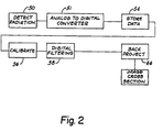
- a radiation imaging system com- console 14 (figure 1).
- An important purpose of this invention is the provision of improved embodiments for the detectors, having enhanced response to lower energy radiation and which reduce the noise resulting from the statistical variations of the radiation photons.
- An important feature of the invention involves increasing the weighting, or detector output signal contribution of the lower energy x-ray photons relative to the weighting or signal contribution of the higher energy photons.
- Such a radiation detector will produce an output signal which is lower in noise and higher in information content than could be produced by prior art detectors.
- One such detector comprises a scintillator including a sandwich of two or more layers of scintillation material having different energy conversion efficiency characteristics.
- the geometry of such a detector 100 is such that radiation from the source first impinges upon a first layer 102 of scintillation material, such as cesium iodide, of thickness 0.2 mm, having a relatively high efficiency in converting x-ray photons to light photons.
- the lower energy x-ray photons tend to be preferentially absorbed, while the higher energy photons tend to pass through the layer 102 and to be absorbed in a layer 104 which comprises a scintillation material, such as cadmium tungstate, of thickness 2.0 mm, having a relatively lower efficiency in converting x-ray photons to light photons.
- the interface between the layers 102, 104 is at least partially light transmissive.
- the light scintillations from both the layers 102, 104 are detected by a photodiode 106, which views both layers simultaneously, and produces an analog electrical output signal on a lead 108 which is a function of the detected analog scintillations from both layers.
- the component of the analog output signal, appearing at the lead 108 which is due to the lower energy photons, has enhanced weighting relative to the contribution attributable to the higher energy x-ray photons striking the detector. That is, the signal at the lead 108 has a relatively enhanced component which comprises a contribution resultant upon the conversion to light energy of the lower energy x-ray photons, compared to the results obtained in prior art detectors having only a single crystal upstream of the photodiode in the x-ray path.
- the enhancement of the response of the output 108 due to lower energy x-ray photons renders the signal appearing at the output 108 more independent of random photon fluctuations of the incident x-ray energy than would be the case if only the lower efficiency crystal 104 were used. This is because the high and low energy components of the analog output signal at 108 are more nearly equal, for a polyenergetic spectrum, when the weighting of the lower energy contribution is enhanced.
- Figure 4 shows a first detector in accordance with the present invention which achieves enhanced weighting of the detector response to the lower energy x-ray photons and includes a single relatively thick scintillator layer 110 and a single photodiode 112.
- the photodiode is positioned upstream in the x-ray path with respect to the crystal 110.
- x-rays transmitted through the subject first pass through the relatively thin photodiode 112, and are then absorbed in the crystal 110.
- the lower energy x-ray photons are preferentially absorbed, and converted to light photons, in the region of the layer 110 near its upstream surface 116.
- the higher energy x-ray photons are converted to light photons generally more near the lower, or downstream, surface 118 of the layer 110.
- the light photons resulting from the lower energy x-ray photons are preferentially converted to light scintillations nearer the photodiode 112 than are the scintillations resulting from the higher energy x-ray photons.
- the higher energy photons tend to penetrate further through the layer 110, before being converted to light scintillations, than do the lower energy x-ray photons. Therefore, the photodiode 112 will respond more strongly to the scintillations near the surface 116 than to those near the surface 118, due to the fact that the scintillations near the surface 116 are closer to the photodiode than those further away near the surface 118.
- the photodiode 112 comprises an epitaxially grown layer of silicon.
- the scintillation layer 110 comprises a portion of semi-transparent crystal, for example cadmium tungstate, and has a thickness of about 2 mm.
- the semi-transparency of the layer 110 helps to exaggerate the attenuation of the response of the photodiode 112 to more distant scintillations occurring near the surface 118, to assist in further enhancing the weighting of the low energy response in the output signal at the lead 114.
- Figure 5 shows a second detector in accordance with the present invention incorporating a sandwich crystalline layer assembly 120, 122, in combination with a photodiode 124.
- the photodiode 124 is positioned relatively upstream in the x-ray path, and receives incident x-rays prior to the crystalline layers.
- the incident x-rays first penetrate the photodiode 124, which is substantially transparent to x-ray, and are absorbed in the layers 120,122.
- the layer 120 comprises a high efficiency absorber, such as cesium iodide, of thickness 0.2 mm, which preferentially absorbs and converts to light lower energy x-ray photons.
- the layer 122 comprises a material having nent of said radiation.
Landscapes
- Physics & Mathematics (AREA)
- Health & Medical Sciences (AREA)
- Life Sciences & Earth Sciences (AREA)
- General Physics & Mathematics (AREA)
- High Energy & Nuclear Physics (AREA)
- Molecular Biology (AREA)
- Spectroscopy & Molecular Physics (AREA)
- Chemical & Material Sciences (AREA)
- Crystallography & Structural Chemistry (AREA)
- Measurement Of Radiation (AREA)
- Apparatus For Radiation Diagnosis (AREA)
- Analysing Materials By The Use Of Radiation (AREA)
Claims (16)
Applications Claiming Priority (2)
| Application Number | Priority Date | Filing Date | Title |
|---|---|---|---|
| US77042985A | 1985-08-29 | 1985-08-29 | |
| US770429 | 1985-08-29 |
Publications (2)
| Publication Number | Publication Date |
|---|---|
| EP0212836A1 EP0212836A1 (de) | 1987-03-04 |
| EP0212836B1 true EP0212836B1 (de) | 1991-03-13 |
Family
ID=25088512
Family Applications (1)
| Application Number | Title | Priority Date | Filing Date |
|---|---|---|---|
| EP86305390A Expired EP0212836B1 (de) | 1985-08-29 | 1986-07-14 | Strahlungsdarstellungseinrichtung |
Country Status (4)
| Country | Link |
|---|---|
| EP (1) | EP0212836B1 (de) |
| JP (1) | JP2540033B2 (de) |
| CA (1) | CA1260160A (de) |
| DE (1) | DE3678065D1 (de) |
Families Citing this family (8)
| Publication number | Priority date | Publication date | Assignee | Title |
|---|---|---|---|---|
| FR2621705B1 (fr) * | 1987-10-09 | 1990-03-30 | Thomson Csf | Detecteur multiradiations, notamment detecteur de rayons x a double energie |
| EP0378896A3 (de) * | 1988-11-23 | 1991-05-22 | Picker International, Inc. | Strahlungsdetektoren |
| DE19711927A1 (de) * | 1997-03-21 | 1998-09-24 | Siemens Ag | Energieselektive Detektoranordnung |
| US6553092B1 (en) | 2000-03-07 | 2003-04-22 | Koninklijke Philips Electronics, N.V. | Multi-layer x-ray detector for diagnostic imaging |
| US7122804B2 (en) * | 2002-02-15 | 2006-10-17 | Varian Medical Systems Technologies, Inc. | X-ray imaging device |
| EP2919036A1 (de) * | 2006-08-09 | 2015-09-16 | Koninklijke Philips N.V. | Vorrichtung und verfahren für spektrale computertomografie |
| JP7063769B2 (ja) * | 2018-08-21 | 2022-05-09 | 株式会社日立製作所 | 放射線モニタ |
| EP4086668A3 (de) * | 2021-05-05 | 2023-02-15 | Varex Imaging Corporation | Rückstreuungsbildgebungssystem |
Family Cites Families (11)
| Publication number | Priority date | Publication date | Assignee | Title |
|---|---|---|---|---|
| US4029963A (en) * | 1976-07-30 | 1977-06-14 | The Board Of Trustees Of Leland Stanford Junior University | X-ray spectral decomposition imaging system |
| JPS6139977Y2 (de) * | 1979-03-31 | 1986-11-15 | ||
| US4292538A (en) * | 1979-08-08 | 1981-09-29 | Technicare Corporation | Shaped detector |
| US4262202A (en) * | 1979-08-27 | 1981-04-14 | General Electric Company | Scintillator detector array |
| JPS5799947A (en) * | 1980-12-11 | 1982-06-21 | Philips Nv | Method and apparatus for determining radioactive ray absorption distribution of cross area of human body |
| JPS58118977A (ja) * | 1982-01-08 | 1983-07-15 | Toshiba Corp | 放射線検出器 |
| JPS5944678A (ja) * | 1982-09-08 | 1984-03-13 | Hitachi Ltd | 放射線検出器 |
| JPS5985979A (ja) * | 1982-11-10 | 1984-05-18 | Toshiba Corp | 放射線検出器の製造方法 |
| JPS5997072A (ja) * | 1982-11-27 | 1984-06-04 | Toshiba Corp | 放射線検出器 |
| US4511799A (en) * | 1982-12-10 | 1985-04-16 | American Science And Engineering, Inc. | Dual energy imaging |
| US4561054A (en) * | 1983-10-13 | 1985-12-24 | General Electric Company | Film-based dual energy radiography |
-
1986
- 1986-06-23 CA CA000512178A patent/CA1260160A/en not_active Expired
- 1986-07-14 DE DE8686305390T patent/DE3678065D1/de not_active Expired - Lifetime
- 1986-07-14 EP EP86305390A patent/EP0212836B1/de not_active Expired
- 1986-08-28 JP JP61202624A patent/JP2540033B2/ja not_active Expired - Fee Related
Also Published As
| Publication number | Publication date |
|---|---|
| DE3678065D1 (de) | 1991-04-18 |
| CA1260160A (en) | 1989-09-26 |
| EP0212836A1 (de) | 1987-03-04 |
| JPS6253639A (ja) | 1987-03-09 |
| JP2540033B2 (ja) | 1996-10-02 |
Similar Documents
| Publication | Publication Date | Title |
|---|---|---|
| US4870667A (en) | Radiation detector | |
| Kandarakis et al. | Evaluating x-ray detectors for radiographic applications: A comparison of ZnSCdS: Ag with and screens | |
| Cavouras et al. | An evaluation of the Y2O3: Eu3+ scintillator for application in medical x‐ray detectors and image receptors | |
| Swank | Absorption and noise in x‐ray phosphors | |
| CA2309097C (en) | A method and a device for planar beam radiography and a radiation detector | |
| JP2962015B2 (ja) | k吸収端フィルタおよびX線装置 | |
| Hunt et al. | X‐ray imaging with amorphous selenium: X‐ray to charge conversion gain and avalanche multiplication gain | |
| US5831269A (en) | Radiation detector element | |
| Rowlands et al. | Absorption and noise in cesium iodide x‐ray image intensifiers | |
| US5753921A (en) | X-ray imaging detector with limited substrate and converter | |
| GB2026017A (en) | Phosphor scintillator structure | |
| US5650626A (en) | X-ray imaging detector with thickness and composition limited substrate | |
| EP0212836B1 (de) | Strahlungsdarstellungseinrichtung | |
| Kandarakis et al. | X-ray luminescence of ZnSCdS: Au, Cu phosphor using X-ray beams for medical applications | |
| Liu et al. | Optimization of WLS fiber readout for the HERD calorimeter | |
| Cavouras et al. | An experimental method to determine the effective luminescence efficiency of scintillator-photodetector combinations used in X-ray medical imaging systems. | |
| Tsutsui et al. | Fabrication and characteristics of a submillimeter detector element formed on a CdTe single-crystal wafer as a multichannel detector array applicable to diagnostic imaging with energy information | |
| Gridin et al. | Pulse shape analysis of individual gamma events—Correlation to energy resolution and the possibility of its improvement | |
| Kandarakis et al. | Modeling the effect of light generation and light attenuation properties on the performance of phosphors used in medical imaging radiation detectors | |
| Dow et al. | Evaluation of a hybrid direct–indirect active matrix flat-panel imager using Monte Carlo simulation | |
| Hayashi et al. | X-rays from color television receivers | |
| Cavouras et al. | Measurement of the (Gd, La) 2O2S: Tb phosphor efficiency for x-ray imaging applications | |
| Tsutsui et al. | Measurement of X-ray spectrum using a small size CdTe multichannel detector | |
| Giakoumakis et al. | Y2O2S: Eu phosphor screens evaluation | |
| US3398282A (en) | Radiation detector whose output is independent of the energy distribution of incident radiation |
Legal Events
| Date | Code | Title | Description |
|---|---|---|---|
| PUAI | Public reference made under article 153(3) epc to a published international application that has entered the european phase |
Free format text: ORIGINAL CODE: 0009012 |
|
| AK | Designated contracting states |
Kind code of ref document: A1 Designated state(s): DE FR GB NL |
|
| 17P | Request for examination filed |
Effective date: 19870826 |
|
| 17Q | First examination report despatched |
Effective date: 19890419 |
|
| GRAA | (expected) grant |
Free format text: ORIGINAL CODE: 0009210 |
|
| AK | Designated contracting states |
Kind code of ref document: B1 Designated state(s): DE FR GB NL |
|
| ET | Fr: translation filed | ||
| REF | Corresponds to: |
Ref document number: 3678065 Country of ref document: DE Date of ref document: 19910418 |
|
| PLBE | No opposition filed within time limit |
Free format text: ORIGINAL CODE: 0009261 |
|
| STAA | Information on the status of an ep patent application or granted ep patent |
Free format text: STATUS: NO OPPOSITION FILED WITHIN TIME LIMIT |
|
| 26N | No opposition filed | ||
| PGFP | Annual fee paid to national office [announced via postgrant information from national office to epo] |
Ref country code: GB Payment date: 19960612 Year of fee payment: 11 |
|
| PG25 | Lapsed in a contracting state [announced via postgrant information from national office to epo] |
Ref country code: GB Free format text: LAPSE BECAUSE OF NON-PAYMENT OF DUE FEES Effective date: 19970714 |
|
| GBPC | Gb: european patent ceased through non-payment of renewal fee |
Effective date: 19970714 |
|
| PGFP | Annual fee paid to national office [announced via postgrant information from national office to epo] |
Ref country code: NL Payment date: 20020618 Year of fee payment: 17 |
|
| PG25 | Lapsed in a contracting state [announced via postgrant information from national office to epo] |
Ref country code: NL Free format text: LAPSE BECAUSE OF NON-PAYMENT OF DUE FEES Effective date: 20040201 |
|
| NLV4 | Nl: lapsed or anulled due to non-payment of the annual fee |
Effective date: 20040201 |
|
| PGFP | Annual fee paid to national office [announced via postgrant information from national office to epo] |
Ref country code: DE Payment date: 20040916 Year of fee payment: 19 |
|
| PGFP | Annual fee paid to national office [announced via postgrant information from national office to epo] |
Ref country code: FR Payment date: 20050729 Year of fee payment: 20 |
|
| PG25 | Lapsed in a contracting state [announced via postgrant information from national office to epo] |
Ref country code: DE Free format text: LAPSE BECAUSE OF NON-PAYMENT OF DUE FEES Effective date: 20060201 |