EP0213575A2 - Procédé de fabrication d'un dispositif semi-conducteur utilisant une bande de support à film - Google Patents
Procédé de fabrication d'un dispositif semi-conducteur utilisant une bande de support à film Download PDFInfo
- Publication number
- EP0213575A2 EP0213575A2 EP19860111650 EP86111650A EP0213575A2 EP 0213575 A2 EP0213575 A2 EP 0213575A2 EP 19860111650 EP19860111650 EP 19860111650 EP 86111650 A EP86111650 A EP 86111650A EP 0213575 A2 EP0213575 A2 EP 0213575A2
- Authority
- EP
- European Patent Office
- Prior art keywords
- leads
- semiconductor element
- test
- tape
- testing substrate
- Prior art date
- Legal status (The legal status is an assumption and is not a legal conclusion. Google has not performed a legal analysis and makes no representation as to the accuracy of the status listed.)
- Granted
Links
Images



Classifications
-
- H—ELECTRICITY
- H10—SEMICONDUCTOR DEVICES; ELECTRIC SOLID-STATE DEVICES NOT OTHERWISE PROVIDED FOR
- H10W—GENERIC PACKAGES, INTERCONNECTIONS, CONNECTORS OR OTHER CONSTRUCTIONAL DETAILS OF DEVICES COVERED BY CLASS H10
- H10W72/00—Interconnections or connectors in packages
- H10W72/701—Tape-automated bond [TAB] connectors
-
- H—ELECTRICITY
- H10—SEMICONDUCTOR DEVICES; ELECTRIC SOLID-STATE DEVICES NOT OTHERWISE PROVIDED FOR
- H10P—GENERIC PROCESSES OR APPARATUS FOR THE MANUFACTURE OR TREATMENT OF DEVICES COVERED BY CLASS H10
- H10P74/00—Testing or measuring during manufacture or treatment of wafers, substrates or devices
- H10P74/27—Structural arrangements therefor
- H10P74/273—Interconnections for measuring or testing, e.g. probe pads
-
- H—ELECTRICITY
- H10—SEMICONDUCTOR DEVICES; ELECTRIC SOLID-STATE DEVICES NOT OTHERWISE PROVIDED FOR
- H10W—GENERIC PACKAGES, INTERCONNECTIONS, CONNECTORS OR OTHER CONSTRUCTIONAL DETAILS OF DEVICES COVERED BY CLASS H10
- H10W70/00—Package substrates; Interposers; Redistribution layers [RDL]
- H10W70/01—Manufacture or treatment
- H10W70/04—Manufacture or treatment of leadframes
- H10W70/047—Attaching leadframes to insulating supports, e.g. for tape automated bonding [TAB]
-
- H—ELECTRICITY
- H10—SEMICONDUCTOR DEVICES; ELECTRIC SOLID-STATE DEVICES NOT OTHERWISE PROVIDED FOR
- H10W—GENERIC PACKAGES, INTERCONNECTIONS, CONNECTORS OR OTHER CONSTRUCTIONAL DETAILS OF DEVICES COVERED BY CLASS H10
- H10W70/00—Package substrates; Interposers; Redistribution layers [RDL]
- H10W70/40—Leadframes
- H10W70/453—Leadframes comprising flexible metallic tapes
-
- H—ELECTRICITY
- H10—SEMICONDUCTOR DEVICES; ELECTRIC SOLID-STATE DEVICES NOT OTHERWISE PROVIDED FOR
- H10W—GENERIC PACKAGES, INTERCONNECTIONS, CONNECTORS OR OTHER CONSTRUCTIONAL DETAILS OF DEVICES COVERED BY CLASS H10
- H10W72/00—Interconnections or connectors in packages
- H10W72/071—Connecting or disconnecting
- H10W72/077—Connecting of TAB connectors
-
- Y—GENERAL TAGGING OF NEW TECHNOLOGICAL DEVELOPMENTS; GENERAL TAGGING OF CROSS-SECTIONAL TECHNOLOGIES SPANNING OVER SEVERAL SECTIONS OF THE IPC; TECHNICAL SUBJECTS COVERED BY FORMER USPC CROSS-REFERENCE ART COLLECTIONS [XRACs] AND DIGESTS
- Y10—TECHNICAL SUBJECTS COVERED BY FORMER USPC
- Y10T—TECHNICAL SUBJECTS COVERED BY FORMER US CLASSIFICATION
- Y10T29/00—Metal working
- Y10T29/49—Method of mechanical manufacture
- Y10T29/49002—Electrical device making
- Y10T29/49117—Conductor or circuit manufacturing
- Y10T29/49121—Beam lead frame or beam lead device
Definitions
- the present invention relates to a method of manufacturing a semiconductor device and particularly, to the method employing a film carrier tape during process steps thereof.
- the film carrier tape for semiconductor chips is widely used in manufacture of semiconductor devices, in which a plurality of bonding pads of each semiconductor chip (semiconductor element) are simultaneously bonded to a plurality of leads formed on the film carrier tape of a plastic material such as polyimide.
- the prior art film carrier tape has a plurality of test pads thereon which are connected to respective leads. After the bonding of the bonding pads to the leads are completed, electrical tests are conducted by contacting probes of a test apparatus to the test pads on the film carrier tape to evaluate the characteristics of the semiconductor element as well as the bonding conditions. Also, a bias test is conducted by applying power voltages such as Vcc, Vss or ground to the corresponding test pads for 4 to 24 hours at a temperature of 100°C to 150°C.
- the space of the carrier tape for the test pads must be enlarged. This may be done by either increasing a unit length of the carrier tape assigned to each semiconductor element or expanding the width of the tape.
- the former method increases a length of the lead from the bonding pad of the semiconductor element to the test pad, resulting in an increase in the electric resistance of the lead thereby to exert unfavorable influences upon the test.
- the test apparatus or the fabricating apparatus have to be remade to have the standards suited for a new tape width. Because the usual width of the film carrier tape is 35 mm which is the same as the width of a movie film.
- the increase in the power consumption of the semiconductor element makes it necessary to adopt counter-measures for the heat dissipation in the semiconductor element. It is, however, very difficult to add radiating plates or fins to the film carrier tape for heat dissipation, thus raising still another problem that the influences of heat generation in the test or the like cannot be avoided.
- an object of the present invention is to provide a method of manufacturing a semiconductor device using a film carrier tape during process steps, in which electrical tests including the bias test can be accurately and reliably conducted.
- a method of manufacturing a semiconductor device which comprises the steps of preparing a film carrier tape which includes a plastic tape having a plurality of holes, for accommodating respective semiconductor elements and a suspending strip portion provided in each hole and connected with the main frame portion of the film carrier tape and a plurality of groups of leads formed on the plastic tape such that one ends of the leads of each group are positioned within each hole of the plastic tape and the other ends, crossing the suspending strip portion in that hole, are extended to the main frame portion of the tape where the leads are electrically connected in common, bonding the one ends of the leads to bonding pads, respectively, of a semiconductor element provided in the hole of the plastic tape, cutting the leads away from the main frame portion of the plastic tape with the semiconductor element bonded thereto and with the suspending strip portion fixed thereto to maintain positional relationship of the leads such that the other ends of the leads are protruded beyond the suspending strip portion, preparing a testing substrate having a hole or a recess to accommodate
- the combination structure of the testing substrate and the semiconductor element fixed to the substrate via the leads may be delivered to a customer before or after the electrical tests.
- the customer may conduct the electrical tests again even of the tests has been conducted before delivery.
- the customers cuts the leads away from the testing substrate and attaching the semiconductor element to a circuit board or the like by means of the remaining leads.
- any test pad is not necessary on the film carrier tape and the leads on the film carrier tape may have a narrow width of favorably 40 ⁇ m to 300 ⁇ m. Therefore, a large number of leads can be provided on the tape.
- test pads (second portions of the conductor) are formed on the testing substrate with a sufficiently large area.
- the testing substrate made of, for example, ceramics may have a larger thickness than the plastic film carrier tape and therefore is hardly deformed by a high temperature during the bias test. Further, a heat sink can be easily connected to the testing substrate and/or directly to the back surface of the semiconductor element when the power consumption of the semiconductor element is large. Therefore, according to the present invention electrical tests including the bias test can be accurately and reliably conducted.
- the film carrier tape comprises a plastic tape 31 of polyimide having 127 ⁇ m thickness and a metal pattern selectively formed from a metal foil such as a copper foil through an etching process and adherent to the upper surface of the polyimide tape 31.
- the polyimide tape has a long elongated shape with the constant width and a plurality of sprocket performations 32 at both side sections in the width direction which are used to move the tape by moving means (not shown) such as a wheel and to set the tape at a predetermined position.
- a plurality of holes 33 are provided at the center section in the width direction in the polyimide tape with a constant interval in the lengthwise direction of the tape. Each hole accommodates a semiconductor element 1 therein.
- the metal pattern includes a plurality of leads 34 having 100 ⁇ m width and extended into the hole area where they are connected to bonding pads 2 such as bump terminals of the semiconductor element 1 by the thermocompression bonding simultaneously (gang bonding). Test pads 35 of 1.5 mm x 1.5 mm square are provided and connected to other ends of the respective leads 34.
- the metal pattern further includes centralizing portions 37, first connection wirings 36 connecting the test pads 35 and the centralizing portions 37, and second and third connection wirings 38, 39 connecting the centralizing portions, each other, all provided on a main frame portion of the tape 31.
- openings shown in phantom circle 40 of a larger area than the centralizing portion 37 are formed through the plastic film 31 and the metal pattern therein to separate electrically the test pads each other.
- the semiconductor element 1 is bonded as mentioned above and electrical tests are conducted by contacting test probes (not shown) of a test apparatus to the respective test pads 35 on the polyimide tape 31.
- the leads 34 are cut at predetermined positions in the hole 33, and as shown in Fig. 2, the separated semiconductor element 1 is attached on a circuit board 3 or on a package by an eutectic material 4 or the like, and the leads 34 are bonded by well known method to wiring layers 5 on the circuit board or package or a lead frame (not shown) having external leads. Then, the structure is sealed with an epoxy resin (not shown) or the like.
- the first to third connector wirings are provided to connect all parts including leads and test pads in common and to make the plating treatment by the electrolytic method.
- the centralizing portions 37 are provided to concentrate connection wirings and to separate easily the electrical connections of the test pads after plating.
- a film carrier tape 50 comprises a long plastic tape 51 such a polyimide tape of 125 ⁇ m thick with a constant width of 35 mm, and a metal film pattern of copper foil attached to the plastic tape 51.
- a plurality of sprochet perforations 32 and a plurality of holes 43 are formed as shown in Fig. 1.
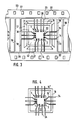
- the metal pattern includes a pair of first connector layers 20 extending on the main frame portion of the tape in the lengthwise direction of the tape and on the both sides of the tape, pairs of second connector layers 18 each running in the widthwise direction of the tape on the opposite sides of each hole 43 and connected to the pair of the first connector layers at their two ends, and third conductor layers 19 each running between the adjacent pairs of the second conductor layers 18 in parallel therewith and connected to the pair of the first conductor layers 20, a plurality of groups of leads 14 of 40 to 300 ⁇ m width each extending from the first and second connector layers 20 and 18 into the hole 43, crossing the four slits 17 and four strips 16 and fixed to the four strips 16.
- Plating process is conducted to the metal pattern by use of the first to third conductor layers 20, 18 and 19 as paths of plating current. Thereafter, a semiconductor element 1 having a plurality of bonding pads 2, that is, bump terminals is installed in the hole 43. Then, one ends 22 of the group of leads 14 are simultaneously bonded to respective bonding pads 2 of the semiconductor element 1 by gang bonding technique. Next, without any electrical test, the leads 14 and the strips 16 are cut at the slots 17 and along the dotted line 21, respectively, away from the main frame portion of the polyimide tape. At this time, the other ends 23 of the leads 14 are kept connected to the first and second connector layers 20 and 18. After the cutting process mentioned above, a structure shown in Fig. 4 is obtained. More particularly, the shortened leads 14' bonded at their one ends 22 to the bonding pads 2 of the semiconductor element 1 are attached to the suspending ring 16 of the tape and their other ends 24 are protruded from the suspending ring 16.
- the testing substrate 100 comprises a insulator body 60 and a metal pattern on the insulator body.
- the insulator body may be made of ceramic such as alumina (Al2O3) or resin material and have a thickness of 1 mm or more. Therefore, the substrate 100 is hardly deformed in the high temperature environment.
- a device setting portion 67 is provided which is a square or rectangular hole or recess 67 to accommodate the semiconductor element to be tested.
- Two small circular holes 68 are further provided for setting the test substrate 100 at a predetermined position and for transferring the test substrate. As shown in Fig.
- the upper surface of the body 60 at the periphery of the device setting portion 67 has the metal pattern including a plurality of terminals 62 of 200 to 500 ⁇ m width(W), a plurality of test pads 63 each having a size of 0.8 mm x 0.8 mm to 1.0 mm x 1.0 mm square and connected to each terminal 62 through a connecting path 64.
- the size of the test pad 63 on the insulator body 60 may be smaller than that of the test pad 36 on the prior art polyimide tape 31 shown in Fig. 1, because the insulator body of the testing substrate 100 is hardly deformed as mentioned above. Therefore, a larger number of test pads can be provided.
- the terminal 62, connecting path 64 and test pad 63 are continuously formed by metallized pattern on the ceramic body or by metal foil pattern on the resin body.
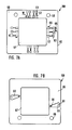
- Some terminals and test pads to which power sources such as Vcc, Vss or ground voltage are applied have small through-holes 65 and 66 as shown in Fig. 7A, through which a metallized area 69 formed on the back surface of the insulator body 60 as shown in Fig. 7B is electrically connected.
- the holes 65, 66 are filled with conductive material (not shown), and therefore the test pad 63 and the terminal 62 are connected to the metallic member 69 to remarkably reduce the electrical resistance between the test pad 63 and the terminal 62 even if the distance therebetween is large.
- the semiconductor element 1 is installed in the device setting portion 67 of the testing substrate 100, and the leads 14 are connected to the terminals 62 by solder 71 at their ends 24, respectively. Then, electrical tests including the bias test are conducted by contacting test probes or test electrodes 70 of a test apparatus (not shown) to the respective test pads 63 on the insulator body 60 of the testing substrate 100. After the electrical tests, the structure shown in Fig. 5A is delivered to a customer. The customer may perform the electrical tests again, and cuts the leads 14' at desired position between the semiconductor element 1 and the edge of the device setting portion 67 to obtain a semiconductor device, as shown in Fig.
- the semiconductor device shown in Fig. 6 can be installed on a circuit board as shown in Fig. 2, on a ceramic package, or on a lead frame.
- FIG. 8 in which the same components as those in Figs. 1 to 5 are indicated by the same reference numerals, another embodiment, where leads 84 are long, has a plastic tape 81 provided with double suspending strips 85 and 86 and double slots 87 and 88 in a hole 83. After, separation from the film carrier tape, the holdability of the leads can be improved. Further in this case, the inner suspending strip 85 can be left with the leads and the semiconductor device can be installed on the circuit board or the like with the inner suspending strip 85. Referring to Fig. 9, a larger number of test pads 63 can be provided by arranging them in two or more columns. In Fig. 9, the same components as those in Figs.
- 5A, 5B, 7A, 7B are indicated by the same reference numerals.
- longer connecting paths 64' has high electrical resistances. Therefore, corresponding test pad and terminal are connected by the metallic layer 69 on the back face via the through holes 65, 66 as described above with reference to Figs. 7A and 7B.
- a larger number of test pads can be provided without unfavorable enhancement of the electrical resistance.
Landscapes
- Testing Or Measuring Of Semiconductors Or The Like (AREA)
- Wire Bonding (AREA)
Applications Claiming Priority (4)
| Application Number | Priority Date | Filing Date | Title |
|---|---|---|---|
| JP60186061A JPH0740576B2 (ja) | 1985-08-23 | 1985-08-23 | フィルムキャリヤ半導体装置の電気試験方法 |
| JP186061/85 | 1985-08-23 | ||
| JP288786/85 | 1985-12-20 | ||
| JP60288786A JPH0740580B2 (ja) | 1985-12-20 | 1985-12-20 | 半導体素子の選別用基板および半導体素子の選別方法 |
Publications (3)
| Publication Number | Publication Date |
|---|---|
| EP0213575A2 true EP0213575A2 (fr) | 1987-03-11 |
| EP0213575A3 EP0213575A3 (en) | 1987-11-25 |
| EP0213575B1 EP0213575B1 (fr) | 1992-10-21 |
Family
ID=26503511
Family Applications (1)
| Application Number | Title | Priority Date | Filing Date |
|---|---|---|---|
| EP86111650A Expired - Lifetime EP0213575B1 (fr) | 1985-08-23 | 1986-08-22 | Procédé de fabrication d'un dispositif semi-conducteur utilisant une bande de support à film |
Country Status (3)
| Country | Link |
|---|---|
| US (1) | US4763409A (fr) |
| EP (1) | EP0213575B1 (fr) |
| DE (1) | DE3686990T2 (fr) |
Cited By (6)
| Publication number | Priority date | Publication date | Assignee | Title |
|---|---|---|---|---|
| EP0287451A1 (fr) * | 1987-04-17 | 1988-10-19 | Thomson-Csf | Procédé de connexion d'un composant électronique pour son test et son montage |
| EP0299768A3 (fr) * | 1987-07-14 | 1989-09-06 | Sharp Kabushiki Kaisha | Bande de support pour puces semi-conductrices |
| DE3809005A1 (de) * | 1988-03-17 | 1989-09-28 | Hitachi Semiconductor Europ Gm | Chipmodul und seine herstellung und verwendung |
| EP0406373A4 (en) * | 1988-12-07 | 1992-04-29 | Tribotech | Tape automated bonded lead package and reusable transport tape for use therewith |
| US5766983A (en) * | 1994-04-29 | 1998-06-16 | Hewlett-Packard Company | Tape automated bonding circuit with interior sprocket holes |
| RU2133522C1 (ru) * | 1997-11-03 | 1999-07-20 | Закрытое акционерное общество "Техно-ТМ" | Способ изготовления и контроля электронных компонентов |
Families Citing this family (34)
| Publication number | Priority date | Publication date | Assignee | Title |
|---|---|---|---|---|
| JPS63142894A (ja) * | 1986-12-06 | 1988-06-15 | 株式会社東芝 | フラツトパツケ−ジ集積回路の配線基板 |
| JPH0783036B2 (ja) * | 1987-12-11 | 1995-09-06 | 三菱電機株式会社 | キヤリアテープ |
| FR2625067A1 (fr) * | 1987-12-22 | 1989-06-23 | Sgs Thomson Microelectronics | Procede pour fixer sur un support un composant electronique et ses contacts |
| US4980219A (en) * | 1988-04-06 | 1990-12-25 | Casio Computer Co., Ltd. | Carrier tape for bonding IC devices and method of using the same |
| US4862827A (en) * | 1988-06-28 | 1989-09-05 | Wacker-Chemie Gmbh | Apparatus for coating semiconductor components on a dielectric film |
| US5121053A (en) * | 1988-10-11 | 1992-06-09 | Hewlett-Packard Company | Tab frame and process of testing same |
| US5184207A (en) * | 1988-12-07 | 1993-02-02 | Tribotech | Semiconductor die packages having lead support frame |
| USRE35578E (en) * | 1988-12-12 | 1997-08-12 | Sgs-Thomson Microelectronics, Inc. | Method to install an electronic component and its electrical connections on a support, and product obtained thereby |
| USRE35385E (en) * | 1988-12-12 | 1996-12-03 | Sgs-Thomson Microelectronics, Sa. | Method for fixing an electronic component and its contacts to a support |
| US4956605A (en) * | 1989-07-18 | 1990-09-11 | International Business Machines Corporation | Tab mounted chip burn-in apparatus |
| US5156983A (en) * | 1989-10-26 | 1992-10-20 | Digtial Equipment Corporation | Method of manufacturing tape automated bonding semiconductor package |
| US5008615A (en) * | 1989-11-03 | 1991-04-16 | Motorola, Inc. | Means and method for testing integrated circuits attached to a leadframe |
| US4995551A (en) * | 1990-04-24 | 1991-02-26 | Microelectronics And Computer Technology Corporation | Bonding electrical leads to pads on electrical components |
| US5076485A (en) * | 1990-04-24 | 1991-12-31 | Microelectronics And Computer Technology Corporation | Bonding electrical leads to pads with particles |
| US5029386A (en) * | 1990-09-17 | 1991-07-09 | Hewlett-Packard Company | Hierarchical tape automated bonding method |
| US5148003A (en) * | 1990-11-28 | 1992-09-15 | International Business Machines Corporation | Modular test oven |
| US5678301A (en) * | 1991-06-04 | 1997-10-21 | Micron Technology, Inc. | Method for forming an interconnect for testing unpackaged semiconductor dice |
| US5133118A (en) * | 1991-08-06 | 1992-07-28 | Sheldahl, Inc. | Surface mounted components on flex circuits |
| US5330919A (en) * | 1993-02-08 | 1994-07-19 | Motorola, Inc. | Method for electrically testing a semiconductor die using a test apparatus having an independent conductive plane |
| JPH06331678A (ja) * | 1993-05-13 | 1994-12-02 | Internatl Business Mach Corp <Ibm> | 電子部品のリード接続を検査する方法および装置 |
| JP2500785B2 (ja) * | 1993-09-20 | 1996-05-29 | 日本電気株式会社 | 半導体パッケ―ジ用フィルムキャリアテ−プ及びこれを用いた半導体装置 |
| US5367763A (en) * | 1993-09-30 | 1994-11-29 | Atmel Corporation | TAB testing of area array interconnected chips |
| US5920114A (en) | 1997-09-25 | 1999-07-06 | International Business Machines Corporation | Leadframe having resilient carrier positioning means |
| US6274405B1 (en) * | 1996-10-17 | 2001-08-14 | Seiko Epson Corporation | Semiconductor device, method of making the same, circuit board, and film carrier tape |
| KR100205353B1 (ko) * | 1996-12-27 | 1999-07-01 | 구본준 | 프리-몰드 패들을 갖는 반도체 패키지 제조 공정용 리드 프레임 |
| JP3022819B2 (ja) * | 1997-08-27 | 2000-03-21 | 日本電気アイシーマイコンシステム株式会社 | 半導体集積回路装置 |
| US6473702B1 (en) * | 2000-06-27 | 2002-10-29 | Advanced Micro Devices, Inc. | System and method for integrated singulation and inspection of semiconductor devices |
| JP3675364B2 (ja) * | 2001-05-30 | 2005-07-27 | ソニー株式会社 | 半導体装置用基板その製造方法および半導体装置 |
| US6783316B2 (en) * | 2001-06-26 | 2004-08-31 | Asm Assembly Automation Limited | Apparatus and method for testing semiconductor devices |
| DE10213296B9 (de) * | 2002-03-25 | 2007-04-19 | Infineon Technologies Ag | Elektronisches Bauteil mit einem Halbleiterchip, Verfahren zu seiner Herstellung und Verfahren zur Herstellung eines Nutzens |
| US7271047B1 (en) * | 2006-01-06 | 2007-09-18 | Advanced Micro Devices, Inc. | Test structure and method for measuring the resistance of line-end vias |
| US20110012240A1 (en) * | 2009-07-15 | 2011-01-20 | Chenglin Liu | Multi-Connect Lead |
| CN107770956A (zh) * | 2016-08-16 | 2018-03-06 | 光宝电子(广州)有限公司 | 电路板结构 |
| US11908705B2 (en) * | 2021-10-18 | 2024-02-20 | Texas Instruments Incorporated | Interconnect singulation |
Family Cites Families (13)
| Publication number | Priority date | Publication date | Assignee | Title |
|---|---|---|---|---|
| US2795043A (en) * | 1954-08-16 | 1957-06-11 | Fleischer Ruth | Device for administering medicine to be attached to a spoon handle |
| DE1909480C2 (de) * | 1968-03-01 | 1984-10-11 | General Electric Co., Schenectady, N.Y. | Trägeranordnung und Verfahren zur elektrischen Kontaktierung von Halbleiterchips |
| US3678385A (en) * | 1969-09-26 | 1972-07-18 | Amp Inc | Assembly and test device for microelectronic circuit members |
| JPS517096B1 (fr) * | 1971-03-10 | 1976-03-04 | ||
| US3777365A (en) * | 1972-03-06 | 1973-12-11 | Honeywell Inf Systems | Circuit chips having beam leads attached by film strip process |
| US4026008A (en) * | 1972-10-02 | 1977-05-31 | Signetics Corporation | Semiconductor lead structure and assembly and method for fabricating same |
| US3859718A (en) * | 1973-01-02 | 1975-01-14 | Texas Instruments Inc | Method and apparatus for the assembly of semiconductor devices |
| US3838984A (en) * | 1973-04-16 | 1974-10-01 | Sperry Rand Corp | Flexible carrier and interconnect for uncased ic chips |
| CA1052912A (fr) * | 1975-07-07 | 1979-04-17 | National Semiconductor Corporation | Mode de fabrication d'un ruban d'interconnexion pour le groupage de dispositifs a semiconducteur |
| US4138691A (en) * | 1977-06-07 | 1979-02-06 | Nippon Electric Co., Ltd. | Framed lead assembly for a semiconductor device comprising insulator reinforcing strips supported by a frame and made integral with lead strips |
| JPS5826828B2 (ja) * | 1978-04-26 | 1983-06-06 | 新光電気工業株式会社 | テ−プキヤリアの製造方法 |
| US4411719A (en) * | 1980-02-07 | 1983-10-25 | Westinghouse Electric Corp. | Apparatus and method for tape bonding and testing of integrated circuit chips |
| US4308339A (en) * | 1980-02-07 | 1981-12-29 | Westinghouse Electric Corp. | Method for manufacturing tape including lead frames |
-
1986
- 1986-08-22 EP EP86111650A patent/EP0213575B1/fr not_active Expired - Lifetime
- 1986-08-22 DE DE8686111650T patent/DE3686990T2/de not_active Expired - Fee Related
- 1986-08-25 US US06/899,896 patent/US4763409A/en not_active Expired - Lifetime
Cited By (7)
| Publication number | Priority date | Publication date | Assignee | Title |
|---|---|---|---|---|
| EP0287451A1 (fr) * | 1987-04-17 | 1988-10-19 | Thomson-Csf | Procédé de connexion d'un composant électronique pour son test et son montage |
| FR2614134A1 (fr) * | 1987-04-17 | 1988-10-21 | Cimsa Sintra | Procede de connexion d'un composant electronique pour son test et son montage, et dispositif de mise en oeuvre de ce procede |
| EP0299768A3 (fr) * | 1987-07-14 | 1989-09-06 | Sharp Kabushiki Kaisha | Bande de support pour puces semi-conductrices |
| DE3809005A1 (de) * | 1988-03-17 | 1989-09-28 | Hitachi Semiconductor Europ Gm | Chipmodul und seine herstellung und verwendung |
| EP0406373A4 (en) * | 1988-12-07 | 1992-04-29 | Tribotech | Tape automated bonded lead package and reusable transport tape for use therewith |
| US5766983A (en) * | 1994-04-29 | 1998-06-16 | Hewlett-Packard Company | Tape automated bonding circuit with interior sprocket holes |
| RU2133522C1 (ru) * | 1997-11-03 | 1999-07-20 | Закрытое акционерное общество "Техно-ТМ" | Способ изготовления и контроля электронных компонентов |
Also Published As
| Publication number | Publication date |
|---|---|
| US4763409A (en) | 1988-08-16 |
| DE3686990D1 (de) | 1992-11-26 |
| DE3686990T2 (de) | 1993-04-22 |
| EP0213575B1 (fr) | 1992-10-21 |
| EP0213575A3 (en) | 1987-11-25 |
Similar Documents
| Publication | Publication Date | Title |
|---|---|---|
| US4763409A (en) | Method of manufacturing semiconductor device | |
| US4750089A (en) | Circuit board with a chip carrier and mounting structure connected to the chip carrier | |
| EP0120500B1 (fr) | Empaquetage pour LSI à haute densité pour circuits logiques | |
| EP0073149B1 (fr) | Module de montage pour puce semi-conductrice | |
| US6028358A (en) | Package for a semiconductor device and a semiconductor device | |
| US4647959A (en) | Integrated circuit package, and method of forming an integrated circuit package | |
| US4812949A (en) | Method of and apparatus for mounting an IC chip | |
| EP0856889B1 (fr) | Structure de montage d'un dispositif semiconducteur et procédé pour le montage d'un dispositif semiconducteur | |
| US4890194A (en) | A chip carrier and mounting structure connected to the chip carrier | |
| US4792532A (en) | Semiconductor device and process for producing the same, and tape carrier used in said process | |
| US5357400A (en) | Tape automated bonding semiconductor device and production process thereof | |
| EP0683517A2 (fr) | Dispositif semi-conducteur ayant une puce semi-conductrice connectée avec une plaque de circuit par des plots de contact et procédé de montage | |
| US6255833B1 (en) | Method for testing semiconductor dice and chip scale packages | |
| JPH0332914B2 (fr) | ||
| JPH0767002B2 (ja) | 回路パッケージ構造 | |
| EP0314707A1 (fr) | Liaisons par fils et contacts electriques d'un dispositif a circuit integre. | |
| JPH05205832A (ja) | フレキシブルテープ構造及びフレキシブルテープ形成プロセス | |
| US5355105A (en) | Multi-layer flexible printed circuit and method of making same | |
| JPH11176885A (ja) | 半導体装置及びその製造方法、フィルムキャリアテープ、回路基板並びに電子機器 | |
| EP0186818B1 (fr) | Procédé de connexion de broches à des plaquettes semiconductrices | |
| JP2025501976A (ja) | 絶縁を有する半導体デバイスパッケージを製造するための方法 | |
| US6639416B1 (en) | Method and apparatus for testing semiconductor dice | |
| JP2001007252A (ja) | 半導体装置およびその製造方法 | |
| JPS6246537A (ja) | フィルムキャリヤ半導体装置の電気試験方法 | |
| US6410937B1 (en) | Integrated circuit chip carrier |
Legal Events
| Date | Code | Title | Description |
|---|---|---|---|
| PUAI | Public reference made under article 153(3) epc to a published international application that has entered the european phase |
Free format text: ORIGINAL CODE: 0009012 |
|
| 17P | Request for examination filed |
Effective date: 19860822 |
|
| AK | Designated contracting states |
Kind code of ref document: A2 Designated state(s): DE FR GB |
|
| PUAL | Search report despatched |
Free format text: ORIGINAL CODE: 0009013 |
|
| AK | Designated contracting states |
Kind code of ref document: A3 Designated state(s): DE FR GB |
|
| 17Q | First examination report despatched |
Effective date: 19900618 |
|
| GRAA | (expected) grant |
Free format text: ORIGINAL CODE: 0009210 |
|
| AK | Designated contracting states |
Kind code of ref document: B1 Designated state(s): DE FR GB |
|
| RIN1 | Information on inventor provided before grant (corrected) |
Inventor name: BONKOHARA, MANABU Inventor name: TAKEKAWA, KOUICHI |
|
| REF | Corresponds to: |
Ref document number: 3686990 Country of ref document: DE Date of ref document: 19921126 |
|
| ET | Fr: translation filed | ||
| PLBE | No opposition filed within time limit |
Free format text: ORIGINAL CODE: 0009261 |
|
| STAA | Information on the status of an ep patent application or granted ep patent |
Free format text: STATUS: NO OPPOSITION FILED WITHIN TIME LIMIT |
|
| 26N | No opposition filed | ||
| PGFP | Annual fee paid to national office [announced via postgrant information from national office to epo] |
Ref country code: GB Payment date: 19940816 Year of fee payment: 9 |
|
| PG25 | Lapsed in a contracting state [announced via postgrant information from national office to epo] |
Ref country code: GB Effective date: 19950822 |
|
| GBPC | Gb: european patent ceased through non-payment of renewal fee |
Effective date: 19950822 |
|
| PGFP | Annual fee paid to national office [announced via postgrant information from national office to epo] |
Ref country code: FR Payment date: 20000811 Year of fee payment: 15 |
|
| PGFP | Annual fee paid to national office [announced via postgrant information from national office to epo] |
Ref country code: DE Payment date: 20000814 Year of fee payment: 15 |
|
| PG25 | Lapsed in a contracting state [announced via postgrant information from national office to epo] |
Ref country code: FR Free format text: LAPSE BECAUSE OF NON-PAYMENT OF DUE FEES Effective date: 20020430 |
|
| PG25 | Lapsed in a contracting state [announced via postgrant information from national office to epo] |
Ref country code: DE Free format text: LAPSE BECAUSE OF NON-PAYMENT OF DUE FEES Effective date: 20020501 |
|
| REG | Reference to a national code |
Ref country code: FR Ref legal event code: ST |