EP0213920A2 - Méthode pour dessiner un motif sur une pastille à l'aide d'un faisceau de particules chargées - Google Patents
Méthode pour dessiner un motif sur une pastille à l'aide d'un faisceau de particules chargées Download PDFInfo
- Publication number
- EP0213920A2 EP0213920A2 EP86306579A EP86306579A EP0213920A2 EP 0213920 A2 EP0213920 A2 EP 0213920A2 EP 86306579 A EP86306579 A EP 86306579A EP 86306579 A EP86306579 A EP 86306579A EP 0213920 A2 EP0213920 A2 EP 0213920A2
- Authority
- EP
- European Patent Office
- Prior art keywords
- pattern
- subfield
- data
- width
- region
- Prior art date
- Legal status (The legal status is an assumption and is not a legal conclusion. Google has not performed a legal analysis and makes no representation as to the accuracy of the status listed.)
- Granted
Links
Images



Classifications
-
- H—ELECTRICITY
- H10—SEMICONDUCTOR DEVICES; ELECTRIC SOLID-STATE DEVICES NOT OTHERWISE PROVIDED FOR
- H10P—GENERIC PROCESSES OR APPARATUS FOR THE MANUFACTURE OR TREATMENT OF DEVICES COVERED BY CLASS H10
- H10P54/00—Cutting or separating of wafers, substrates or parts of devices
-
- H—ELECTRICITY
- H01—ELECTRIC ELEMENTS
- H01J—ELECTRIC DISCHARGE TUBES OR DISCHARGE LAMPS
- H01J37/00—Discharge tubes with provision for introducing objects or material to be exposed to the discharge, e.g. for the purpose of examination or processing thereof
- H01J37/30—Electron-beam or ion-beam tubes for localised treatment of objects
- H01J37/302—Controlling tubes by external information, e.g. program control
- H01J37/3023—Program control
- H01J37/3026—Patterning strategy
-
- G—PHYSICS
- G03—PHOTOGRAPHY; CINEMATOGRAPHY; ANALOGOUS TECHNIQUES USING WAVES OTHER THAN OPTICAL WAVES; ELECTROGRAPHY; HOLOGRAPHY
- G03F—PHOTOMECHANICAL PRODUCTION OF TEXTURED OR PATTERNED SURFACES, e.g. FOR PRINTING, FOR PROCESSING OF SEMICONDUCTOR DEVICES; MATERIALS THEREFOR; ORIGINALS THEREFOR; APPARATUS SPECIALLY ADAPTED THEREFOR
- G03F1/00—Originals for photomechanical production of textured or patterned surfaces, e.g., masks, photo-masks, reticles; Mask blanks or pellicles therefor; Containers specially adapted therefor; Preparation thereof
- G03F1/20—Masks or mask blanks for imaging by charged particle beam [CPB] radiation, e.g. by electron beam; Preparation thereof
-
- H—ELECTRICITY
- H10—SEMICONDUCTOR DEVICES; ELECTRIC SOLID-STATE DEVICES NOT OTHERWISE PROVIDED FOR
- H10P—GENERIC PROCESSES OR APPARATUS FOR THE MANUFACTURE OR TREATMENT OF DEVICES COVERED BY CLASS H10
- H10P76/00—Manufacture or treatment of masks on semiconductor bodies, e.g. by lithography or photolithography
Definitions
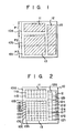
- LSI chip area l0 having an LSI pattern formed based on a CAD (Computer Aided Design) output is illustrated.
- CAD Computer Aided Design
- hatched regions ll to l3 are pattern regions.
- regions ll to l3 are pattern regions.
- patterns included in regions ll and l2 are not repeating type, but region l3 includes repeating type patterns such as memory cells.
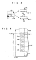
- subfield region l2c is divided into two portions which are included in frames l0a and l0b, respectively, and divided portions of subfield region l2f are included in frames l0b and l0c, respectively. Accordingly, a pattern in subfield region l2c may be undesirably separated into frames l0a and l0b.
- the main feature of the present invention is to minimize the number of divided drawing patterns of subfields at the boundary between adjacent frames, to prevent an increase in the number of data, and to improve the throughput and precision of drawing.
- repetition data (number of repetitive patterns and repetition pitch) corresponding to a repetition pattern represented by the pattern of memory element in Fig. ll, for example, is obtained by the operator.
- reference numeral 60 denotes an LSI chip area; 6l and 62, nonrepetitive regions; and 63, a repetitive region.
- An example of the data format of the repetition data is shown in Fig. l0.
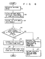
- frame data as a set of subfield groups in which a drawing start position of the subfield is included in the logical frame and an end position thereof is included in maximum physical frame width R is acquired for frame regions 60a to 60c.
- the data of the lower left corner point of chip pattern 60 supplied from computer 30 is given as (0,0), and the lower left corner point of pattern region 63 is given as (a,b). Accordingly, as shown in Fig. ll, when region 63 is divided into subfields 63e to 63h, 63i,..., the start point of subfield 63e is also given as (a,b). Similarly, start points of subfields 63f to 63i are respectively simply calculated by computer 30 using pitch data D to be (a,b+D), (a,b+2D), (a,b+3D), and (a,b+4D).
- a plurality of subfields at a lower portion of pattern region 62 are included in frame 60c.
- the same determination as for subfield 63h of Fig. ll is performed by computer 30 for subfield regions 62a and 63b, and it is determined whether pattern data of regions 62a and 62b is included in frame 60c.
- the lower left corner of chip 60 is given as origin (0,0).
- beam start positions corresponding to the respective subfield regions are given as lower left corner points (al,0) and (a2,0) of field regions 7l, 72,..., by main deflector 4l.
- main deflector 4l sets the start position of beam 46 at origin (0,0), and subdeflector 43 performs necessary pattern drawing in region 7l.
- the start position of beam 46 is then set at point (a3,0) representing the start position of subfield 74, and subdeflector 43 performs necessary pattern drawing in region 74.
- an LSI chip area is divided into subfields and then virtually divided into frames to constitute frame data as a group of subfield data including subfields in the frames. Therefore, an increase in throughput and an improvement in drawing precision can be achieved.
- the present invention will contribute to future LSI micropatterning and higher integration.
- an arrangement of the drawing apparatus with an electron beam is not limited to that of Fig. 5 but can be changed in accordance with specifications as needed.
- the apparatus can also be applied to a method of drawing with an ion beam instead of an electron beam.
- the width of subfield is not required to be set equal to that of subdeflection, and the width can be set less than that of the subdeflection.
- the main deflector of electromagnetic type is used in the embodiment, but an electrostatic type main deflector, such as electrostatic deflection plates or a deflector of eight poles can also be used.
Landscapes
- Chemical & Material Sciences (AREA)
- Analytical Chemistry (AREA)
- Physics & Mathematics (AREA)
- General Physics & Mathematics (AREA)
- Electron Beam Exposure (AREA)
Applications Claiming Priority (2)
| Application Number | Priority Date | Filing Date | Title |
|---|---|---|---|
| JP185530/85 | 1985-08-23 | ||
| JP60185530A JPS6246518A (ja) | 1985-08-23 | 1985-08-23 | 荷電ビ−ム描画方法 |
Publications (3)
| Publication Number | Publication Date |
|---|---|
| EP0213920A2 true EP0213920A2 (fr) | 1987-03-11 |
| EP0213920A3 EP0213920A3 (en) | 1989-01-18 |
| EP0213920B1 EP0213920B1 (fr) | 1990-10-24 |
Family
ID=16172412
Family Applications (1)
| Application Number | Title | Priority Date | Filing Date |
|---|---|---|---|
| EP86306579A Expired - Lifetime EP0213920B1 (fr) | 1985-08-23 | 1986-08-26 | Méthode pour dessiner un motif sur une pastille à l'aide d'un faisceau de particules chargées |
Country Status (5)
| Country | Link |
|---|---|
| US (1) | US4989156A (fr) |
| EP (1) | EP0213920B1 (fr) |
| JP (1) | JPS6246518A (fr) |
| KR (1) | KR900001983B1 (fr) |
| DE (1) | DE3675120D1 (fr) |
Families Citing this family (15)
| Publication number | Priority date | Publication date | Assignee | Title |
|---|---|---|---|---|
| US5309354A (en) * | 1991-10-30 | 1994-05-03 | International Business Machines Corporation | Electron beam exposure method |
| US5446649A (en) * | 1992-12-31 | 1995-08-29 | International Business Machines Corporation | Data-hiding and skew scan for unioning of shapes in electron beam lithography post-processing |
| JP3601630B2 (ja) * | 1995-11-01 | 2004-12-15 | 株式会社ニコン | 荷電粒子線転写方法 |
| US6091072A (en) * | 1997-10-23 | 2000-07-18 | International Business Machines Corporation | Piece-wise processing of very large semiconductor designs |
| JP4206192B2 (ja) * | 2000-11-09 | 2009-01-07 | 株式会社日立製作所 | パターン検査方法及び装置 |
| DE19911372A1 (de) * | 1999-03-15 | 2000-09-28 | Pms Gmbh | Vorrichtung zum Steuern eines Strahls aus elektrisch geladenen Teilchen |
| US6425113B1 (en) * | 2000-06-13 | 2002-07-23 | Leigh C. Anderson | Integrated verification and manufacturability tool |
| US7412676B2 (en) * | 2000-06-13 | 2008-08-12 | Nicolas B Cobb | Integrated OPC verification tool |
| US7861207B2 (en) | 2004-02-25 | 2010-12-28 | Mentor Graphics Corporation | Fragmentation point and simulation site adjustment for resolution enhancement techniques |
| US7234130B2 (en) * | 2004-02-25 | 2007-06-19 | James Word | Long range corrections in integrated circuit layout designs |
| US8037429B2 (en) * | 2005-03-02 | 2011-10-11 | Mentor Graphics Corporation | Model-based SRAF insertion |
| US7493587B2 (en) * | 2005-03-02 | 2009-02-17 | James Word | Chromeless phase shifting mask for integrated circuits using interior region |
| US7506285B2 (en) | 2006-02-17 | 2009-03-17 | Mohamed Al-Imam | Multi-dimensional analysis for predicting RET model accuracy |
| JP2008010547A (ja) * | 2006-06-28 | 2008-01-17 | Elpida Memory Inc | 電子線描画方法、電子線描画装置、及び電子線描画プログラム |
| US7799487B2 (en) * | 2007-02-09 | 2010-09-21 | Ayman Yehia Hamouda | Dual metric OPC |
Family Cites Families (9)
| Publication number | Priority date | Publication date | Assignee | Title |
|---|---|---|---|---|
| US4132898A (en) * | 1977-11-01 | 1979-01-02 | Fujitsu Limited | Overlapping boundary electron exposure system method and apparatus |
| DE3169257D1 (en) * | 1980-11-28 | 1985-04-18 | Ibm | Electron beam system and method |
| US4430571A (en) * | 1981-04-16 | 1984-02-07 | Control Data Corporation | Method and apparatus for exposing multi-level registered patterns interchangeably between stations of a multi-station electron-beam array lithography (EBAL) system |
| JPS57204125A (en) * | 1981-06-10 | 1982-12-14 | Hitachi Ltd | Electron-ray drawing device |
| DD203429A1 (de) * | 1981-08-03 | 1983-10-19 | Eichhorn Hans Guenther | Schaltungsanordnung zur steuerung eines korpuskularstrahls |
| JPS5957431A (ja) * | 1982-09-27 | 1984-04-03 | Fujitsu Ltd | 電子ビ−ム露光装置 |
| JPS59114818A (ja) * | 1982-12-21 | 1984-07-03 | Toshiba Corp | 電子ビ−ムパタ−ン描画方法 |
| US4692579A (en) * | 1984-05-18 | 1987-09-08 | Hitachi, Ltd. | Electron beam lithography apparatus |
| US4628466A (en) * | 1984-10-29 | 1986-12-09 | Excellon Industries | Method and apparatus for pattern forming |
-
1985
- 1985-08-23 JP JP60185530A patent/JPS6246518A/ja active Granted
-
1986
- 1986-08-22 KR KR1019860006966A patent/KR900001983B1/ko not_active Expired
- 1986-08-26 DE DE8686306579T patent/DE3675120D1/de not_active Expired - Lifetime
- 1986-08-26 EP EP86306579A patent/EP0213920B1/fr not_active Expired - Lifetime
-
1990
- 1990-05-16 US US07/523,829 patent/US4989156A/en not_active Expired - Lifetime
Also Published As
| Publication number | Publication date |
|---|---|
| JPH0357608B2 (fr) | 1991-09-02 |
| KR870002639A (ko) | 1987-04-06 |
| US4989156A (en) | 1991-01-29 |
| KR900001983B1 (ko) | 1990-03-30 |
| EP0213920A3 (en) | 1989-01-18 |
| DE3675120D1 (de) | 1990-11-29 |
| JPS6246518A (ja) | 1987-02-28 |
| EP0213920B1 (fr) | 1990-10-24 |
Similar Documents
| Publication | Publication Date | Title |
|---|---|---|
| EP0213920A2 (fr) | Méthode pour dessiner un motif sur une pastille à l'aide d'un faisceau de particules chargées | |
| JPS63199421A (ja) | 荷電ビ−ム描画方法 | |
| JP4054445B2 (ja) | 荷電ビーム描画方法 | |
| JP2786676B2 (ja) | 荷電ビーム描画方法 | |
| JP3454974B2 (ja) | 荷電ビーム描画方法 | |
| JP3964606B2 (ja) | 荷電ビーム描画装置、荷電ビーム描画方法、およびコンピュータ読み取り可能な記録媒体 | |
| JPH0574693A (ja) | 荷電ビーム描画方法 | |
| JP2894746B2 (ja) | 荷電ビーム描画方法 | |
| JP3274149B2 (ja) | 荷電ビーム描画方法 | |
| JP3319519B2 (ja) | 荷電ビーム描画方法 | |
| JP3004034B2 (ja) | 荷電ビーム描画方法 | |
| JP2664746B2 (ja) | 電荷ビーム描画方法 | |
| JP2839587B2 (ja) | 荷電ビーム描画方法 | |
| JP2664732B2 (ja) | 荷電ビーム描画方法 | |
| JPH025406A (ja) | 荷電ビーム描画方法 | |
| JPH01152726A (ja) | 荷電ビーム描画方法 | |
| JP3462074B2 (ja) | 描画データ作成方法 | |
| JP2786671B2 (ja) | 荷電ビーム描画方法 | |
| JPH0697058A (ja) | 電子ビーム描画装置用の描画データ作成方法 | |
| JPS63127532A (ja) | 荷電ビ−ム描画方法 | |
| JPS6272124A (ja) | 荷電粒子ビ−ム描画方法 | |
| JPH01243520A (ja) | 荷電ビーム描画方法 | |
| JPH03150836A (ja) | 荷電ビーム描画方法 | |
| KR19980070537A (ko) | 전자선 묘화용 eb 마스크 제조 방법 및 eb 마스크 제조 장치 | |
| JPH04302413A (ja) | 荷電ビーム描画装置 |
Legal Events
| Date | Code | Title | Description |
|---|---|---|---|
| PUAI | Public reference made under article 153(3) epc to a published international application that has entered the european phase |
Free format text: ORIGINAL CODE: 0009012 |
|
| AK | Designated contracting states |
Kind code of ref document: A2 Designated state(s): DE FR GB |
|
| 17P | Request for examination filed |
Effective date: 19880208 |
|
| PUAL | Search report despatched |
Free format text: ORIGINAL CODE: 0009013 |
|
| AK | Designated contracting states |
Kind code of ref document: A3 Designated state(s): DE FR GB |
|
| 17Q | First examination report despatched |
Effective date: 19890609 |
|
| GRAA | (expected) grant |
Free format text: ORIGINAL CODE: 0009210 |
|
| AK | Designated contracting states |
Kind code of ref document: B1 Designated state(s): DE FR GB |
|
| REF | Corresponds to: |
Ref document number: 3675120 Country of ref document: DE Date of ref document: 19901129 |
|
| ET | Fr: translation filed | ||
| PLBE | No opposition filed within time limit |
Free format text: ORIGINAL CODE: 0009261 |
|
| STAA | Information on the status of an ep patent application or granted ep patent |
Free format text: STATUS: NO OPPOSITION FILED WITHIN TIME LIMIT |
|
| 26N | No opposition filed | ||
| REG | Reference to a national code |
Ref country code: GB Ref legal event code: 746 Effective date: 19981026 |
|
| REG | Reference to a national code |
Ref country code: FR Ref legal event code: D6 |
|
| REG | Reference to a national code |
Ref country code: GB Ref legal event code: IF02 |
|
| PGFP | Annual fee paid to national office [announced via postgrant information from national office to epo] |
Ref country code: FR Payment date: 20050809 Year of fee payment: 20 |
|
| PGFP | Annual fee paid to national office [announced via postgrant information from national office to epo] |
Ref country code: DE Payment date: 20050818 Year of fee payment: 20 |
|
| PGFP | Annual fee paid to national office [announced via postgrant information from national office to epo] |
Ref country code: GB Payment date: 20050824 Year of fee payment: 20 |
|
| PG25 | Lapsed in a contracting state [announced via postgrant information from national office to epo] |
Ref country code: GB Free format text: LAPSE BECAUSE OF EXPIRATION OF PROTECTION Effective date: 20060825 |
|
| REG | Reference to a national code |
Ref country code: GB Ref legal event code: PE20 |