EP0214621B1 - Packung mit einem Substrat und mindestens einem elektronischen Bauelement - Google Patents
Packung mit einem Substrat und mindestens einem elektronischen Bauelement Download PDFInfo
- Publication number
- EP0214621B1 EP0214621B1 EP86112244A EP86112244A EP0214621B1 EP 0214621 B1 EP0214621 B1 EP 0214621B1 EP 86112244 A EP86112244 A EP 86112244A EP 86112244 A EP86112244 A EP 86112244A EP 0214621 B1 EP0214621 B1 EP 0214621B1
- Authority
- EP
- European Patent Office
- Prior art keywords
- substrate
- silicone material
- package
- silicone
- leads
- Prior art date
- Legal status (The legal status is an assumption and is not a legal conclusion. Google has not performed a legal analysis and makes no representation as to the accuracy of the status listed.)
- Expired - Lifetime
Links
Images

Classifications
-
- H—ELECTRICITY
- H10—SEMICONDUCTOR DEVICES; ELECTRIC SOLID-STATE DEVICES NOT OTHERWISE PROVIDED FOR
- H10W—GENERIC PACKAGES, INTERCONNECTIONS, CONNECTORS OR OTHER CONSTRUCTIONAL DETAILS OF DEVICES COVERED BY CLASS H10
- H10W76/00—Containers; Fillings or auxiliary members therefor; Seals
- H10W76/40—Fillings or auxiliary members in containers, e.g. centering rings
- H10W76/42—Fillings
- H10W76/47—Solid or gel fillings
-
- H—ELECTRICITY
- H10—SEMICONDUCTOR DEVICES; ELECTRIC SOLID-STATE DEVICES NOT OTHERWISE PROVIDED FOR
- H10W—GENERIC PACKAGES, INTERCONNECTIONS, CONNECTORS OR OTHER CONSTRUCTIONAL DETAILS OF DEVICES COVERED BY CLASS H10
- H10W76/00—Containers; Fillings or auxiliary members therefor; Seals
- H10W76/10—Containers or parts thereof
- H10W76/12—Containers or parts thereof characterised by their shape
-
- H—ELECTRICITY
- H10—SEMICONDUCTOR DEVICES; ELECTRIC SOLID-STATE DEVICES NOT OTHERWISE PROVIDED FOR
- H10W—GENERIC PACKAGES, INTERCONNECTIONS, CONNECTORS OR OTHER CONSTRUCTIONAL DETAILS OF DEVICES COVERED BY CLASS H10
- H10W90/00—Package configurations
Definitions
- the present invention relates to a package with electronic components mounted to be easily removed without damage.
- IC integrated circuit
- US-A-4 326 238 discloses an electronic circuit package in which an electronic circuit element together with connecting beam leads is embedded in resin layers.
- the resin layers are cured by air oxidation which starts from the surface of the resin, thereby enabling, for a certain period of time, the easy replacement of the electronic element (e.g. after product testing).
- One object of the invention is, therefore, to provide a package free from the above-mentioned disadvantages in the conventional package.
- a package which comprises: a substrate; a plurality of pads formed on the upper surface of said substrate; at least one electronic component having a plurality of leads to be connected to said pads and mounted on the upper surface of said substrate; a fluid silicone material provided on the upper surface of said substrate to fill the space beneath said leads and the lower surface of said electronic component or even to completely embed said leads; and a gel-state silicone material which covers the fluid silicone material and the remaining upper surface, if any of said substrate.
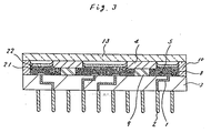
- a first embodiment of the invention comprises a substrate 3 including a plurality of conductive wirings 1; a plurality of input/output pins 2 provided on the lower surface of the substrate 3; a plurality of pads 8 provided on the upper surface of the substrate 3; a frame 10 made of iron-nickel-cobalt alloy and fitted onto the circumference of the upper surface of the substrate 3 with an adhesive (for instance, an epoxy adhesive); a cap 13 made of aluminum nitride and so fitted to the frame 10 with an adhesive as to be opposite to the upper surface of the substrate 3; a plurality of spacers 9 made of silicone rubber and fixed to the upper surface of the substrate 3 with an adhesive; a plurality of integrated circuit (IC) chips 4 fixed to the spacers 9 with an adhesive; and first silicone-filled portions 11 and a second silicone-filled portion 12 formed by a method, which will be described later on.
- IC integrated circuit
- the cap 13 Onto the upper surface of the cap 13 may be fitted one or more heat sinks for air-cooling or water-cooling. Between the lower surface of the cap 13 and the upper surfaces of the chips 4 may be inserted a compound having a good heat-conductivity. Heat generating from the chips 4 is transmitted either directly or through the compound to the cap 13, and further dispersed outside through the heat sink. If the frame 10 is formed of an electrically insulating material, an electro-conductive adhesive can be used.
- each of the chips 4 are fitted one ends of a plurality of leads 5 at minute intervals.
- the other ends of the leads 5, radially extending from the chips 4, are connected to the pads 8 by bonding.
- the pins 2 and circuits contained within the chips 4 are electrically connected through the wirings 1, the pads 8 and the leads 5.
- a first fluid silicone material having a high viscousness is filled by using an injector into spaces 11a, which are formed below the chips 4.
- Each of the spaces 11a is surrounded by the lower surface of the corresponding one of the chips 4, the corresponding ones of the leads 5, four sides of the corresponding one of the spacers 9 and the upper surface of the substrate 3.
- the first silicone-filled portions 11 are formed.
- this first silicone material for instance, silicone impregnant available from Shinetsu Silicone Company under the trade name KJF-812 may be used.
- KJF-812 silicone impregnant available from Shinetsu Silicone Company under the trade name KJF-812
- the second silicone material for instance, heat-hardened type potting agent available from Toray Silicone Company, Ltd. under the trade name SH1851 may be used. Since the first silicone material has a higher viscousness than the second silicone material, the former remains within the spaces 11a not to mix with the latter. After that, the entire package is kept for an hour or two in an air atmosphere at about 125°C (degrees centigrade) to harden the second silicone material into a gel state. At this time, the first silicone material does not become hard. The portions 11 and 12 thus formed protect wirings formed on the upper surface of the substrate 3 from moisture and other undesirable factors.
- the first silicone material used in the embodiment has a high viscousness
- other fluid silicone materials having a lower viscousness may be used as well.
- the substrate 3 is turned upside down after pouring such a fluid silicone material over the substrate 3.
- the fluid silicone material within the spaces 11a remains as it stands due to its surface tension.
- the second silicone material is poured and it alone is hardened by heating.
- an ultraviolet (UV) hardened type silicone material can be used for both the portions 11 and 12.
- the UV-hardened type silicone material is poured over the substrate 3. An UV ray is then irradiated from above, so that the part of the poured silicone material hidden by the chips 4 and the leads 5 when the substrate 3 is viewed from above, is unhardened to constitute the portions 11 while the remaining part is hardened into a gel state to form the portion 12.
- TUV6000 the one available from Toshiba Silicone Company under the trade name TUV6000 may be used.
- the chips 4 and the frame 10 are first mounted over the substrate 3.
- a third silicone material is poured to form silicone-filled portions 21 of sufficient height to have the leads 5 embedded therein, followed by the pouring of a fourth silicone material for the forming of a fourth silicone-filled portion 22.
- the third and fourth silicone materials the above-mentioned KJF-812 and SH1851 may be employed, respectively.
- the entire package is then kept for an hour or two in an air atmosphere at about 125°C to harden the fourth silicone material alone into a gel state.
- the cap 13 is fitted to the frame 10 to complete the package.
- the heat-hardened type silicone material is used for the fourth silicone material in the embodiment
- an UV-hardened type one like TUV6000 mentioned above, may be used as well.
- the fourth silicone material is hardened by UV irradiation.
- the first through fourth silicone materials of the packages assembled as described above according to the invention are to be removed from the portions 11, 12, 21 and 22 to replace the chips or for any other purpose in changing the design of or repairing the package, the first or third silicone material can be readily washed away from the portion 11 or 21 with organic solvent after removing the second or fourth silicone material from the portion 12 or 22. Therefore, in neither the first nor the second embodiment, the leads 5 will be cut or come off the pads 8 in the process of the silicone removal.
Landscapes
- Structures Or Materials For Encapsulating Or Coating Semiconductor Devices Or Solid State Devices (AREA)
- Cooling Or The Like Of Semiconductors Or Solid State Devices (AREA)
Claims (5)
- Packung mit:
einem Substrat (3);
einer Vielzahl von Anschlußflächen (8), die auf der oberen Oberfläche des Substrats (3) ausgebildet sind;
mindestens einer elektrischen Komponente (4) mit einer Vielzahl von Anschlüssen (5), die mit den Anschlußflächen (8) verbunden werden sollen und auf der oberen Oberfläche des Substrats (3) befestigt sind;
einem Fluid-Silikon-Material (11), welches den Zwischenraum ausfüllt, welcher von den Anschlüssen, der unteren Oberfläche der elektronischen Komponente und der oberen Oberfläche des Substrats umgeben wird; und
einem gelförmigen Silikonmaterial (12), welches die obere Oberfläche des Substrats und das Fluidsilikonmaterial bedeckt. - Packung nach Anspruch 1,
dadurch gekennzeichnet, daß das Silikonmaterial (12) zum Bedecken der oberen Fläche des Substrats und des Fluidsilikonmaterials (11) ein ultraviolett-gelatinierendes Silikonmaterial ist. - Packung nach Anspruch 1,
dadurch gekennzeichnet, daß das Silikonmaterial (12) zum Bedecken der oberen Fläche des Substrats und des Fluidsilikonmaterials ein hitzegelatinierendes Silikonmaterial ist. - Packung nach einem der Ansprüche 1 bis 3,
dadurch gekennzeichnet, daß die Packung ferner aufweist ein rahmenförmiges Teil (10), welches auf dem Umfang der oberen Fläche (3) des Substrats vorgesehen ist; wobei das Fluidsilikonmaterial (21) in einen Zwischenraum, der von der oberen Fläche des Substrats (3) und der Innenoberfläche des rahmenförmigen Teiles (10) umgeben ist, zumindest in einem solchen Maße eingefüllt ist, daß die Leitungen (5) darin eingebettet sind; und daß gelförmiges Silikonmaterial (22) das Fluidsilikonmaterial (21) bedeckt. - Packung nach Anspruch 4,
dadurch gekennzeichnet, daß eine Abdeckung (13) so auf das rahmenförmige Teil (10) eingepaßt ist, daß sie das Substrat 3 überdeckt.
Applications Claiming Priority (6)
| Application Number | Priority Date | Filing Date | Title |
|---|---|---|---|
| JP19700785 | 1985-09-05 | ||
| JP197007/85 | 1985-09-05 | ||
| JP273369/85 | 1985-12-06 | ||
| JP273368/85 | 1985-12-06 | ||
| JP60273369A JPS62133742A (ja) | 1985-12-06 | 1985-12-06 | パツケ−ジ |
| JP60273368A JPS62133741A (ja) | 1985-12-06 | 1985-12-06 | パツケ−ジ |
Publications (3)
| Publication Number | Publication Date |
|---|---|
| EP0214621A2 EP0214621A2 (de) | 1987-03-18 |
| EP0214621A3 EP0214621A3 (en) | 1988-04-20 |
| EP0214621B1 true EP0214621B1 (de) | 1993-03-31 |
Family
ID=27327320
Family Applications (1)
| Application Number | Title | Priority Date | Filing Date |
|---|---|---|---|
| EP86112244A Expired - Lifetime EP0214621B1 (de) | 1985-09-05 | 1986-09-04 | Packung mit einem Substrat und mindestens einem elektronischen Bauelement |
Country Status (3)
| Country | Link |
|---|---|
| US (1) | US4709301A (de) |
| EP (1) | EP0214621B1 (de) |
| DE (1) | DE3688164T2 (de) |
Families Citing this family (20)
| Publication number | Priority date | Publication date | Assignee | Title |
|---|---|---|---|---|
| JPS6376444A (ja) * | 1986-09-19 | 1988-04-06 | Nec Corp | チツプキヤリア |
| US4965227A (en) * | 1987-05-21 | 1990-10-23 | Olin Corporation | Process for manufacturing plastic pin grid arrays and the product produced thereby |
| US4965699A (en) * | 1989-04-18 | 1990-10-23 | Magnavox Government And Industrial Electronics Company | Circuit card assembly cold plate |
| US5264726A (en) * | 1989-07-21 | 1993-11-23 | Nec Corporation | Chip-carrier |
| CA2021682C (en) * | 1989-07-21 | 1995-01-03 | Yukio Yamaguchi | Chip-carrier with alpha ray shield |
| US5355280A (en) * | 1989-09-27 | 1994-10-11 | Robert Bosch Gmbh | Connection arrangement with PC board |
| US5605863A (en) * | 1990-08-31 | 1997-02-25 | Texas Instruments Incorporated | Device packaging using heat spreaders and assisted deposition of wire bonds |
| US5847467A (en) * | 1990-08-31 | 1998-12-08 | Texas Instruments Incorporated | Device packaging using heat spreaders and assisted deposition of wire bonds |
| DE4111247C3 (de) * | 1991-04-08 | 1996-11-21 | Export Contor Ausenhandelsgese | Schaltungsanordnung |
| US5324888A (en) * | 1992-10-13 | 1994-06-28 | Olin Corporation | Metal electronic package with reduced seal width |
| WO1994016544A1 (fr) * | 1993-01-15 | 1994-07-21 | Vilyam Lazarevich Sanderov | Procede de production de microcircuits integres |
| DE4329696C2 (de) * | 1993-09-02 | 1995-07-06 | Siemens Ag | Auf Leiterplatten oberflächenmontierbares Multichip-Modul mit SMD-fähigen Anschlußelementen |
| US5517753A (en) * | 1995-04-06 | 1996-05-21 | International Business Machines Corporation | Adjustable spacer for flat plate cooling applications |
| US5894167A (en) * | 1996-05-08 | 1999-04-13 | Micron Technology, Inc. | Encapsulant dam standoff for shell-enclosed die assemblies |
| US5781412A (en) * | 1996-11-22 | 1998-07-14 | Parker-Hannifin Corporation | Conductive cooling of a heat-generating electronic component using a cured-in-place, thermally-conductive interlayer having a filler of controlled particle size |
| RU2134466C1 (ru) | 1998-12-08 | 1999-08-10 | Таран Александр Иванович | Носитель кристалла ис |
| US6785137B2 (en) * | 2002-07-26 | 2004-08-31 | Stmicroelectronics, Inc. | Method and system for removing heat from an active area of an integrated circuit device |
| DE102004021927B4 (de) * | 2004-05-04 | 2008-07-03 | Semikron Elektronik Gmbh & Co. Kg | Verfahren zur inneren elektrischen Isolation eines Substrats für ein Leistungshalbleitermodul |
| WO2008044250A1 (en) * | 2006-10-09 | 2008-04-17 | S.I.E.M. S.R.L. | Process for manufacturing combined solar panels of photovoltaic and thermal type and related solar panel |
| US9478473B2 (en) * | 2013-05-21 | 2016-10-25 | Globalfoundries Inc. | Fabricating a microelectronics lid using sol-gel processing |
Family Cites Families (6)
| Publication number | Priority date | Publication date | Assignee | Title |
|---|---|---|---|---|
| US3164749A (en) * | 1961-02-13 | 1965-01-05 | Ibm | Electronic component packaging |
| US3361937A (en) * | 1966-01-18 | 1968-01-02 | Irc Inc | Electrical component assembly with improved diode and resistor structure |
| US3626252A (en) * | 1970-01-21 | 1971-12-07 | Keithley Instruments | Temperature equalization for printed circuits |
| US4326238A (en) * | 1977-12-28 | 1982-04-20 | Fujitsu Limited | Electronic circuit packages |
| EP0103067B1 (de) * | 1982-09-09 | 1989-01-04 | Siemens Aktiengesellschaft | Einrichtung zum Kühlen einer Mehrzahl von zu Flachbaugruppen zusammengefassten integrierten Bausteinen |
| EP0117211B1 (de) * | 1983-02-18 | 1991-04-17 | Fairchild Semiconductor Corporation | Verfahren zur Herstellung eines Gehäuses für integrierte Schaltungen |
-
1986
- 1986-08-26 US US06/900,532 patent/US4709301A/en not_active Expired - Lifetime
- 1986-09-04 DE DE86112244T patent/DE3688164T2/de not_active Expired - Fee Related
- 1986-09-04 EP EP86112244A patent/EP0214621B1/de not_active Expired - Lifetime
Also Published As
| Publication number | Publication date |
|---|---|
| DE3688164D1 (de) | 1993-05-06 |
| US4709301A (en) | 1987-11-24 |
| EP0214621A3 (en) | 1988-04-20 |
| DE3688164T2 (de) | 1993-10-07 |
| EP0214621A2 (de) | 1987-03-18 |
Similar Documents
| Publication | Publication Date | Title |
|---|---|---|
| EP0214621A2 (de) | Packung mit einem Substrat und mindestens einem elektronischen Bauelement | |
| US6353267B1 (en) | Semiconductor device having first and second sealing resins | |
| KR100298563B1 (ko) | 반도체패키지및그형성방법 | |
| AU671868B2 (en) | Electronic module of extra-thin construction | |
| KR100220154B1 (ko) | 반도체 패키지의 제조방법 | |
| US6399415B1 (en) | Electrical isolation in panels of leadless IC packages | |
| JPS6290955A (ja) | ほぼ平坦なシ−ト状の装置を製造する改良された方法 | |
| JP2001326236A (ja) | 半導体装置の製造方法 | |
| US20020031867A1 (en) | Semiconductor device and process of production of same | |
| JP2005167191A (ja) | ファンアウト型ウェハレベルパッケージ構造及びその製造方法 | |
| US6518678B2 (en) | Apparatus and method for reducing interposer compression during molding process | |
| US5563380A (en) | Apparatus for mounting integrated circuit chips on a Mini-Board | |
| US6484394B1 (en) | Encapsulation method for ball grid array semiconductor package | |
| JP2001053033A (ja) | 半導体装置のダイシング方法 | |
| US6191473B1 (en) | Bonding lead structure with enhanced encapsulation | |
| JP2006190987A (ja) | パッケージ構造とその製造方法 | |
| KR100878408B1 (ko) | 웨이퍼 레벨 디바이스 패키징 방법 | |
| US6551855B1 (en) | Substrate strip and manufacturing method thereof | |
| US6291260B1 (en) | Crack-preventive substrate and process for fabricating solder mask | |
| JPH047590B2 (de) | ||
| JPH10173085A (ja) | 電子モジュール及び電子モジュールの製造方法 | |
| JPS6220693B2 (de) | ||
| KR0146214B1 (ko) | 리드 온 칩 웨이퍼용 마스크 및 그를 이용하여 웨이퍼상에 접착제를 형성시키는 제조방법과 그를 이용한 웨이퍼의 구조 | |
| JPS62252955A (ja) | パツケ−ジ | |
| JP2000299405A (ja) | 半導体装置の製造方法 |
Legal Events
| Date | Code | Title | Description |
|---|---|---|---|
| PUAI | Public reference made under article 153(3) epc to a published international application that has entered the european phase |
Free format text: ORIGINAL CODE: 0009012 |
|
| 17P | Request for examination filed |
Effective date: 19860904 |
|
| AK | Designated contracting states |
Kind code of ref document: A2 Designated state(s): DE FR GB IT |
|
| PUAL | Search report despatched |
Free format text: ORIGINAL CODE: 0009013 |
|
| AK | Designated contracting states |
Kind code of ref document: A3 Designated state(s): DE FR GB IT |
|
| 17Q | First examination report despatched |
Effective date: 19900710 |
|
| GRAA | (expected) grant |
Free format text: ORIGINAL CODE: 0009210 |
|
| AK | Designated contracting states |
Kind code of ref document: B1 Designated state(s): DE FR GB IT |
|
| REF | Corresponds to: |
Ref document number: 3688164 Country of ref document: DE Date of ref document: 19930506 |
|
| ET | Fr: translation filed | ||
| ITF | It: translation for a ep patent filed | ||
| PGFP | Annual fee paid to national office [announced via postgrant information from national office to epo] |
Ref country code: DE Payment date: 19931123 Year of fee payment: 8 |
|
| PLBE | No opposition filed within time limit |
Free format text: ORIGINAL CODE: 0009261 |
|
| STAA | Information on the status of an ep patent application or granted ep patent |
Free format text: STATUS: NO OPPOSITION FILED WITHIN TIME LIMIT |
|
| 26N | No opposition filed | ||
| PGFP | Annual fee paid to national office [announced via postgrant information from national office to epo] |
Ref country code: GB Payment date: 19940831 Year of fee payment: 9 |
|
| PGFP | Annual fee paid to national office [announced via postgrant information from national office to epo] |
Ref country code: FR Payment date: 19940916 Year of fee payment: 9 |
|
| PG25 | Lapsed in a contracting state [announced via postgrant information from national office to epo] |
Ref country code: DE Effective date: 19950601 |
|
| PG25 | Lapsed in a contracting state [announced via postgrant information from national office to epo] |
Ref country code: GB Effective date: 19950904 |
|
| GBPC | Gb: european patent ceased through non-payment of renewal fee |
Effective date: 19950904 |
|
| PG25 | Lapsed in a contracting state [announced via postgrant information from national office to epo] |
Ref country code: FR Effective date: 19960531 |
|
| REG | Reference to a national code |
Ref country code: FR Ref legal event code: ST |
|
| PG25 | Lapsed in a contracting state [announced via postgrant information from national office to epo] |
Ref country code: IT Free format text: LAPSE BECAUSE OF NON-PAYMENT OF DUE FEES;WARNING: LAPSES OF ITALIAN PATENTS WITH EFFECTIVE DATE BEFORE 2007 MAY HAVE OCCURRED AT ANY TIME BEFORE 2007. THE CORRECT EFFECTIVE DATE MAY BE DIFFERENT FROM THE ONE RECORDED. Effective date: 20050904 |