EP0218344B1 - Halbleiterlaser - Google Patents
Halbleiterlaser Download PDFInfo
- Publication number
- EP0218344B1 EP0218344B1 EP86306427A EP86306427A EP0218344B1 EP 0218344 B1 EP0218344 B1 EP 0218344B1 EP 86306427 A EP86306427 A EP 86306427A EP 86306427 A EP86306427 A EP 86306427A EP 0218344 B1 EP0218344 B1 EP 0218344B1
- Authority
- EP
- European Patent Office
- Prior art keywords
- laser
- max
- wavelength
- linewidth
- emission
- Prior art date
- Legal status (The legal status is an assumption and is not a legal conclusion. Google has not performed a legal analysis and makes no representation as to the accuracy of the status listed.)
- Expired - Lifetime
Links
Images

Classifications
-
- H—ELECTRICITY
- H01—ELECTRIC ELEMENTS
- H01S—DEVICES USING THE PROCESS OF LIGHT AMPLIFICATION BY STIMULATED EMISSION OF RADIATION [LASER] TO AMPLIFY OR GENERATE LIGHT; DEVICES USING STIMULATED EMISSION OF ELECTROMAGNETIC RADIATION IN WAVE RANGES OTHER THAN OPTICAL
- H01S5/00—Semiconductor lasers
- H01S5/0014—Measuring characteristics or properties thereof
-
- H—ELECTRICITY
- H01—ELECTRIC ELEMENTS
- H01S—DEVICES USING THE PROCESS OF LIGHT AMPLIFICATION BY STIMULATED EMISSION OF RADIATION [LASER] TO AMPLIFY OR GENERATE LIGHT; DEVICES USING STIMULATED EMISSION OF ELECTROMAGNETIC RADIATION IN WAVE RANGES OTHER THAN OPTICAL
- H01S5/00—Semiconductor lasers
- H01S5/10—Construction or shape of the optical resonator, e.g. extended or external cavity, coupled cavities, bent-guide, varying width, thickness or composition of the active region
- H01S5/12—Construction or shape of the optical resonator, e.g. extended or external cavity, coupled cavities, bent-guide, varying width, thickness or composition of the active region the resonator having a periodic structure, e.g. in distributed feedback [DFB] lasers
-
- H—ELECTRICITY
- H01—ELECTRIC ELEMENTS
- H01S—DEVICES USING THE PROCESS OF LIGHT AMPLIFICATION BY STIMULATED EMISSION OF RADIATION [LASER] TO AMPLIFY OR GENERATE LIGHT; DEVICES USING STIMULATED EMISSION OF ELECTROMAGNETIC RADIATION IN WAVE RANGES OTHER THAN OPTICAL
- H01S5/00—Semiconductor lasers
- H01S5/20—Structure or shape of the semiconductor body to guide the optical wave ; Confining structures perpendicular to the optical axis, e.g. index or gain guiding, stripe geometry, broad area lasers, gain tailoring, transverse or lateral reflectors, special cladding structures, MQW barrier reflection layers
- H01S5/22—Structure or shape of the semiconductor body to guide the optical wave ; Confining structures perpendicular to the optical axis, e.g. index or gain guiding, stripe geometry, broad area lasers, gain tailoring, transverse or lateral reflectors, special cladding structures, MQW barrier reflection layers having a ridge or stripe structure
-
- H—ELECTRICITY
- H01—ELECTRIC ELEMENTS
- H01S—DEVICES USING THE PROCESS OF LIGHT AMPLIFICATION BY STIMULATED EMISSION OF RADIATION [LASER] TO AMPLIFY OR GENERATE LIGHT; DEVICES USING STIMULATED EMISSION OF ELECTROMAGNETIC RADIATION IN WAVE RANGES OTHER THAN OPTICAL
- H01S5/00—Semiconductor lasers
- H01S5/10—Construction or shape of the optical resonator, e.g. extended or external cavity, coupled cavities, bent-guide, varying width, thickness or composition of the active region
- H01S5/12—Construction or shape of the optical resonator, e.g. extended or external cavity, coupled cavities, bent-guide, varying width, thickness or composition of the active region the resonator having a periodic structure, e.g. in distributed feedback [DFB] lasers
- H01S5/125—Distributed Bragg reflector [DBR] lasers
-
- H—ELECTRICITY
- H01—ELECTRIC ELEMENTS
- H01S—DEVICES USING THE PROCESS OF LIGHT AMPLIFICATION BY STIMULATED EMISSION OF RADIATION [LASER] TO AMPLIFY OR GENERATE LIGHT; DEVICES USING STIMULATED EMISSION OF ELECTROMAGNETIC RADIATION IN WAVE RANGES OTHER THAN OPTICAL
- H01S5/00—Semiconductor lasers
- H01S5/10—Construction or shape of the optical resonator, e.g. extended or external cavity, coupled cavities, bent-guide, varying width, thickness or composition of the active region
- H01S5/14—External cavity lasers
Definitions
- the present invention relates to semiconductor lasers and finds application in optical communications, particularly in coherent systems.
- optical communications is not necessarily in the visible region, and the words "optical” and "light” when used in this specification are not to be interpreted as implying any such limitation. Indeed, if silica optical fibres are used as the transmission medium, infra-red radiation if of especial usefulness because the loss minima occur in such fibres at 1.3 ⁇ m and 1.55 ⁇ m approximately.
- Semiconductor laser structures includes a p-n junction across which current flows (the conventional current from p to n) and an "active layer" in which electrons and holes combine with the production of photons by stimulated emission.
- the active layer has to relate suitably in band gap and refractive index to the other semiconductor regions of the structure in order to achieve a suitable degree of "confinement” of these processes to the active layer.
- the layers of material to either side of the active layer and in contact with the opposite faces of the active layer are known as “confinement layers”.
- Silica optical fibres as produced in recent years have loss minima at 1.3 ⁇ m and 1.55 ⁇ m approximately, the latter minimum being the deeper. Accordingly, there is an especial need for devices operating in the range from 1.1 to 1.65 ⁇ m, especially from 1.3 to 1.6 ⁇ m. (These wavelengths, like all the wavelengths herein except where the context indicates otherwise, are in vacuo wavelengths).
- Semiconductor lasers operating in this region of the infra-red usually comprise regions of indium phosphide and of quaternary materials, indium gallium arsenide phosphides (In x Ga 1-x As y P 1-y ).
- band gaps can be determined experimentally by, for example, photoluminescence).
- both indium phosphide and the quaternary materials can be doped to be p- or n- type as desired.
- Semiconductor lasers comprising regions of gallium aluminium arsenide and gallium arsenide are also used for communications purposes. These operate near to 0.9 ⁇ m.
- the photons produced by stimulated emission when a laser is driven at a current above a threshold current, are caused by the design of the laser to oscillate in a direction along it, in the active layer, before being emitted.
- the number of photons is increased to a degree determined by the balance between gain and losses in the active layer.
- the gain shows a peaked spectrum against emission wavelength and there is clearly an advantage in working at the gain peak of the material of the active layer.
- oscillation is caused by at least partially reflecting end-faces of the laser structure, lying at either end of the active layer.
- oscillation is caused by corrugations which lie in the region of the active layer, extending generally perpendicular to the length of the laser structure, the corrugations reflecting radiation in each direction along the laser structure.
- Structures external to the laser can also contribute to oscillation by reflecting radiation back into the laser.
- Such structures includes external cavities and distributed Bragg reflectors (DBR).
- External cavities may for instance comprise a mirror placed at a preselected distance along the emission axis.
- radiation may be reflected back into the laser by means of corrugations, similar to those of a DFB laser but shifted to a position outside the laser, adjacent to the emission axis.
- Lasers having the latter external structure are known as distributed Bragg reflector (DBR) lasers.
- DBR distributed Bragg reflector
- coherent optical communications it is important that the emitted radiation shows a narrow linewidth. This allows coherent detection systems, such as heterodyne or homodyne detection, to be used and much greater amounts of data to be transmitted as a consequence.
- Fabry-Perot lasers have been found unsuitable, having linewidths of more than 100 MHz. It is known that DFB lasers can be fabricated having narrower emission linewidths than those of unmodified Fabry-Perot lasers, and that additional structures such as external cavities can result in narrowed emission linewidths.
- emission linewidth has tended to remain an unpredictable characteristic of different laser structures.
- ⁇ has been shown to effect the degree of transient wavelength chirping in directly modulated lasers.
- a laser assembly comprising a semiconductor laser structure and means for selecting the emission wavelength, ⁇ e, of the laser structure, the selected wavelength being shorter than the wavelength of maximum gain at the threshold current, ⁇ max, whereby said means does not consist of a Fabry Perot resonator formed between two end facets of the semiconductor laser structure, ⁇ e lies in one of the ranges 1.2 to 1.35 ⁇ m and 1.48 to 1.65 ⁇ m, and the selected wavelength is shorter than ⁇ max by an amount such that the linewidth enhancement factor at ⁇ max, ⁇ max, and the linewidth enhancement factor at the wavelength of the emitted radiation, ⁇ e, are related in the manner ⁇ e ⁇ 0.9 ⁇ max.
- the selected wavelength is shorter than ⁇ max by an amount such that ⁇ max and ⁇ e are related in the manner ⁇ e ⁇ 0.8 ⁇ max and even more preferably, such that ⁇ e ⁇ 0.7 ⁇ max.
- the means for selecting the emission wavelength comprises a structure which in itself will encourage a narrow linewidth emission from the laser assembly, such as a distributed feedback grating or an external cavity.
- the means for selecting the emission wavelength comprises a combination of structures which each in themselves encourage a narrow linewidth emission from the laser assembly, such as a distributed feedback grating in combination with an external cavity.
- laser assemblies according to the invention may be used in coherent optical communication systems.
- Figure 1 is schematic and is not drawn to a scale.
- the laser is of the type described in our European patent application number 85301599.8, ie. a DFB ridge waveguide laser.
- the substrate 1 is a heavily S-doped InP (n+-type) substrate approximately 100 ⁇ m thick.
- a first confinement layer 2 Onto the (100) face is grown a first confinement layer 2,. 0.15 ⁇ m thick of Te-doped (n-type) Ga x In 1-x As y P 1-y , x and y being selected such that the material has a band gap wavelength equivalent of 1.15 ⁇ m as determined by photoluminescence.
- Onto the first confinement layer 2 is grown an active layer 3, 0.15 ⁇ m thick, of undoped Ga x In 1-x As y P 1-y , x and y being selected such that the material has a band gap equivalent of 1.667 ⁇ m.
- a second confinement layer 4 0.2 ⁇ m thick, of the same material as the first confinement layer 2.
- the second confinement layer 4 is corrugated to provide a distributed feedback grating 9 by chemical etching through an electron-beam-exposed mask in the manner describe by Westbrook et al, Electronics letters 1982 18 pages 863 to 865.
- the corrugations run in the (110) direction, comprising triangular grooves with (111) A side walls.
- the period of the grating 9 is 475 nm and the grooves are approximately 170nm deep.
- the ridge of the ridge waveguide structure comprising a layer 5 approximately 1.5 ⁇ m thick of Zn-doped (p-type) indium phosphide grown by atmospheric pressure, metal organic chemical vapour deposition (MOCVD) while maintaining the integrity of the gratings as previously described (European Patent Application 84 300240.3 and also Nelson et al, Electronics Letter 1983 19 pages 34 to 36).
- MOCVD metal organic chemical vapour deposition
- a layer 6 approximately 0.1 ⁇ m thick of heavily Zn-doped (p+-type) ternary material of nominal composition In 0.53 Ga 0.47 As.
- electrical contact layers 7, 8 of titanium and gold respectively, each about 0.1 ⁇ m thick, are provided on the layer 6 of ternary material.
- a further contact layer 10 is provided on the underside of the substrate 1, by evaporation of tin and gold followed by alloying.
- the ridge is about 6 ⁇ m wide and the laser as a whole is 300 ⁇ m long, having one cleaved end facet and one end facet damaged to reduce reflection.
- raised portions 11, 12 or semiconductor material each separated from the ridge by a channel.
- These raised portions 11, 12 have a similar layer construction to the ridge but each has an extra layer 13 of silica below the contact layers 7, 8.
- the DFB ridge waveguide laser described above will emit radiation having a wavelength centred on 1.55 ⁇ m, and a linewidth of about 10 MHz at 10 mW output power.
- the band gap equivalent of the material of the active layer is 1.667 ⁇ m. In a Fabry-Perot laser without a grating, this material would show a wavelength of maximum gain at the threshold current ( ⁇ max) of 1.61 ⁇ m. Therefore the DFB ridge waveguide structure emits radiation having a wavelength which is 60 nm less than the ⁇ max of the material of the active layer.
- laser structures may give a narrower emission linewidth than the one described above. For instance if the length of the laser as a whole were increased to 800 ⁇ m, the linewidth should be reduced to about 1 MHz at 10mW output power. However in each case the laser will be benefitting to the same degree from operating at an emission wavelength of 1.55 ⁇ m, 60 nm below ⁇ max at 1.61 ⁇ m, in accordance with the present invention.
- the laser described above is designed to emit at one of the optimal wavelengths, 1.55 ⁇ m, for use with silica optical fibres.
- a laser designed to emit at the other optimal wavelength, 1.3 ⁇ m, has the following modifications:
- This laser structure at a length of 300 ⁇ m, will again be operating at 60 nm below ⁇ max at 1.36 ⁇ m, and its linewidth will again be of the order of 10 MHz at an output power of 10mW. If the length of the laser is increased to 800 ⁇ m, its emission linewidth will drop to about 1 MHz at an output power of 10mW.
- an external cavity or a distributed Bragg reflector may be used to reduce ⁇ , and therefore narrow the emission linewidth of a laser, according to the present invention. Both structures can be used to select the emission wavelength of a laser. by using it to select an emission wavelength shorter than ⁇ max, an external cavity or distributed Bragg reflector can be used to achieve the object of the invention.
- a DFB ridge waveguide laser equipped with a suitable external cavity may shown an emission linewidth of 10mW ouput power of less than 100 KHz.
- structures which can be used to select at emission wavelength for a laser can affect the emission linewidth independently of ⁇ . For instance, if an external cavity with a mirror is used, the linewidth may be significantly broadened if the round trip path for radiation in the cavity causes it to be out of phse with radiation oscillating within the laser.
- ⁇ has been determined from the Fabry-Perot resonances in the laser emission spectrum below threshold current by measuring the change in the mode gain G and the resonant wavelength ⁇ with current I.
- G was determined by the method of Hakki and Paoli disclosed in "Gain Spectra in GaAs Double Heterostructure Injunction Lasers", Journal of Applied Physics 1975 46 pages 1299-1306.
- the lasing wavelength for both was 1.53 ⁇ m (0.811 eV) and the threshold current was 32mA.
- the laser temperature was maintained at 20°C ⁇ 0.05°C using a thermo-electric cooler. All measurements were made using pulsed conditions (500 nsec pulses, 0.1% duty cycle) thus avoiding effects due to device heating.
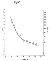
- the measured variation in ⁇ over the wavelength range ⁇ 1.49 to 1.57 ⁇ m (0.791 to 0.833 eV) is shown in Figure 2.
- the left hand vertical axis is ⁇ while the right hand axis is the linewidth broadening term (1 + ⁇ 2) disclosed by Charles H Henry.
- ⁇ can be seen to increase rapidly as the photon energy approaches the band gap energy, 0.791 eV.
- the curve illustrates the advantage that can be gained by operating a laser at a wavelength below ⁇ max.
- ⁇ max ie. at 0.811 eV
- ⁇ max 5.1.
- ⁇ 0.9 ⁇ max.
- ⁇ can be reduced to values of 0.8 ⁇ max and 0.7 ⁇ max respectively.
- the emission linewidth of a laser depends on many factors and the effect of a reduction in ⁇ can be heavily obscured, or even more than cancelled out, by other factors in the design or operation of a laser. For instance, operating temperature has a strong influence on linewidth, increasing temperature resulting in increased linewidth.
- the figures for linewidth given relate to laser structures which are heat-stabilised in operation, by known techniques.
- the emission radiation has a wavelength which lies in the range 1.1 to 1.65 ⁇ m, to operate at a wavelength 40 to 80nm, and particularly 60 nm, shorter than ⁇ max for a particular laser structure. This gives a significant reduction in emission linewidth without increasing the threshold current of the laser too high.
- the reduction in linewidth which can usefully be obtained by operating a laser structure at a wavelength below ⁇ max is generally of the order of 50%.
Landscapes
- Physics & Mathematics (AREA)
- Condensed Matter Physics & Semiconductors (AREA)
- General Physics & Mathematics (AREA)
- Electromagnetism (AREA)
- Optics & Photonics (AREA)
- Geometry (AREA)
- Semiconductor Lasers (AREA)
- Radiation-Therapy Devices (AREA)
Claims (8)
- Laseranordnung, die eine Halbleiterlaserstruktur und eine Einrichtung zum Auswählen der Emissionswellenlänge λe der Laserstruktur aufweist, wobei die ausgewählte Wellenlänge kürzer als die Wellenlänge λmax eines maximalen Verstärkungsfaktors beim Schwellenstrom ist,
dadurch gekennzeichnet, daß
die Einrichtung nicht aus einem Fabry-Perot-Resonator besteht, der zwischen zwei Endkristallflächen der Halbleiterlaserstruktur gebildet ist, daß λe in einem der Bereiche 1,2 bis 1,35 µm und 1,48 bis 1,65 µm liegt, und daß die gewählte Wellenlänge kürzer als λmax ist, und zwar um einen Betrag, so daß der Linienbreiten-Schärfefaktor αmax bei λmax, und der Linienbreiten-Schärfefaktor αe bei der Wellenlänge der emittierten Strahlung in der folgenden Weise in Relation stehen:

- Laseranordnung nach Anspruch 1, wobei die Auswähleinrichtung ein Gitter aufweist, das innerhalb der Halbleiterstruktur gebildet ist.
- Laseranordnung nach Anspruch 2, wobei die Laserstruktur ein Laser mit verteilter Rückkopplung (DFB) ist, und wobei das Gitter eine verteilte optische Rückkopplung innerhalb der Laserstruktur bereitstellt.
- Laseranordnung nach einem der vorhergehenden Ansprüche, wobei αmax und αe in der folgenden Weise in Relation sind:

- Laseranordnung nach Anspruch 4, wobei αmax und αe in der folgenden Weise in Relation stehen:

- Laseranordnung nach einem der vorhergehenden Ansprüche, wobei die Einrichtung zum Auswählen der Emissionswellenlänge der Halbleiterstruktur einen externen Resonator aufweist.
- Laseranordnung nach Anspruch 6, wobei die Einrichtung weiterhin ein Gitter für verteilte Rückkoppelung aufweist.
- Kohärentes optisches Kommunikationssystem, das mindestens eine Halbleiterlaseranordnung nach einem der Ansprüche 1 bis 7 aufweist.
Priority Applications (1)
| Application Number | Priority Date | Filing Date | Title |
|---|---|---|---|
| AT86306427T ATE96252T1 (de) | 1985-09-09 | 1986-08-19 | Halbleiterlaser. |
Applications Claiming Priority (2)
| Application Number | Priority Date | Filing Date | Title |
|---|---|---|---|
| GB858522308A GB8522308D0 (en) | 1985-09-09 | 1985-09-09 | Semiconductor lasers |
| GB8522308 | 1985-09-09 |
Publications (2)
| Publication Number | Publication Date |
|---|---|
| EP0218344A1 EP0218344A1 (de) | 1987-04-15 |
| EP0218344B1 true EP0218344B1 (de) | 1993-10-20 |
Family
ID=10584913
Family Applications (1)
| Application Number | Title | Priority Date | Filing Date |
|---|---|---|---|
| EP86306427A Expired - Lifetime EP0218344B1 (de) | 1985-09-09 | 1986-08-19 | Halbleiterlaser |
Country Status (9)
| Country | Link |
|---|---|
| US (1) | US4754459A (de) |
| EP (1) | EP0218344B1 (de) |
| JP (1) | JPH0744308B2 (de) |
| AT (1) | ATE96252T1 (de) |
| CA (1) | CA1265604A (de) |
| DE (1) | DE3689188T2 (de) |
| ES (1) | ES2001941A6 (de) |
| GB (1) | GB8522308D0 (de) |
| HK (1) | HK135396A (de) |
Families Citing this family (24)
| Publication number | Priority date | Publication date | Assignee | Title |
|---|---|---|---|---|
| JPS62257783A (ja) * | 1986-04-30 | 1987-11-10 | Sharp Corp | 半導体レ−ザ素子 |
| FR2605801B1 (fr) * | 1986-10-23 | 1989-03-03 | Menigaux Louis | Procede de fabrication d'une structure semi-conductrice susceptible d'effet laser multi-longueurs d'onde, et dispositif obtenu |
| GB2203891A (en) * | 1987-04-21 | 1988-10-26 | Plessey Co Plc | Semiconductor diode laser array |
| US5119393A (en) * | 1989-06-14 | 1992-06-02 | Hitachi, Ltd. | Semiconductor laser device capable of controlling wavelength shift |
| US5317588A (en) * | 1992-11-05 | 1994-05-31 | Eastman Kodak Company | Ridge waveguide distributed-feedback laser diode with a depressed-index cladding layer |
| US5305340A (en) * | 1992-12-16 | 1994-04-19 | International Business Machines Corporation | Waveguide ridge laser device with improved mounting and ridge protection |
| US6330265B1 (en) * | 1998-04-21 | 2001-12-11 | Kabushiki Kaisha Toshiba | Optical functional element and transmission device |
| EP1343232B1 (de) * | 2002-03-08 | 2007-05-02 | nanoplus GmbH Nanosystems and Technologies | Ein Halbleiterlaserarray mit seitlicher Gratingstruktur |
| TWI225723B (en) * | 2002-04-12 | 2004-12-21 | Univ Nat Taiwan | Two-pole different width multi-layered semiconductor quantum well laser with carrier redistribution to modulate light-emission wavelength |
| US7613401B2 (en) * | 2002-12-03 | 2009-11-03 | Finisar Corporation | Optical FM source based on intra-cavity phase and amplitude modulation in lasers |
| US8792531B2 (en) | 2003-02-25 | 2014-07-29 | Finisar Corporation | Optical beam steering for tunable laser applications |
| WO2008080171A1 (en) * | 2006-12-22 | 2008-07-03 | Finisar Corporation | Optical transmitter having a widely tunable directly modulated laser and periodic optical spectrum reshaping element |
| US7941057B2 (en) * | 2006-12-28 | 2011-05-10 | Finisar Corporation | Integral phase rule for reducing dispersion errors in an adiabatically chirped amplitude modulated signal |
| US8131157B2 (en) | 2007-01-22 | 2012-03-06 | Finisar Corporation | Method and apparatus for generating signals with increased dispersion tolerance using a directly modulated laser transmitter |
| WO2008097928A1 (en) * | 2007-02-02 | 2008-08-14 | Finisar Corporation | Temperature stabilizing packaging for optoelectronic components in a transmitter module |
| US8027593B2 (en) | 2007-02-08 | 2011-09-27 | Finisar Corporation | Slow chirp compensation for enhanced signal bandwidth and transmission performances in directly modulated lasers |
| US7991291B2 (en) * | 2007-02-08 | 2011-08-02 | Finisar Corporation | WDM PON based on DML |
| JP4312239B2 (ja) * | 2007-02-16 | 2009-08-12 | 富士通株式会社 | 光素子及びその製造方法 |
| US7991297B2 (en) | 2007-04-06 | 2011-08-02 | Finisar Corporation | Chirped laser with passive filter element for differential phase shift keying generation |
| US8204386B2 (en) | 2007-04-06 | 2012-06-19 | Finisar Corporation | Chirped laser with passive filter element for differential phase shift keying generation |
| US8160455B2 (en) * | 2008-01-22 | 2012-04-17 | Finisar Corporation | Method and apparatus for generating signals with increased dispersion tolerance using a directly modulated laser transmitter |
| US8260150B2 (en) | 2008-04-25 | 2012-09-04 | Finisar Corporation | Passive wave division multiplexed transmitter having a directly modulated laser array |
| US8199785B2 (en) * | 2009-06-30 | 2012-06-12 | Finisar Corporation | Thermal chirp compensation in a chirp managed laser |
| DE102009054592A1 (de) * | 2009-12-14 | 2011-06-16 | Dr. Johannes Heidenhain Gmbh | Positionsmesseinrichtung |
-
1985
- 1985-09-09 GB GB858522308A patent/GB8522308D0/en active Pending
- 1985-10-07 US US06/784,949 patent/US4754459A/en not_active Expired - Lifetime
-
1986
- 1986-08-13 CA CA000515884A patent/CA1265604A/en not_active Expired - Lifetime
- 1986-08-19 EP EP86306427A patent/EP0218344B1/de not_active Expired - Lifetime
- 1986-08-19 DE DE86306427T patent/DE3689188T2/de not_active Expired - Lifetime
- 1986-08-19 AT AT86306427T patent/ATE96252T1/de not_active IP Right Cessation
- 1986-09-05 ES ES8601670A patent/ES2001941A6/es not_active Expired
- 1986-09-09 JP JP61213688A patent/JPH0744308B2/ja not_active Expired - Lifetime
-
1996
- 1996-07-25 HK HK135396A patent/HK135396A/en not_active IP Right Cessation
Non-Patent Citations (1)
| Title |
|---|
| ELECTRONIC LETTERS, vol. 22, No. 11, May 1986, pages 580-581 * |
Also Published As
| Publication number | Publication date |
|---|---|
| CA1265604A (en) | 1990-02-06 |
| JPH0744308B2 (ja) | 1995-05-15 |
| DE3689188D1 (de) | 1993-11-25 |
| US4754459A (en) | 1988-06-28 |
| JPS6261387A (ja) | 1987-03-18 |
| ATE96252T1 (de) | 1993-11-15 |
| GB8522308D0 (en) | 1985-10-16 |
| EP0218344A1 (de) | 1987-04-15 |
| ES2001941A6 (es) | 1988-07-01 |
| DE3689188T2 (de) | 1994-03-03 |
| HK135396A (en) | 1996-08-02 |
Similar Documents
| Publication | Publication Date | Title |
|---|---|---|
| EP0218344B1 (de) | Halbleiterlaser | |
| US4964134A (en) | Semiconductor laser structures | |
| Burnham et al. | Single-heterostructure distributed-feedback GaAs-diode lasers | |
| US6026110A (en) | Distributed feedback semiconductor laser with gain modulation | |
| US7586970B2 (en) | High efficiency partial distributed feedback (p-DFB) laser | |
| US4701930A (en) | Distributed feedback semiconductor laser | |
| Carlson et al. | Mode discrimination in distributed feedback grating surface emitting lasers containing a buried second-order grating | |
| Takemoto et al. | 1.3-mu m distributed feedback laser diode with a grating accurately controlled by a new fabrication technique | |
| Lammert et al. | Low-threshold narrow-linewidth InGaAs-GaAs ridge-waveguide DBR lasers with first-order surface gratings | |
| EP0254311B1 (de) | Laserdiode mit verteilter Rückkopplung | |
| Itaya et al. | Longitudinal mode behaviors of 1.5 µm range GaInAsP/InP distributed feedback lasers | |
| JP5099948B2 (ja) | 分布帰還型半導体レーザ素子 | |
| US6370219B1 (en) | Self-modulated, filament-based, solid state laser | |
| Kobayashi et al. | High light output-power single-longitudinal-mode semiconductor laser diodes | |
| EP0468482B1 (de) | Halbleiterlaser | |
| US7072373B2 (en) | Ridge waveguide semiconductor laser diode | |
| US7627012B2 (en) | Distributed feedback semiconductor laser including wavelength monitoring section | |
| US8121170B2 (en) | Gain-coupled distributed feedback semiconductor laser including first-order and second-order gratings | |
| US5556795A (en) | Quantum well superluminescent diode | |
| Osowski et al. | An asymmetric cladding gain-coupled DFB laser with oxide defined metal surface grating by MOCVD | |
| JPS63228795A (ja) | 分布帰還型半導体レ−ザ | |
| Noda et al. | Ridge waveguide AlGaAs/GaAs distributed feedback lasers with multiple quantum well structure | |
| Wang et al. | Low-chirp and high-power 1.55-μm strained-quantum-well complex-coupled DFB laser | |
| Takahashi et al. | Narrow spectral linewidth 1.5 mu m GaInAsP/InP distributed Bragg reflector (DBR) lasers | |
| Kapon et al. | Distributed Bragg-reflector Pb 1-x Sn x Te/PbSe y Te 1-y diode lasers |
Legal Events
| Date | Code | Title | Description |
|---|---|---|---|
| PUAI | Public reference made under article 153(3) epc to a published international application that has entered the european phase |
Free format text: ORIGINAL CODE: 0009012 |
|
| AK | Designated contracting states |
Kind code of ref document: A1 Designated state(s): AT BE CH DE FR GB IT LI LU NL SE |
|
| 17P | Request for examination filed |
Effective date: 19871012 |
|
| RAP3 | Party data changed (applicant data changed or rights of an application transferred) |
Owner name: BRITISH TELECOMMUNICATIONS PUBLIC LIMITED COMPANY |
|
| 17Q | First examination report despatched |
Effective date: 19900123 |
|
| GRAA | (expected) grant |
Free format text: ORIGINAL CODE: 0009210 |
|
| AK | Designated contracting states |
Kind code of ref document: B1 Designated state(s): AT BE CH DE FR GB IT LI LU NL SE |
|
| PG25 | Lapsed in a contracting state [announced via postgrant information from national office to epo] |
Ref country code: LI Effective date: 19931020 Ref country code: BE Effective date: 19931020 Ref country code: AT Effective date: 19931020 Ref country code: CH Effective date: 19931020 |
|
| REF | Corresponds to: |
Ref document number: 96252 Country of ref document: AT Date of ref document: 19931115 Kind code of ref document: T |
|
| ITF | It: translation for a ep patent filed | ||
| REF | Corresponds to: |
Ref document number: 3689188 Country of ref document: DE Date of ref document: 19931125 |
|
| REG | Reference to a national code |
Ref country code: CH Ref legal event code: PL |
|
| ET | Fr: translation filed | ||
| PLBE | No opposition filed within time limit |
Free format text: ORIGINAL CODE: 0009261 |
|
| STAA | Information on the status of an ep patent application or granted ep patent |
Free format text: STATUS: NO OPPOSITION FILED WITHIN TIME LIMIT |
|
| PG25 | Lapsed in a contracting state [announced via postgrant information from national office to epo] |
Ref country code: LU Free format text: LAPSE BECAUSE OF NON-PAYMENT OF DUE FEES Effective date: 19940831 |
|
| 26N | No opposition filed | ||
| EAL | Se: european patent in force in sweden |
Ref document number: 86306427.5 |
|
| REG | Reference to a national code |
Ref country code: GB Ref legal event code: 732E |
|
| REG | Reference to a national code |
Ref country code: GB Ref legal event code: IF02 |
|
| REG | Reference to a national code |
Ref country code: GB Ref legal event code: 732E |
|
| PGFP | Annual fee paid to national office [announced via postgrant information from national office to epo] |
Ref country code: FR Payment date: 20050711 Year of fee payment: 20 |
|
| PGFP | Annual fee paid to national office [announced via postgrant information from national office to epo] |
Ref country code: NL Payment date: 20050713 Year of fee payment: 20 Ref country code: GB Payment date: 20050713 Year of fee payment: 20 |
|
| PGFP | Annual fee paid to national office [announced via postgrant information from national office to epo] |
Ref country code: DE Payment date: 20050715 Year of fee payment: 20 |
|
| PGFP | Annual fee paid to national office [announced via postgrant information from national office to epo] |
Ref country code: SE Payment date: 20050719 Year of fee payment: 20 |
|
| PGFP | Annual fee paid to national office [announced via postgrant information from national office to epo] |
Ref country code: IT Payment date: 20050721 Year of fee payment: 20 |
|
| PG25 | Lapsed in a contracting state [announced via postgrant information from national office to epo] |
Ref country code: GB Free format text: LAPSE BECAUSE OF EXPIRATION OF PROTECTION Effective date: 20060818 |
|
| PG25 | Lapsed in a contracting state [announced via postgrant information from national office to epo] |
Ref country code: NL Free format text: LAPSE BECAUSE OF EXPIRATION OF PROTECTION Effective date: 20060819 |
|
| REG | Reference to a national code |
Ref country code: GB Ref legal event code: PE20 |
|
| NLV7 | Nl: ceased due to reaching the maximum lifetime of a patent |
Effective date: 20060819 |
|
| EUG | Se: european patent has lapsed |