EP0220571B1 - Procédé et appareil d'alignement - Google Patents
Procédé et appareil d'alignement Download PDFInfo
- Publication number
- EP0220571B1 EP0220571B1 EP86114040A EP86114040A EP0220571B1 EP 0220571 B1 EP0220571 B1 EP 0220571B1 EP 86114040 A EP86114040 A EP 86114040A EP 86114040 A EP86114040 A EP 86114040A EP 0220571 B1 EP0220571 B1 EP 0220571B1
- Authority
- EP
- European Patent Office
- Prior art keywords
- mask
- alignment
- wafer
- alignment pattern
- pattern
- Prior art date
- Legal status (The legal status is an assumption and is not a legal conclusion. Google has not performed a legal analysis and makes no representation as to the accuracy of the status listed.)
- Expired
Links
- 238000000034 method Methods 0.000 title claims description 24
- 230000003287 optical effect Effects 0.000 claims description 65
- 238000001514 detection method Methods 0.000 claims description 50
- 238000005286 illumination Methods 0.000 claims description 18
- 238000003384 imaging method Methods 0.000 claims description 10
- 238000006073 displacement reaction Methods 0.000 claims description 8
- 230000000873 masking effect Effects 0.000 claims description 7
- 230000015572 biosynthetic process Effects 0.000 claims description 6
- 230000002093 peripheral effect Effects 0.000 claims description 2
- 238000006243 chemical reaction Methods 0.000 claims 3
- 238000012935 Averaging Methods 0.000 claims 2
- 230000001131 transforming effect Effects 0.000 claims 1
- 238000010586 diagram Methods 0.000 description 20
- 238000007906 compression Methods 0.000 description 6
- 230000006870 function Effects 0.000 description 6
- 230000006835 compression Effects 0.000 description 5
- 238000005070 sampling Methods 0.000 description 5
- 239000000835 fiber Substances 0.000 description 3
- 230000008569 process Effects 0.000 description 3
- 230000006866 deterioration Effects 0.000 description 2
- 238000000605 extraction Methods 0.000 description 2
- 239000012528 membrane Substances 0.000 description 2
- 230000004044 response Effects 0.000 description 2
- 230000003213 activating effect Effects 0.000 description 1
- 230000001427 coherent effect Effects 0.000 description 1
- 125000004122 cyclic group Chemical group 0.000 description 1
- 230000001771 impaired effect Effects 0.000 description 1
- 230000010354 integration Effects 0.000 description 1
- 230000007246 mechanism Effects 0.000 description 1
- 230000009467 reduction Effects 0.000 description 1
- 239000004065 semiconductor Substances 0.000 description 1
Images


Classifications
-
- G—PHYSICS
- G03—PHOTOGRAPHY; CINEMATOGRAPHY; ANALOGOUS TECHNIQUES USING WAVES OTHER THAN OPTICAL WAVES; ELECTROGRAPHY; HOLOGRAPHY
- G03F—PHOTOMECHANICAL PRODUCTION OF TEXTURED OR PATTERNED SURFACES, e.g. FOR PRINTING, FOR PROCESSING OF SEMICONDUCTOR DEVICES; MATERIALS THEREFOR; ORIGINALS THEREFOR; APPARATUS SPECIALLY ADAPTED THEREFOR
- G03F9/00—Registration or positioning of originals, masks, frames, photographic sheets or textured or patterned surfaces, e.g. automatically
- G03F9/70—Registration or positioning of originals, masks, frames, photographic sheets or textured or patterned surfaces, e.g. automatically for microlithography
Definitions
- This invention relates to a method and apparatus for aligning a plurality of objects, e.g., a wafer and mask, overlapping closely each other by measuring the relative displacement of the objects, and the invention particularly relates to a method and apparatus for alignment suitable for a proximity aligner system such as an X-ray exposure system in order to expose both the mask and the wafer.
- a proximity aligner system such as an X-ray exposure system
- the X-ray aligner which is a typical proximity aligner is intended to deal with a line width smaller than 0.8 1 1m.
- the alignment accuracy as fine as 0.3 11m is now required.
- Methods of alignment detection include magnification of the alignment pattern, scanning of the alignment pattern using a laser beam and alignment method using a diffraction grating.
- the first-mentioned method is that alignment patterns of the mask and wafer are magnified by the objective lens and focused on the imaging element, the relative displacement of both patterns is evaluated through the signal processing, and the wafer is moved relative to the mask so that the relative displacement does not exist.
- the above-mentioned 0.3 11m alignment accuracy includes the mechanical error of the aligner and the dimensional error of the mask and wafer, and therefore the pure alignment accuracy required is as high as 0.1 11m.
- the fresnel zone marks made on the mask and wafer are illuminated oblique from outside of the exposure area into the exposure area so that the coherent light diffracted in the fresnel zone focuses in the exposure area, and therefore the objective lens for detecting the focal position must be located in the exposure area. Accordingly, the focal point in the fresnel zone is detected by the objective lens and, after alignment of the wafer to the mask, the objective lens must be retracted.
- the conventional exposing method has employed a single exposing operation for the entire surface of a wafer, and a slight overhead time has not been a serious matter. A positioning method of this category is disclosed in U.S. Patent Application Serial No. 139,544 (US-A 4 326 805).
- the alignment and exposing operations are repeated more than ten times for each wafer, and the reduction of the alignment time is an urgent request.
- An associated problem is the deterioration of the mask-wafer alignment accuracy due to the vibration when the objective lens is moved following each mask-wafer alignment operation.
- An object of this invention is to provide a method and apparatus for alignment, in which the objective lens of a microscope for viewing a mask and wafer does not interfere with the exposure light, e.g., X-ray, so that the microscope objective lens does not need to retract, thereby improving the throughput, and the position of the mask and wafer can be detected during exposure, and moreover the alignment mark on the mask is detected accurately, whereby accurate alignment can be accomplished.
- the exposure light e.g., X-ray
- the inventive apparatus is arranged to have its microscope objective lens inclined with respect to the normal of the detection plane, i.e., the mask plane or wafer plane, so that the lens does not interfere with the exposure light, e.g., X-ray, thereby allowing the image transfer while detecting the relative position between the mask and wafer, and is provided with a mask alignment pattern which is formed of a pluraliry of linear segments oriented in one direction so that the mask alignment pattern without the shadow can be made longer, and is adapted to receive image signals across the linear segments, thereby improving the accuracy of positional detection of the mask alignment pattern, whereby as a result the mask-wafer alignment accuracy is upgraded.
- the detection plane i.e., the mask plane or wafer plane
- the detection plane of the microscope objective lens is not perpendicular to the detection optical axis, and therefore when it is detected by the microscope objective lens, the imaging plane becomes more oblique against the optical axis.
- the optical sensor for positional detection is placed at right angles with the optical axis, the in-focus portion is only a fraction of the whole and sufficient positional information cannot be obtained.
- a diffraction grating having a grating face in a certain shape is disposed virtually in coincidence with the imaging plane which is oblique with respect to the optical axis.
- the imaging plane intersects the optical axis virtually at right angles.
- an objective lens with small NA (Numerical Aperture) is used to make up a magnification optical system. Since an objective lens with small NA has a longer operating distance and a deeper focal depth, it becomes possible to detect the alignment pattern in an oblique arrangement so that is does not interfere with the exposure light even in detecting a pattern in the exposure area or its periphery. However, positional detection is in only one direction for an optical axis (the direction at right angles with the detection optical axis on the wafer or mask plane), and therefore three optical axes are required for three-dimensional detection (X, Y, e) for example.
- X, Y, e three-dimensional detection
- the mask alignment pattern is formed of a plurality of linear segments oriented in one direction so that the pattern without the shadow can be made longer and the image signals across the linear segment are received, with the intention of improving the accuracy of positional detection of the mask alignment pattern.
- Fig. 1 A is a front view showing in brief the arrangement of the inventive mask alignment apparatus
- Fig. 1 B is a plan view pertinent to Fig. 1A.
- a wafer 1 has a formation of a wafer pattern (not shown) on its upper surface.
- a mask 3 is made of a transparent sheet and disposed in parallel to the wafer 1 with a spacing of 10-15 11m.
- the mask 3 has on its upper surface a formation of three alignment patterns 7 on streets 6 within a chip 5, and has on its lower surface a formation of a mask pattern (not shown) in location coincident with the wafer pattern.
- An exposure X-ray beam 4 is emitted from an X-ray source (not shown) located above the mask 3, and it is intended to project the mask pattern on to an area of 30 mm square, for example, on the wafer 1.
- Reference number 8 generally denotes three sets of lillumination optical systems (only one set is shown in the figure), and each system operates such that the white illumination light produced by a light source 9 is conducted through a fiber 10a, lens 11, filter 10b, diaphragms 12a and 12b, and a lens 13 to a mirror 14, which is disposed outside the field of the exposure X-ray beam 4 so that the illumination light beam irradiates the wafer alignment pattern and mask alignment pattern along the illumination optical axis 16 that inclines by about 20 ° with respect to the plane at right angles with the alignment direction (Y direction), i.e., with respect to the normal 15.
- Reference number 20 generally denotes three sets of detection optical systems (only one set is shown in the figure), and each system consists of an objective lens 21, a mirror 22, a focusing lens 23, a TV camera 25, a monitor TV set 26, and a processing circuit 27.
- the image displayed on the monitor TV screen 25 is such that the mask pattern 19 at a latelally center position is best in-focus at the left-hand intersection MF and the pattern goes out of focus as the position moves to both longitudinal directions, while two wafer patterns 18 on both sides of the central mask pattern 19 is best in-focus at the right-hand intersection WF and the pattern goes out of focus as the position moves to both longitudinal directions.
- the range L between the intersections MF and WF is calculated to be 26.3 11m in terms of the view field based on the result of Table 1. The availability of such a large in-focus range L owes to the smaller NA of the objective lens 21.
- the performance of the objective lens is given as functions of NA as follows. where is the wavelength of the light used. As indicated, the smaller the NA, the larger is the operating distance.
- Table 1 is the result of calculation of the above equations (1) and (2) for NA taking values 0.25 and 0.5.
- the present invention employs an objective lens with smaller NA in the magnification optical system.
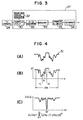
- the processing circuit 27 in Fig. 1A is shown in more detail In Fig. 3, in which a sample-holding circuit 30 operates in response to a video signal 31 as shown in Fig. 4(A) to sample the signal at a constant interval to sampling positions x1, x2, ..., xn and hold the respective signal levels y1, y2, ..., yn as shown in Fig: 4(B).
- a sampling signal generator 32 provides the sampling signal for the sample-holding circuit 30.
- An A/D converter 33 converts the analog signal held in the sample-holding circuit 30 into digital data.
- a memory 34 stores temporarily the digital data y1, y2, ..., yn provided by the AID converter 33.
- An operational circuit 35 calculates the symmetry function Zi(xi) given by the following equation (3) with respect to ⁇ j sampling positions centered by point xi as a point of symmetry as shown in Fig. 4(B).
- m is a value determined optimally in consideration of the dimensions of the position alignment pattern in attention on the wafer 1 as shown in Fig. 4(B).
- the operational circuit 35 calculates the symmetry function Zi(xi) as shown in Fig. 4(C) by moving the symmetric point xi from x1 to x2 and up to xn, and detects a symmetric point xo which minimizes the function.
- the processing circuit 27 further includes an interface 54 for sending the alignment value from the operational circuit 35 to the motor driver shown in Fig. 1.
- the processing circuit 27 operates such that the TV camera 25 transforms an image as shown in Fig. 2(B) into a video signal 31 shown in Fig. 4(A), the sample-holding circuit 30 takes samples of the video signal 31 at a constant interval, the AID converter 33 converts held value y1, y2, ..., yn into digital data y1, y2, ..., yn, and the operational circuit 35 calculates the symmetry function Zi(xi) given by the equation (3) for ⁇ j sampling positions centered by symmetric point xi, while moving the symmetric point from x1, x2, ..., xn successively, as shown in Fig.
- the present invention allows concurrent focusing for the mask alignment pattern 19 and wafer alignment pattern 18, as described in connection with Fig. 2A, and therefore a double focal point can be realized using the single optical system.
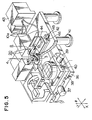
- Fig. 5 is a perspective view of the apparatus for detecting the relative position of objects according to an embodiment of this invention.
- an X table 38 is supported on a base 36 so that it is moved in the X direction by an X-axis driving motor 37
- a Y table 40 is supported on the X table 38 so that it is moved in the Y direction by a Y-axis driving motor 39
- the wafer 1 shown in Fig. 1 is mounted on the Y table 40.
- a platform 42 is fixed over the waver 1 by means of feet 41, and the aforementioned mask 3 is fixed on the platform 42 above the wafer 1.
- the aforementioned three sets of illumination optical systems 8 and three sets of detection optical systems 20 are disposed in a radial formation around the mask 3 on the platform 42, and the three sets of illunimation optical systems 8 are linked through respective fibers 10a to an Xe lamp house 43 which is supported independently of the platform 42.
- the three sets of illumination optical systems 8 activated by the Xe lamp house 43 through the three fibers 10a operate to irradiate the mask 3 and wafer 1 concurrently
- the three sets of detection optical systems 20 operate to detect alignment errors between the wafer 1 and mask 3 in the X, Y and e directions concurrently so as to move the X table 38 and Y table 40 in response to the detected alignment errors, thereby aligning the wafer 1 with the mask 3.
- Fig. 6 is a perspective view showing in detail a set of the illumination optical system 8 and detection optical system 20 shown in Fig. 5.
- both the illumination optical system 8 and detection optical system 20 are supported on a common table 44, which is supported on a table 46 so that it is moved in the radial direction of the mask 3 by a driving motor 45, and the table 46 is supported fixedly on the platform 42 shown in Fig. 5.
- This arrangement allows both the illumination optical system 8 and detection optical system 20 to move concurrently in the radial direction over the mask 3.
- the positioning operation can take place for the alignment pattern 47 for multiple sequential processes existing on the street 6 formed within the chip 5 on the mask 3.
- the sequential positioning operation can take place for various sizes of the chip 5.
- FIGs. 7(A) to 7(D) show embodiments of the detection pattern.
- each of detection patterns 19a - 19d is formed of many detection pattern segments 50 by the following reason.
- a wafer 1 and mask 3 are placed in parallel to each other with a spacing of 10 1 1m for example, and a mask pattern 19 on the lower surface of the mask 3 is illuminated by the light having an optical axis 13 inclined by angle e with respect to the normal 15 which is at right angles with the alignment plane of the wafer 1 and mask 3, with the result of the creation of a shadow 51 of the mask pattern 19 on the wafer 1, as shown in Fig. 8B.
- the shadow 51 is created to surround part of the mask pattern 19, and in this state the center of the positioning pattern is obtained as shown in Fig. 4(C) by the processing circuit 27 shown in Fig. 3.
- the signal shown in Fig. 9C obtained from a distortion of the mask pattern 19 or signal noise in correspondence to a raster of the TV camera 25 shown in Figs. 9A and 9B cannot provide accurate positional information in many cases.
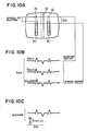
- the AID converter 18 transforms the signal levels into digital data
- the memory 34 stores temporality the digital data
- the operational circuit 35 calculates the sum of the digital data as shown in Fig. 10B and calculates the mean value as shown in Fig. 10C, and finally the symmetric point porviding a minimum value is obtained.
- the TV camera 25 shoots the mask pattern 19 and shadow image 51 concurrently during the scanning of the m-raster band, and therefore the accuracy of detecting the position of the mask pattern 19 is deteriorated.
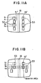
- the mask pattern 19 is formed of a plurality of linear mask pattern segments 50 with a spacing 49 equal in dimension to the shadow image 51 so that images 19' and shadow images 51 are placed alternately as shown in Fig. 11 A, thereby preventing the shadow image 51 from entering to the image of each mask pattern segment 50.
- the pattern entry area is restricted so that the influence of the shadow is avoided.
- alignment detection is carried out manually or by means of the detection system and processing circuit 27 shown in Fig. 1 so that the mask pattern is included within a predetermined area 53 on the screen, and then positioning is carried out by activating a motor 52-1 using a driver 53-1.
- the operational circuit 35 implements the alignment process by following the procedure shown in Fig. 16.
- the sum of the signals is calculated as shown in Fig. 12B for the predetermined areas S1 - E1 and S2 - E2 as shown in Fig. 12A in the same method as described in Fig. 10, the mean value is calculated as shown in Fig. 12C, and only the mask pattern is extracted by masking off the portion of the wafer pattern as shown in Fig. 12D.
- the sum of the signals is calculated as shown in Fig. 13B for the predetermined areas S3 - E3 as shown in Fig. 13A by the same method described in Fig. 10, the mean value is calculated as shown in Fig. 13C, and only the wafer pattern is extracted by masking off the portion of the mask pattern as shown in Fig. 13D.
- the mask-pattern positioning operation is carried out by means of the driver 53 and motor 52 shown in Fig. 1.
- Fig. 7(A) shows the case where a mask alignment pattern 19a in the form of a dashed line and two linear wafer alignment pattern 18a located symmetrically on both sides of 19a are arranged on and in parallel to the optical axis plane 48.
- Fig. 7(B) shows the case where a dashed-line mask alignment pattern 19b and two linear wafer alignment patterns and three mask alignment patterns 19b located alternately and symmetrically on both sides of 19b are arranged on and in parallel to the optical axis plane 48.
- Fig. 7(B) shows the case where a dashed-line mask alignment pattern 19b and two linear wafer alignment patterns and three mask alignment patterns 19b located alternately and symmetrically on both sides of 19b are arranged on and in parallel to the optical axis plane 48.
- FIG. 7(C) shows the case where a linear wafer alignment pattern 18c and two sets of linear wafer alignment patterns 18c located symmetrically on both sides of the first-mentioned 18c are arranged, with three dashed-line mask alignment patterns 19c having a smaller dimension in the longitudinal direction of the optical axis plane 48 being disposed in the central portion of the above three sets of wafer alignment patterns 18c, are arranged on and in parallel to the optical axis plane 48.
- Fig. 7(D) shows the case where linear wafer alignment patterns 18d and dashed-line mask alignment patterns 19g and 19h are arranged in parallel to the optical axis on the optical axis plane 48.
- FIG. 7(E) shows the case where a dashed-line mask alignment pattern 19e and two linear wafer alignment patterns 18e located oblique and symmetrically with respect to the optical axis plane 48 on both sides of 19e are arranged on and in parallel to the optical axis plane 48.
- the inventive method is capable of alignment detection provided that patterns are arranged symmetrically with respect to the plane parallel to the optical axis plane 48 (i.e., the plane at right angles with the drawing).
- the optical axis plane 48 may have a parallel displacement within the figure. The reason is that for the case of a plane in other direction than mentioned above, the foregoing inventive method, which implements detection in a direction inclined with respect to the alignment plane, is incapable of accurate alignment detection due to the occurrence of asymmetry for planes other than that in parallel to the optical axis plane 46.
- Figs. 15A through 15C show the directions of detection for three sets of alignment patterns 49a, 49b and 49c, each set made up of a central mask alignment pattern 19j and two wafer alignment patterns 18i located symmetrically on both sides of 19j.
- Fig. 15A shows the case where a set of alignment patterns 49a are placed on a center line 0 2 in the Y direction so that a mask alignment pattern 19j and two wafer alignment patterns 18i are arranged in the X direction and other two sets of alignment patterns 49b and 49c each including a mask alignment pattern 19j and two wafer alignment patterns 18i are placed on a center line 0 3 in the X direction, with the distance of these sets of alignment patterns from the center 0 1 of the wafer 1 and mask 3 being made equal.
- Fig. 15B shows the case where among four planes H, I, J and K partitioned by a center line 0 3 in the X direction and a center line 0 2 in the Y direction both passing through the center 0 1 of the wafer 1 and mask 3, three sets of alignment patterns 49a, 49b and 49c are placed on the planes I, J and K, respectively, so that a mask aligment pattern 19i and two wafer alignment patterns 18i are arranged in the X direction for each of the alignment pattern sets 49a and 49b placed on planes I and J, and a mask alignment pattern 19i and two wafer alignment patterns 18i are arranged in the Y direction for the alignment pattern set 49c placed on plane K.
- Fig. 15B shows the case where among four planes H, I, J and K partitioned by a center line 0 3 in the X direction and a center line 0 2 in the Y direction both passing through the center 0 1 of the wafer 1 and mask 3, three sets of alignment patterns 49a, 49b and
- 15C shows the case where three sets of alignment patterns 49a, 49b and 49c are placed radially with respect to the center 0 1 , so that a mask alignment pattern 10i and two wafer alignment patterns 18i are arranged in the Y direction for the alignment pattern set 49a, and a mask alignment pattern 19i and two wafer alignment patterns 18i are arranged in the oblique direction for each of the alignment pattern sets 49b and 49c.
- arrangement may be made so that three-dimensional detection is implemented using three sets of alignment patterns.
- each illumination optical system has its optical axis provided symmetrically against the optical axis of the detection optical system
- the dark field illumination, illumination from the objective lens, or combination of these may be employed.
- the X-ray beam is used for the exposure light
- the present invention is not confined to this, but a corpuscular beam or white light beam can also be used. It is not necessary to place an alignment pattern exclusively, but an image created in proximity to the wafer and mask can be used.
- the objective lens is preferably one having NA of below 0.4, and the inclination of the detection optical axis is preferably smaller than 70 ° .
Landscapes
- Physics & Mathematics (AREA)
- General Physics & Mathematics (AREA)
- Exposure And Positioning Against Photoresist Photosensitive Materials (AREA)
- Exposure Of Semiconductors, Excluding Electron Or Ion Beam Exposure (AREA)
Claims (5)
Applications Claiming Priority (2)
| Application Number | Priority Date | Filing Date | Title |
|---|---|---|---|
| JP226999/85 | 1985-10-14 | ||
| JP60226999A JPH0666241B2 (ja) | 1985-10-14 | 1985-10-14 | 位置検出方法 |
Publications (2)
| Publication Number | Publication Date |
|---|---|
| EP0220571A1 EP0220571A1 (fr) | 1987-05-06 |
| EP0220571B1 true EP0220571B1 (fr) | 1990-06-13 |
Family
ID=16853922
Family Applications (1)
| Application Number | Title | Priority Date | Filing Date |
|---|---|---|---|
| EP86114040A Expired EP0220571B1 (fr) | 1985-10-14 | 1986-10-10 | Procédé et appareil d'alignement |
Country Status (5)
| Country | Link |
|---|---|
| US (1) | US4777641A (fr) |
| EP (1) | EP0220571B1 (fr) |
| JP (1) | JPH0666241B2 (fr) |
| KR (1) | KR900002083B1 (fr) |
| DE (1) | DE3672027D1 (fr) |
Families Citing this family (21)
| Publication number | Priority date | Publication date | Assignee | Title |
|---|---|---|---|---|
| EP0332300B1 (fr) * | 1988-02-16 | 1995-06-14 | Canon Kabushiki Kaisha | Procédé et dispositif pour la mesure d'un intervalle entre deux objets |
| US5343291A (en) * | 1988-02-16 | 1994-08-30 | Canon Kabushiki Kaisha | Method and apparatus for measuring an interval between two objects |
| US5276725A (en) * | 1988-05-10 | 1994-01-04 | Canon Kabushiki Kaisha | Exposure system |
| JP2770960B2 (ja) * | 1988-10-06 | 1998-07-02 | キヤノン株式会社 | Sor−x線露光装置 |
| JP2674663B2 (ja) * | 1989-03-15 | 1997-11-12 | 富士通 株式会社 | レチクルの製造方法 |
| JP2805220B2 (ja) * | 1989-09-21 | 1998-09-30 | キヤノン株式会社 | 露光装置 |
| JP2960746B2 (ja) * | 1990-03-15 | 1999-10-12 | 株式会社日立製作所 | ビーム照射方法および電子ビーム描画方法とビーム照射装置並びに電子ビーム描画装置 |
| JP2958913B2 (ja) * | 1990-05-21 | 1999-10-06 | キヤノン株式会社 | X線露光装置 |
| JPH0430414A (ja) * | 1990-05-25 | 1992-02-03 | Matsushita Electric Ind Co Ltd | 位置決め装置 |
| JP3031993B2 (ja) * | 1990-11-05 | 2000-04-10 | 株式会社東芝 | X線露光装置 |
| EP0507487B1 (fr) * | 1991-04-05 | 1996-12-18 | Nippon Telegraph And Telephone Corporation | Procédé et système pour l'exposition par projection optique |
| US5276337A (en) * | 1991-10-31 | 1994-01-04 | International Business Machines Corporation | Accuracy of alignment and O/L measurement systems by means of tunable source and handling of signal |
| JPH05312549A (ja) * | 1992-02-06 | 1993-11-22 | Hitachi Ltd | パターン検出方法及びその装置 |
| US7843510B1 (en) | 1998-01-16 | 2010-11-30 | Ecole Polytechnique Federale De Lausanne | Method and system for combining video sequences with spatio-temporal alignment |
| US6320624B1 (en) | 1998-01-16 | 2001-11-20 | ECOLE POLYTECHNIQUE FéDéRALE | Method and system for combining video sequences with spatio-temporal alignment |
| US6351304B1 (en) * | 1999-06-04 | 2002-02-26 | Canon Kabushiki Kaisha | Multiple exposure method |
| JP3501688B2 (ja) | 1999-07-01 | 2004-03-02 | キヤノン株式会社 | 露光方法、露光装置、およびデバイス製造方法 |
| WO2001039130A1 (fr) * | 1999-11-24 | 2001-05-31 | Dartfish Ltd. | Coordination et combinaison de sequences video avec normalisation spatiale et temporelle |
| JP4095391B2 (ja) * | 2002-09-24 | 2008-06-04 | キヤノン株式会社 | 位置検出方法 |
| JP4856865B2 (ja) | 2004-10-05 | 2012-01-18 | キヤノン株式会社 | 位置検出方法 |
| US8924455B1 (en) * | 2011-02-25 | 2014-12-30 | Xilinx, Inc. | Multiplication of matrices using systolic arrays |
Family Cites Families (8)
| Publication number | Priority date | Publication date | Assignee | Title |
|---|---|---|---|---|
| DE2633297A1 (de) * | 1976-07-23 | 1978-01-26 | Siemens Ag | Verfahren zur automatischen justierung |
| DE2643810C2 (de) * | 1976-09-29 | 1983-08-11 | Licentia Patent-Verwaltungs-Gmbh, 6000 Frankfurt | Verfahren zum Einjustieren |
| DE2723902C2 (de) * | 1977-05-26 | 1983-12-08 | Siemens AG, 1000 Berlin und 8000 München | Verfahren zur Parallelausrichtung und Justierung der Lage einer Halbleiterscheibe relativ zu einer Bestrahlungsmaske bei der Röntgenstrahl-Fotolithografie |
| US4203123A (en) * | 1977-12-12 | 1980-05-13 | Burroughs Corporation | Thin film memory device employing amorphous semiconductor materials |
| DE2803653C3 (de) * | 1978-01-27 | 1986-05-28 | Texas Instruments Deutschland Gmbh, 8050 Freising | Ausrichtvorrichtung |
| DE2822269C2 (de) * | 1978-05-22 | 1983-12-01 | Siemens AG, 1000 Berlin und 8000 München | Verfahren zur automatischen Ausrichtung von zwei aufeinander einzujustierenden Objekten |
| US4326805A (en) * | 1980-04-11 | 1982-04-27 | Bell Telephone Laboratories, Incorporated | Method and apparatus for aligning mask and wafer members |
| US4611292A (en) * | 1982-10-06 | 1986-09-09 | Hitachi, Ltd. | Robot vision system |
-
1985
- 1985-10-14 JP JP60226999A patent/JPH0666241B2/ja not_active Expired - Lifetime
-
1986
- 1986-10-10 DE DE8686114040T patent/DE3672027D1/de not_active Expired - Lifetime
- 1986-10-10 EP EP86114040A patent/EP0220571B1/fr not_active Expired
- 1986-10-13 KR KR8608555A patent/KR900002083B1/ko not_active Expired
- 1986-10-14 US US06/918,004 patent/US4777641A/en not_active Expired - Lifetime
Also Published As
| Publication number | Publication date |
|---|---|
| DE3672027D1 (de) | 1990-07-19 |
| US4777641A (en) | 1988-10-11 |
| KR900002083B1 (en) | 1990-03-31 |
| JPS6286819A (ja) | 1987-04-21 |
| EP0220571A1 (fr) | 1987-05-06 |
| JPH0666241B2 (ja) | 1994-08-24 |
Similar Documents
| Publication | Publication Date | Title |
|---|---|---|
| EP0220571B1 (fr) | Procédé et appareil d'alignement | |
| EP0148477B1 (fr) | Appareil d'exposition ainsi que méthode d'alignement d'un masque avec une pièce de travail | |
| JP2622573B2 (ja) | マーク検知装置及び方法 | |
| US5095447A (en) | Color overlay of scanned and reference images for display | |
| US5907405A (en) | Alignment method and exposure system | |
| JPH06105169B2 (ja) | 反復微細パターンの差異検出方法 | |
| JPH0580497A (ja) | 面状態検査装置 | |
| JPH08298240A (ja) | ウエーハ露光装置及びウエーハのプリアラインメントを行う方法 | |
| US5027132A (en) | Position compensation of laser scan for stage movement | |
| US4614432A (en) | Pattern detector | |
| JPH05249656A (ja) | マスク検査装置 | |
| US5442189A (en) | Apparatus for inspecting defects and foreign substances having a spot illuminated focusing system | |
| US4969200A (en) | Target autoalignment for pattern inspector or writer | |
| US6975407B1 (en) | Method of wafer height mapping | |
| JPH10242041A (ja) | 位置検出方法及びその装置並びに露光装置 | |
| EP0179438B1 (fr) | Appareil de détection de position pour système lithographique | |
| US20030086068A1 (en) | Mask-to-wafer alignment system | |
| JPH06101427B2 (ja) | 露光装置 | |
| US4991977A (en) | Smoothing filter for stage position pulses | |
| JP3275407B2 (ja) | 微小寸法測定装置 | |
| JP2002287328A (ja) | 位相シフトマスクの欠陥検査装置 | |
| JP3070748B2 (ja) | レチクル上の欠陥検出方法及びその装置 | |
| JPS6211779B2 (fr) | ||
| JPH0797545B2 (ja) | 投影露光装置用の光学的位置合わせ装置 | |
| JPH0755432A (ja) | 長さ及び高さ測定装置 |
Legal Events
| Date | Code | Title | Description |
|---|---|---|---|
| PUAI | Public reference made under article 153(3) epc to a published international application that has entered the european phase |
Free format text: ORIGINAL CODE: 0009012 |
|
| AK | Designated contracting states |
Kind code of ref document: A1 Designated state(s): DE FR GB |
|
| 17P | Request for examination filed |
Effective date: 19870508 |
|
| 17Q | First examination report despatched |
Effective date: 19881209 |
|
| GRAA | (expected) grant |
Free format text: ORIGINAL CODE: 0009210 |
|
| AK | Designated contracting states |
Kind code of ref document: B1 Designated state(s): DE FR GB |
|
| REF | Corresponds to: |
Ref document number: 3672027 Country of ref document: DE Date of ref document: 19900719 |
|
| ET | Fr: translation filed | ||
| PLBE | No opposition filed within time limit |
Free format text: ORIGINAL CODE: 0009261 |
|
| STAA | Information on the status of an ep patent application or granted ep patent |
Free format text: STATUS: NO OPPOSITION FILED WITHIN TIME LIMIT |
|
| 26N | No opposition filed | ||
| PGFP | Annual fee paid to national office [announced via postgrant information from national office to epo] |
Ref country code: GB Payment date: 19950929 Year of fee payment: 10 |
|
| PGFP | Annual fee paid to national office [announced via postgrant information from national office to epo] |
Ref country code: FR Payment date: 19960814 Year of fee payment: 11 |
|
| PG25 | Lapsed in a contracting state [announced via postgrant information from national office to epo] |
Ref country code: GB Effective date: 19961010 |
|
| PGFP | Annual fee paid to national office [announced via postgrant information from national office to epo] |
Ref country code: DE Payment date: 19961230 Year of fee payment: 11 |
|
| GBPC | Gb: european patent ceased through non-payment of renewal fee |
Effective date: 19961010 |
|
| PG25 | Lapsed in a contracting state [announced via postgrant information from national office to epo] |
Ref country code: FR Free format text: THE PATENT HAS BEEN ANNULLED BY A DECISION OF A NATIONAL AUTHORITY Effective date: 19971031 |
|
| PG25 | Lapsed in a contracting state [announced via postgrant information from national office to epo] |
Ref country code: DE Free format text: LAPSE BECAUSE OF NON-PAYMENT OF DUE FEES Effective date: 19980701 |
|
| REG | Reference to a national code |
Ref country code: FR Ref legal event code: ST |