EP0221812A2 - Vorrichtung und Verfahren zur Herstellung dünner Schichten durch Plasma - Google Patents
Vorrichtung und Verfahren zur Herstellung dünner Schichten durch Plasma Download PDFInfo
- Publication number
- EP0221812A2 EP0221812A2 EP86402312A EP86402312A EP0221812A2 EP 0221812 A2 EP0221812 A2 EP 0221812A2 EP 86402312 A EP86402312 A EP 86402312A EP 86402312 A EP86402312 A EP 86402312A EP 0221812 A2 EP0221812 A2 EP 0221812A2
- Authority
- EP
- European Patent Office
- Prior art keywords
- electrode
- enclosure
- polarized
- electrodes
- plasma
- Prior art date
- Legal status (The legal status is an assumption and is not a legal conclusion. Google has not performed a legal analysis and makes no representation as to the accuracy of the status listed.)
- Granted
Links
Images
Classifications
-
- H—ELECTRICITY
- H01—ELECTRIC ELEMENTS
- H01J—ELECTRIC DISCHARGE TUBES OR DISCHARGE LAMPS
- H01J37/00—Discharge tubes with provision for introducing objects or material to be exposed to the discharge, e.g. for the purpose of examination or processing thereof
- H01J37/32—Gas-filled discharge tubes
- H01J37/32009—Arrangements for generation of plasma specially adapted for examination or treatment of objects, e.g. plasma sources
-
- C—CHEMISTRY; METALLURGY
- C23—COATING METALLIC MATERIAL; COATING MATERIAL WITH METALLIC MATERIAL; CHEMICAL SURFACE TREATMENT; DIFFUSION TREATMENT OF METALLIC MATERIAL; COATING BY VACUUM EVAPORATION, BY SPUTTERING, BY ION IMPLANTATION OR BY CHEMICAL VAPOUR DEPOSITION, IN GENERAL; INHIBITING CORROSION OF METALLIC MATERIAL OR INCRUSTATION IN GENERAL
- C23C—COATING METALLIC MATERIAL; COATING MATERIAL WITH METALLIC MATERIAL; SURFACE TREATMENT OF METALLIC MATERIAL BY DIFFUSION INTO THE SURFACE, BY CHEMICAL CONVERSION OR SUBSTITUTION; COATING BY VACUUM EVAPORATION, BY SPUTTERING, BY ION IMPLANTATION OR BY CHEMICAL VAPOUR DEPOSITION, IN GENERAL
- C23C16/00—Chemical coating by decomposition of gaseous compounds, without leaving reaction products of surface material in the coating, i.e. chemical vapour deposition [CVD] processes
- C23C16/44—Chemical coating by decomposition of gaseous compounds, without leaving reaction products of surface material in the coating, i.e. chemical vapour deposition [CVD] processes characterised by the method of coating
- C23C16/50—Chemical coating by decomposition of gaseous compounds, without leaving reaction products of surface material in the coating, i.e. chemical vapour deposition [CVD] processes characterised by the method of coating using electric discharges
- C23C16/515—Chemical coating by decomposition of gaseous compounds, without leaving reaction products of surface material in the coating, i.e. chemical vapour deposition [CVD] processes characterised by the method of coating using electric discharges using pulsed discharges
Definitions
- the present invention relates to an apparatus and a method of using the same for the formation of thin films by means of a plasma assisted chemical vapor deposition.
- This type of device allows the deposition of a wide variety of materials in the form of thin films by decomposition, in an enclosure under reduced pressure, of one or more reactive gases, diluted or not in one or more carrier gases. Decomposition is induced by electrical discharge in the gas.
- such an apparatus for the formation of thin films by means of a chemical vapor deposition assisted by plasma, comprises an enclosure under reduced pressure, in which is enclosed at least one reactive gas, at least two substrates in form of a support plate for the thin film and at least one polarized electrode in the form of a plasma generating plate, said electrode being disposed between the substrates, which are placed substantially parallel to one another by an intermediate space.
- the technique proposes in particular an apparatus, comprising an enclosure under reduced pressure in which are placed a support plate, called substrate, on which will deposit the thin film after decomposition of the reactive gases and a solid, polarized plate and located opposite said substrate, connected to a radio frequency source.
- the substrate and the enclosure are generally connected to ground.
- the efficiency of this type of device that is to say the amount of material actually deposited on the substrate relative to the amount of material used, and its energy efficiency are relatively low and depend on the geometry of the material. 'apparatus.
- the electrodes and the other walls of the device usually overlap with an increasing thickness of deposit which should be removed regularly either by an etching method by plasma (pickling), either by the intervention of an operator.
- the film, formed by the decomposition of the reactive gases is deposited, in most known devices, not only on the substrate, but also throughout the enclosure.
- the object of the invention is to solve the above-mentioned difficulties.
- the plasma generating electrode has an openwork structure.
- the device is very compact and leads to a very favorable volume ratio of the device on the deposited surface.
- this configuration lends itself to very good uniformity of deposition and most of the material is effectively deposited on the substrates, supports of the thin film, and not on other walls of the device or on the electrode.
- the electrode or electrodes are in the form of a fine grid with large meshes, or a perforated plate.
- the invention also applies to a method of using the apparatus in which a method of circulating gases by pumping makes it possible to considerably limit the problem of contamination.
- This contamination is due in particular to residual vacuum impurities and deposits by diffusion in the chamber which surrounds the enclosure.
- the method of using the invention is characterized in that the receiving enclosure for the electrode and the substrates is arranged in a chamber. sealed, after which a deeper vacuum is produced in the sealed chamber than in the enclosure.
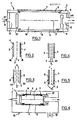
- the device identified as a whole 1, comprises an enclosure 2, into which arrive, by a conduit 8 feed, the reactive gases advantageously opening into the enclosure through an opening located at the front longitudinal end 12 of the enclosure.
- the enclosure 2 which has the general shape of a hollow parallelepiped, is closed towards its front longitudinal end 12 by a first throttle 10 and towards its rear longitudinal end 13 by a second throttle 11.
- the gases being in the enclosure 2 are evacuated at the rear end 13 through the conduit 9.
- the letters "front” and “rear” of the enclosure have been identified by the letters AV and AR, with reference to the circulation of gases in the device as shown by the arrows.
- two film support plates 4 and 5, the substrates are housed in the side walls of the enclosure 2 and arranged substantially parallel to one another.
- the substrates 4 and 5 each have on their rear face, that is to say on the face on which the film generated by the reactive gases will not deposit, a counter electrode 6, 7.
- the enclosure 2 comprises a space 14 formed between the said substrates in which is disposed, substantially centrally, an electrode 3.
- This electrode 3 is in the general form of a substantially flat plate with openwork structure, that is to say in which are formed passages for circulation of the gaseous reaction medium.
- a grid-shaped electrode would be quite suitable.
- the counter electrodes 6 and 7 could also be in the form of a grid.
- the enclosure 2 is arranged in a sealed chamber 15 whose volume is greater than that of the enclosure 2 and in which there is a pressure lower than that of said enclosure.
- Gas under reduced pressure of chamber 15 is evacuated through line 16 in the direction indicated by the arrow.
- the substrates are grounded by means of the counter electrodes 6, 7, and the central electrode 3 receives the electrical power generating the plasma.
- the applied voltage V can be continuous, alternating, even alternating pulsed.
- the distance between the substrates can vary according to the uses but the system retains its major interest only when the spacing between the substrates remains less or of the order of the longitudinal and transverse dimensions of the device.
- the greater the "transparency" or porosity in the reaction medium of the electrode that is to say the larger the spaces provided in its structure, the greater the yield relative to the deposition of material. It should be noted that this transparency of the electrode may however vary depending on the deposit sought and the environment selected. Extreme cases range from the solid plate (which is generally not used in accordance with the invention) to a few wires stretched in the form of a grid, or mesh, on a light frame.
- either the substrates 4 and 5 must be conductive and perform the function of second electrode, either, if the substrates are insulating or if it is desired to avoid the bombardment of the substrate by accelerated particles, three electrodes 3, 23 and 33 are advantageously used in the form of a grid.
- the central electrode 3 is then polarized with respect to the other two 23 and 33, between which a voltage V1 is established, as illustrated in FIG. 3.
- two electrodes designated 3 and 23 can be used, between which a voltage V2 will be established, as illustrated in FIG. 4.
- the other electrode can be provided by the substrates 4 and 5 or if they are insulating by plates or grids, the counter-electrodes 6 and 7 , placed directly on the back side of the substrates.
- the substrates and the film deposits are conductive, it is possible to obtain such bombardment, to polarize them with respect to the other electrode (s). Otherwise, the two counter-electrodes (figure 5) arranged behind the substrates can be connected asymmetrically at the terminals of a radio frequency power source. A voltage V3 is therefore generated and then the plasma-generating discharge on the electrode (s) is supplied, in particular by an alternating generator.
- a wide variety of materials can be deposited in the form of a thin film by decomposition in a chamber under reduced pressure, of one or more reactive gases, diluted or not in one or more carrier gases.
- the deposited semiconductors can be doped by adding, in the gas mixture, a transporter of the doping element.
- the properties of the material generally depend strongly on the chemical purity of the reactant medium and on the ion bombardment (flux, energy) to which the film is subjected during its growth.
- the reactive gases are injected into the enclosure 2 and meet the first throttle 10, also called a distributor, which allows a homogeneous distribution of the gases in the enclosure.
- the gases which are evacuated through the conduit 9 pass into the second throttle 11 to adjust their pressure.
- the evacuation of gases is generally carried out by pumping.
- Leaks of gas from the enclosure to the sealed chamber as well as the degassing of the chamber, the outer walls of the enclosure, the heating systems and other mechanisms present in the chamber, are generally evacuated by a vacuum pump, which is dimensioned to maintain the residual pressure in the chamber at a level much lower than that of the enclosure.
- Figure 6 shows a sealed chamber adapted to the geometry of the enclosure.
- one or more electrodes can be provided in the form of flat perforated plates, the dimensions of the passage orifices of which are adapted as a function of the yield and of the desired deposit.
- FIG. 2 In the operating mode of FIG. 2, only one electrode (3) has been shown. However, one can provide several electrodes, as shown in FIG. 3 or FIG. 4. One can, in particular, with reference to FIG. 4, provide two electrodes (3, 23) of opposite polarity, subjected to an electrical discharge generating plasma and arranged between two substrates (4, 5) connected to ground.
Landscapes
- Chemical & Material Sciences (AREA)
- Engineering & Computer Science (AREA)
- Physics & Mathematics (AREA)
- Plasma & Fusion (AREA)
- Analytical Chemistry (AREA)
- General Chemical & Material Sciences (AREA)
- Chemical Kinetics & Catalysis (AREA)
- Materials Engineering (AREA)
- Mechanical Engineering (AREA)
- Metallurgy (AREA)
- Organic Chemistry (AREA)
- Chemical Vapour Deposition (AREA)
Applications Claiming Priority (2)
| Application Number | Priority Date | Filing Date | Title |
|---|---|---|---|
| FR8515910A FR2589168B1 (fr) | 1985-10-25 | 1985-10-25 | Appareil et son procede d'utilisation pour la formation de films minces assistee par plasma |
| FR8515910 | 1985-10-25 |
Publications (3)
| Publication Number | Publication Date |
|---|---|
| EP0221812A2 true EP0221812A2 (de) | 1987-05-13 |
| EP0221812A3 EP0221812A3 (en) | 1989-03-29 |
| EP0221812B1 EP0221812B1 (de) | 1992-08-26 |
Family
ID=9324220
Family Applications (1)
| Application Number | Title | Priority Date | Filing Date |
|---|---|---|---|
| EP86402312A Expired - Lifetime EP0221812B1 (de) | 1985-10-25 | 1986-10-15 | Vorrichtung und Verfahren zur Herstellung dünner Schichten durch Plasma |
Country Status (5)
| Country | Link |
|---|---|
| US (1) | US4798739A (de) |
| EP (1) | EP0221812B1 (de) |
| JP (1) | JPS62103372A (de) |
| DE (1) | DE3686549T2 (de) |
| FR (1) | FR2589168B1 (de) |
Cited By (6)
| Publication number | Priority date | Publication date | Assignee | Title |
|---|---|---|---|---|
| EP0312447A1 (de) * | 1987-10-15 | 1989-04-19 | SOLEMS S.A. Société dite: | Verfahren und Anlage zur Herstellung dünner Schichten mittels eines Plasmas für elektronische bzw. opto-elektronische Anwendungen |
| DE3739528A1 (de) * | 1987-11-21 | 1989-06-01 | Bbc Brown Boveri & Cie | Cvd-rohrofenreaktor |
| EP0418438A1 (de) * | 1989-09-19 | 1991-03-27 | The University Of Toronto Innovations Foundation | Verfahren und Gerät zum Plasmaätzen, Reinigen von Substraten oder zum Bekleiden mit Stoffen mittels Gleichstrom-Glimmentladung |
| DE4412915B4 (de) * | 1993-05-03 | 2005-12-15 | Unaxis Balzers Ag | Plasmabehandlungsanlage, Verfahren zu deren Betrieb und Verwendung derselben |
| DE4412902B4 (de) * | 1993-05-03 | 2007-02-08 | Oc Oerlikon Balzers Ag | Verfahren zur plasmaunterstützten, chemischen Dampfabscheidung und Vakuumplasmakammer |
| EP1175695A4 (de) * | 1999-08-21 | 2007-04-04 | Lg Electronics Inc | Plasma polymerisationsgeraet mit einer vielzahl von gleichmaesigen randen versehener elektrode |
Families Citing this family (11)
| Publication number | Priority date | Publication date | Assignee | Title |
|---|---|---|---|---|
| FR2677043B1 (fr) * | 1991-05-29 | 1993-12-24 | Solems | Procede, dispositif et appareil pour traiter un substrat par un plasma basse pression. |
| US6296735B1 (en) | 1993-05-03 | 2001-10-02 | Unaxis Balzers Aktiengesellschaft | Plasma treatment apparatus and method for operation same |
| JP3146112B2 (ja) * | 1993-12-24 | 2001-03-12 | シャープ株式会社 | プラズマcvd装置 |
| US5789851A (en) * | 1995-12-15 | 1998-08-04 | Balzers Aktiengesellschaft | Field emission device |
| DE10010016C1 (de) * | 2000-02-26 | 2002-01-31 | Forsch Applikationslabor Plasm | Vorrichtung und Verfahren zur plasmagestützten Oberflächenbehandlung von Substraten im Vakuum |
| JP5027667B2 (ja) | 2004-11-24 | 2012-09-19 | エリコン・ソーラー・アクチェンゲゼルシャフト,トリュープバッハ | 超大面積基板用真空処理チャンバ |
| DE102007022431A1 (de) | 2007-05-09 | 2008-11-13 | Leybold Optics Gmbh | Behandlungssystem für flache Substrate |
| JP5927619B2 (ja) | 2010-05-06 | 2016-06-01 | エヴァテック・アクチェンゲゼルシャフトEvatec Ag | プラズマリアクタ |
| US20130216731A1 (en) * | 2010-09-03 | 2013-08-22 | Tel Solar Ag | Control of differential pressure in pecvd systems |
| EP2654070A1 (de) | 2012-04-16 | 2013-10-23 | INDEOtec SA | Kapazitiv gekoppelter Plasmareaktor für Dünnfilmablagerung |
| KR20140033911A (ko) * | 2012-09-11 | 2014-03-19 | 에이에스엠 아이피 홀딩 비.브이. | 증착 장치 및 증착 방법 |
Family Cites Families (21)
| Publication number | Priority date | Publication date | Assignee | Title |
|---|---|---|---|---|
| US4317844A (en) * | 1975-07-28 | 1982-03-02 | Rca Corporation | Semiconductor device having a body of amorphous silicon and method of making the same |
| JPS533976A (en) * | 1976-06-30 | 1978-01-14 | Nippon Sheet Glass Co Ltd | Process for surface treatment of substrate under vacuum |
| US4226208A (en) * | 1977-08-04 | 1980-10-07 | Canon Kabushiki Kaisha | Vapor deposition apparatus |
| US4123989A (en) * | 1977-09-12 | 1978-11-07 | Mobil Tyco Solar Energy Corp. | Manufacture of silicon on the inside of a tube |
| US4328258A (en) * | 1977-12-05 | 1982-05-04 | Plasma Physics Corp. | Method of forming semiconducting materials and barriers |
| JPS6029295B2 (ja) * | 1979-08-16 | 1985-07-10 | 舜平 山崎 | 非単結晶被膜形成法 |
| DD153497A3 (de) * | 1980-02-08 | 1982-01-13 | Georg Rudakoff | Verfahren und vorrichtung zum plasmaaetzen oder zur plasma cvd |
| US4395323A (en) * | 1981-04-17 | 1983-07-26 | Denton Vacuum Inc. | Apparatus for improving a sputtering process |
| JPS5873111A (ja) * | 1981-10-26 | 1983-05-02 | Seiko Epson Corp | 非晶質半導体膜製造装置 |
| US4423701A (en) * | 1982-03-29 | 1984-01-03 | Energy Conversion Devices, Inc. | Glow discharge deposition apparatus including a non-horizontally disposed cathode |
| JPS58193362A (ja) * | 1982-04-30 | 1983-11-11 | Shimadzu Corp | プラズマcvd装置 |
| CA1184877A (en) * | 1982-05-12 | 1985-04-02 | James B. Webb | Method and apparatus for depositing conducting oxide on a substrate |
| JPS5914633A (ja) * | 1982-07-16 | 1984-01-25 | Anelva Corp | プラズマcvd装置 |
| JPS5935674A (ja) * | 1982-08-24 | 1984-02-27 | Sumitomo Electric Ind Ltd | 蒸着装置 |
| US4545327A (en) * | 1982-08-27 | 1985-10-08 | Anicon, Inc. | Chemical vapor deposition apparatus |
| US4500563A (en) * | 1982-12-15 | 1985-02-19 | Pacific Western Systems, Inc. | Independently variably controlled pulsed R.F. plasma chemical vapor processing |
| JPS59136474A (ja) * | 1983-01-21 | 1984-08-06 | Minolta Camera Co Ltd | 容量結合型グロ−放電分解装置 |
| JPS59193265A (ja) * | 1983-03-14 | 1984-11-01 | Stanley Electric Co Ltd | プラズマcvd装置 |
| EP0135294A3 (de) * | 1983-07-18 | 1986-08-20 | Energy Conversion Devices, Inc. | Legierungen niedrigen Bandabstandes für fotovoltaische Anwendungen |
| JPS6063370A (ja) * | 1983-09-16 | 1985-04-11 | Hitachi Koki Co Ltd | アモルファス水素化シリコン膜製造装置 |
| JPS6164877A (ja) * | 1984-09-07 | 1986-04-03 | Hitachi Ltd | 薄膜成膜装置 |
-
1985
- 1985-10-25 FR FR8515910A patent/FR2589168B1/fr not_active Expired - Lifetime
-
1986
- 1986-10-15 DE DE8686402312T patent/DE3686549T2/de not_active Expired - Lifetime
- 1986-10-15 EP EP86402312A patent/EP0221812B1/de not_active Expired - Lifetime
- 1986-10-21 US US06/921,072 patent/US4798739A/en not_active Expired - Lifetime
- 1986-10-24 JP JP61253502A patent/JPS62103372A/ja active Granted
Cited By (8)
| Publication number | Priority date | Publication date | Assignee | Title |
|---|---|---|---|---|
| EP0312447A1 (de) * | 1987-10-15 | 1989-04-19 | SOLEMS S.A. Société dite: | Verfahren und Anlage zur Herstellung dünner Schichten mittels eines Plasmas für elektronische bzw. opto-elektronische Anwendungen |
| FR2621930A1 (fr) * | 1987-10-15 | 1989-04-21 | Solems Sa | Procede et appareil pour la production par plasma de couches minces a usage electronique et/ou optoelectronique |
| DE3739528A1 (de) * | 1987-11-21 | 1989-06-01 | Bbc Brown Boveri & Cie | Cvd-rohrofenreaktor |
| EP0418438A1 (de) * | 1989-09-19 | 1991-03-27 | The University Of Toronto Innovations Foundation | Verfahren und Gerät zum Plasmaätzen, Reinigen von Substraten oder zum Bekleiden mit Stoffen mittels Gleichstrom-Glimmentladung |
| DE4412915B4 (de) * | 1993-05-03 | 2005-12-15 | Unaxis Balzers Ag | Plasmabehandlungsanlage, Verfahren zu deren Betrieb und Verwendung derselben |
| DE4412902B4 (de) * | 1993-05-03 | 2007-02-08 | Oc Oerlikon Balzers Ag | Verfahren zur plasmaunterstützten, chemischen Dampfabscheidung und Vakuumplasmakammer |
| DE4447977B4 (de) * | 1993-05-03 | 2009-09-10 | Oc Oerlikon Balzers Ag | Vorrichtung und Verfahren zur Plasmabehandlung von flachen Werkstücken, insbesondere flachen, aktiven Bildschirmen, sowie Verwendung der Vorrichtung |
| EP1175695A4 (de) * | 1999-08-21 | 2007-04-04 | Lg Electronics Inc | Plasma polymerisationsgeraet mit einer vielzahl von gleichmaesigen randen versehener elektrode |
Also Published As
| Publication number | Publication date |
|---|---|
| FR2589168A1 (fr) | 1987-04-30 |
| FR2589168B1 (fr) | 1992-07-17 |
| DE3686549T2 (de) | 1993-03-11 |
| EP0221812A3 (en) | 1989-03-29 |
| JPS62103372A (ja) | 1987-05-13 |
| US4798739A (en) | 1989-01-17 |
| JPH0541705B2 (de) | 1993-06-24 |
| EP0221812B1 (de) | 1992-08-26 |
| DE3686549D1 (de) | 1992-10-01 |
Similar Documents
| Publication | Publication Date | Title |
|---|---|---|
| EP0221812B1 (de) | Vorrichtung und Verfahren zur Herstellung dünner Schichten durch Plasma | |
| JP5350261B2 (ja) | プラズマからの非晶質材料の蒸着による勾配付きバンドギャップを有する膜の形成方法 | |
| EP0200651B1 (de) | Dreielektrodenionenquelle mit einer einzigen Hochfrequenzionisationskammer und mit multipolarer magnetischer Umschliessung | |
| EP0424256B1 (de) | Gerät für chemische Behandlung mit Hilfe eines Diffusionsplasmas | |
| EP0359777A1 (de) | Ätzverfahren mittels gasplasma. | |
| EP0871979A1 (de) | Verfahren und vorrichtung zur abscheidung mindestens einer eigenleitenden hydrierten mikrokristallinen oder nanokristallinen siliziumschicht und so hergestellte solarzelle | |
| CH668145A5 (fr) | Procede et installation de depot de silicium amorphe hydrogene sur un substrat dans une enceinte a plasma. | |
| EP0129490A1 (de) | Verfahren und Einrichtung zum Erzeugen eines homogenen Plasmas mit einem grossen Volumen, einer hohen Dichte und einer niedrigen Elektronentemperatur | |
| WO2003083893A1 (fr) | Dispositif de confinement d'un plasma dans un volume | |
| FR2691035A1 (fr) | Dispositif et machine à plasma de traitement chimique et procédé utilisant ce dispositif. | |
| EP1518256B1 (de) | Verfahren zur erzeugung eines grossflächigen plasmas | |
| EP0346168B1 (de) | Plasmareaktor | |
| FR2600269A1 (fr) | Procede et agencement pour pulveriser une matiere par decharge a haute frequence | |
| EP2338318B1 (de) | Niederleistungs-gasplasmaquelle | |
| EP0995345A1 (de) | Vorrichtung zur anregung eines gases durch oberflächenwellenplasma | |
| FR2677043A1 (fr) | Procede, dispositif et appareil pour traiter un substrat par un plasma basse pression. | |
| US4799968A (en) | Photovoltaic device | |
| EP1094494A1 (de) | Verfahren zur Plasmaerzeugung durch kapazitive mehrpolig-behinderte Entladung und Implementierungsvorrichtung dafür | |
| WO2020229529A1 (fr) | Dispositif de depôt chimique en phase vapeur presentant des zones de depôt reconfigurables | |
| FR2689143A1 (fr) | Dispositif de pulvérisation cathodique utilisant un plasma engendré par des micro-ondes. | |
| JP2846534B2 (ja) | プラズマcvd装置とこれによる機能性堆積膜の形成方法 | |
| EP1094691B1 (de) | Verfahren zur Plasmaerzeugung durch kapazitive gleichmässige Entladungen und Implementierungsvorrichtung dafür | |
| WO2003049139A1 (fr) | Source d'electrons | |
| EP0300932B1 (de) | ELektronenquelle | |
| BE1026449B1 (fr) | Procédé et dispositif de synthèse de diamant par CVD |
Legal Events
| Date | Code | Title | Description |
|---|---|---|---|
| PUAI | Public reference made under article 153(3) epc to a published international application that has entered the european phase |
Free format text: ORIGINAL CODE: 0009012 |
|
| AK | Designated contracting states |
Kind code of ref document: A2 Designated state(s): BE CH DE GB IT LI LU NL SE |
|
| 111L | Licence recorded |
Free format text: 0100 NEXTRAL S.A. |
|
| PUAL | Search report despatched |
Free format text: ORIGINAL CODE: 0009013 |
|
| AK | Designated contracting states |
Kind code of ref document: A3 Designated state(s): BE CH DE GB IT LI LU NL SE |
|
| 17P | Request for examination filed |
Effective date: 19890619 |
|
| 17Q | First examination report despatched |
Effective date: 19890928 |
|
| GRAA | (expected) grant |
Free format text: ORIGINAL CODE: 0009210 |
|
| AK | Designated contracting states |
Kind code of ref document: B1 Designated state(s): BE CH DE GB IT LI LU NL SE |
|
| PG25 | Lapsed in a contracting state [announced via postgrant information from national office to epo] |
Ref country code: SE Free format text: THE PATENT HAS BEEN ANNULLED BY A DECISION OF A NATIONAL AUTHORITY Effective date: 19920826 Ref country code: NL Effective date: 19920826 Ref country code: IT Free format text: LAPSE BECAUSE OF FAILURE TO SUBMIT A TRANSLATION OF THE DESCRIPTION OR TO PAY THE FEE WITHIN THE PRE;WARNING: LAPSES OF ITALIAN PATENTS WITH EFFECTIVE DATE BEFORE 2007 MAY HAVE OCCURRED AT ANY TIME BEFORE 2007. THE CORRECT EFFECTIVE DATE MAY BE DIFFERENT FROM THE ONE RECORDED.SCRIBED TIME-LIMIT Effective date: 19920826 |
|
| REF | Corresponds to: |
Ref document number: 3686549 Country of ref document: DE Date of ref document: 19921001 |
|
| REG | Reference to a national code |
Ref country code: CH Ref legal event code: PLI Owner name: NEXTRAL S.A. |
|
| PG25 | Lapsed in a contracting state [announced via postgrant information from national office to epo] |
Ref country code: BE Effective date: 19921031 Ref country code: LU Free format text: LAPSE BECAUSE OF NON-PAYMENT OF DUE FEES Effective date: 19921031 |
|
| GBT | Gb: translation of ep patent filed (gb section 77(6)(a)/1977) | ||
| NLV1 | Nl: lapsed or annulled due to failure to fulfill the requirements of art. 29p and 29m of the patents act | ||
| BERE | Be: lapsed |
Owner name: S.A. SOLEMS Effective date: 19921031 |
|
| PLBE | No opposition filed within time limit |
Free format text: ORIGINAL CODE: 0009261 |
|
| STAA | Information on the status of an ep patent application or granted ep patent |
Free format text: STATUS: NO OPPOSITION FILED WITHIN TIME LIMIT |
|
| 26N | No opposition filed | ||
| REG | Reference to a national code |
Ref country code: GB Ref legal event code: IF02 |
|
| PGFP | Annual fee paid to national office [announced via postgrant information from national office to epo] |
Ref country code: GB Payment date: 20051012 Year of fee payment: 20 |
|
| PGFP | Annual fee paid to national office [announced via postgrant information from national office to epo] |
Ref country code: DE Payment date: 20051014 Year of fee payment: 20 |
|
| REG | Reference to a national code |
Ref country code: GB Ref legal event code: PE20 |
|
| PGFP | Annual fee paid to national office [announced via postgrant information from national office to epo] |
Ref country code: CH Payment date: 20060123 Year of fee payment: 20 |
|
| PG25 | Lapsed in a contracting state [announced via postgrant information from national office to epo] |
Ref country code: GB Free format text: LAPSE BECAUSE OF EXPIRATION OF PROTECTION Effective date: 20061014 |
|
| REG | Reference to a national code |
Ref country code: CH Ref legal event code: PL |