EP0222668B1 - Procédé de fabrication par gravure en escalier d'un transistor en couches minces à grille auto-alignée par rapport au drain et à la source de celui-ci et transistor obtenu par ce procédé - Google Patents
Procédé de fabrication par gravure en escalier d'un transistor en couches minces à grille auto-alignée par rapport au drain et à la source de celui-ci et transistor obtenu par ce procédé Download PDFInfo
- Publication number
- EP0222668B1 EP0222668B1 EP86402497A EP86402497A EP0222668B1 EP 0222668 B1 EP0222668 B1 EP 0222668B1 EP 86402497 A EP86402497 A EP 86402497A EP 86402497 A EP86402497 A EP 86402497A EP 0222668 B1 EP0222668 B1 EP 0222668B1
- Authority
- EP
- European Patent Office
- Prior art keywords
- layer
- etching
- transistor
- resin
- gate
- Prior art date
- Legal status (The legal status is an assumption and is not a legal conclusion. Google has not performed a legal analysis and makes no representation as to the accuracy of the status listed.)
- Expired - Lifetime
Links
- 238000005530 etching Methods 0.000 title claims description 36
- 238000000034 method Methods 0.000 title claims description 21
- 239000010409 thin film Substances 0.000 title claims description 9
- 229920005989 resin Polymers 0.000 claims description 32
- 239000011347 resin Substances 0.000 claims description 32
- 229910052710 silicon Inorganic materials 0.000 claims description 28
- 239000010703 silicon Substances 0.000 claims description 28
- XUIMIQQOPSSXEZ-UHFFFAOYSA-N Silicon Chemical compound [Si] XUIMIQQOPSSXEZ-UHFFFAOYSA-N 0.000 claims description 26
- 239000000758 substrate Substances 0.000 claims description 10
- 229910021417 amorphous silicon Inorganic materials 0.000 claims description 9
- 230000008021 deposition Effects 0.000 claims description 6
- 239000011521 glass Substances 0.000 claims description 3
- 230000008030 elimination Effects 0.000 claims 2
- 238000003379 elimination reaction Methods 0.000 claims 2
- 238000004519 manufacturing process Methods 0.000 description 11
- 239000000463 material Substances 0.000 description 7
- 238000000151 deposition Methods 0.000 description 5
- VYZAMTAEIAYCRO-UHFFFAOYSA-N Chromium Chemical compound [Cr] VYZAMTAEIAYCRO-UHFFFAOYSA-N 0.000 description 2
- 229910018503 SF6 Inorganic materials 0.000 description 2
- 229910052804 chromium Inorganic materials 0.000 description 2
- 239000011651 chromium Substances 0.000 description 2
- 238000001312 dry etching Methods 0.000 description 2
- 239000004973 liquid crystal related substance Substances 0.000 description 2
- 230000000873 masking effect Effects 0.000 description 2
- 239000011159 matrix material Substances 0.000 description 2
- 238000000206 photolithography Methods 0.000 description 2
- 239000004065 semiconductor Substances 0.000 description 2
- 150000003376 silicon Chemical class 0.000 description 2
- SFZCNBIFKDRMGX-UHFFFAOYSA-N sulfur hexafluoride Chemical compound FS(F)(F)(F)(F)F SFZCNBIFKDRMGX-UHFFFAOYSA-N 0.000 description 2
- 229960000909 sulfur hexafluoride Drugs 0.000 description 2
- VYPSYNLAJGMNEJ-UHFFFAOYSA-N Silicium dioxide Chemical compound O=[Si]=O VYPSYNLAJGMNEJ-UHFFFAOYSA-N 0.000 description 1
- QVGXLLKOCUKJST-UHFFFAOYSA-N atomic oxygen Chemical compound [O] QVGXLLKOCUKJST-UHFFFAOYSA-N 0.000 description 1
- 239000003990 capacitor Substances 0.000 description 1
- 238000005119 centrifugation Methods 0.000 description 1
- 238000005229 chemical vapour deposition Methods 0.000 description 1
- 238000007796 conventional method Methods 0.000 description 1
- 230000005669 field effect Effects 0.000 description 1
- SLGWESQGEUXWJQ-UHFFFAOYSA-N formaldehyde;phenol Chemical compound O=C.OC1=CC=CC=C1 SLGWESQGEUXWJQ-UHFFFAOYSA-N 0.000 description 1
- 230000006870 function Effects 0.000 description 1
- 239000007789 gas Substances 0.000 description 1
- 239000008246 gaseous mixture Substances 0.000 description 1
- 229910021421 monocrystalline silicon Inorganic materials 0.000 description 1
- 230000005693 optoelectronics Effects 0.000 description 1
- 229910052760 oxygen Inorganic materials 0.000 description 1
- 239000001301 oxygen Substances 0.000 description 1
- 229920001568 phenolic resin Polymers 0.000 description 1
- 238000001259 photo etching Methods 0.000 description 1
- 229910052814 silicon oxide Inorganic materials 0.000 description 1
- 238000005507 spraying Methods 0.000 description 1
- 239000000126 substance Substances 0.000 description 1
- 238000007738 vacuum evaporation Methods 0.000 description 1
Images

Classifications
-
- H—ELECTRICITY
- H10—SEMICONDUCTOR DEVICES; ELECTRIC SOLID-STATE DEVICES NOT OTHERWISE PROVIDED FOR
- H10D—INORGANIC ELECTRIC SEMICONDUCTOR DEVICES
- H10D30/00—Field-effect transistors [FET]
- H10D30/01—Manufacture or treatment
- H10D30/021—Manufacture or treatment of FETs having insulated gates [IGFET]
- H10D30/031—Manufacture or treatment of FETs having insulated gates [IGFET] of thin-film transistors [TFT]
- H10D30/0312—Manufacture or treatment of FETs having insulated gates [IGFET] of thin-film transistors [TFT] characterised by the gate electrodes
- H10D30/0316—Manufacture or treatment of FETs having insulated gates [IGFET] of thin-film transistors [TFT] characterised by the gate electrodes of lateral bottom-gate TFTs comprising only a single gate
-
- H—ELECTRICITY
- H10—SEMICONDUCTOR DEVICES; ELECTRIC SOLID-STATE DEVICES NOT OTHERWISE PROVIDED FOR
- H10D—INORGANIC ELECTRIC SEMICONDUCTOR DEVICES
- H10D30/00—Field-effect transistors [FET]
- H10D30/01—Manufacture or treatment
- H10D30/021—Manufacture or treatment of FETs having insulated gates [IGFET]
- H10D30/031—Manufacture or treatment of FETs having insulated gates [IGFET] of thin-film transistors [TFT]
- H10D30/0321—Manufacture or treatment of FETs having insulated gates [IGFET] of thin-film transistors [TFT] comprising silicon, e.g. amorphous silicon or polysilicon
-
- H—ELECTRICITY
- H10—SEMICONDUCTOR DEVICES; ELECTRIC SOLID-STATE DEVICES NOT OTHERWISE PROVIDED FOR
- H10D—INORGANIC ELECTRIC SEMICONDUCTOR DEVICES
- H10D30/00—Field-effect transistors [FET]
- H10D30/60—Insulated-gate field-effect transistors [IGFET]
- H10D30/67—Thin-film transistors [TFT]
- H10D30/6729—Thin-film transistors [TFT] characterised by the electrodes
- H10D30/673—Thin-film transistors [TFT] characterised by the electrodes characterised by the shapes, relative sizes or dispositions of the gate electrodes
- H10D30/6732—Bottom-gate only TFTs
-
- H—ELECTRICITY
- H10—SEMICONDUCTOR DEVICES; ELECTRIC SOLID-STATE DEVICES NOT OTHERWISE PROVIDED FOR
- H10D—INORGANIC ELECTRIC SEMICONDUCTOR DEVICES
- H10D30/00—Field-effect transistors [FET]
- H10D30/60—Insulated-gate field-effect transistors [IGFET]
- H10D30/67—Thin-film transistors [TFT]
- H10D30/674—Thin-film transistors [TFT] characterised by the active materials
- H10D30/6741—Group IV materials, e.g. germanium or silicon carbide
- H10D30/6743—Silicon
- H10D30/6746—Amorphous silicon
-
- Y—GENERAL TAGGING OF NEW TECHNOLOGICAL DEVELOPMENTS; GENERAL TAGGING OF CROSS-SECTIONAL TECHNOLOGIES SPANNING OVER SEVERAL SECTIONS OF THE IPC; TECHNICAL SUBJECTS COVERED BY FORMER USPC CROSS-REFERENCE ART COLLECTIONS [XRACs] AND DIGESTS
- Y10—TECHNICAL SUBJECTS COVERED BY FORMER USPC
- Y10S—TECHNICAL SUBJECTS COVERED BY FORMER USPC CROSS-REFERENCE ART COLLECTIONS [XRACs] AND DIGESTS
- Y10S438/00—Semiconductor device manufacturing: process
- Y10S438/942—Masking
- Y10S438/948—Radiation resist
- Y10S438/949—Energy beam treating radiation resist on semiconductor
-
- Y—GENERAL TAGGING OF NEW TECHNOLOGICAL DEVELOPMENTS; GENERAL TAGGING OF CROSS-SECTIONAL TECHNOLOGIES SPANNING OVER SEVERAL SECTIONS OF THE IPC; TECHNICAL SUBJECTS COVERED BY FORMER USPC CROSS-REFERENCE ART COLLECTIONS [XRACs] AND DIGESTS
- Y10—TECHNICAL SUBJECTS COVERED BY FORMER USPC
- Y10S—TECHNICAL SUBJECTS COVERED BY FORMER USPC CROSS-REFERENCE ART COLLECTIONS [XRACs] AND DIGESTS
- Y10S438/00—Semiconductor device manufacturing: process
- Y10S438/978—Semiconductor device manufacturing: process forming tapered edges on substrate or adjacent layers
Definitions
- the present invention relates to a method of manufacturing by etching a thin film transistor with a self-aligned gate with respect to the drain and the source thereof and the transistor obtained by this method.
- TCM thin film transistors
- This electronic memory which stores the video signal throughout the duration of the image is produced, in the form of an active matrix, of memory points each consisting of a TCM and a capacitor and distributed over the entire surface of the screen.
- the liquid crystal is in contact with each memory point and is excited for the duration of an image.
- a thin film transistor is an insulated gate field effect transistor. It is similar to the MOS (metal-oxide-semiconductor) transistor with the difference that it is produced on an amorphous substrate and not on a monocrystalline silicon wafer. Therefore, as they are no longer limited by the size of the crystalline substrate, the TCM circuits can then have very large dimensions.
- MOS metal-oxide-semiconductor
- Patent publication FR-A-2 553 579 discloses a method for manufacturing a thin-film transistor making it possible in particular to align the gate of the transistor with the drain and the source thereof.
- the sides of the first layer of silicon, after the photo-etching thereof, are vertical and do not therefore offer a good contact and bonding surface for the deposition of a second layer of n + type silicon in order to make ohmic contacts.
- the object of the invention is precisely to improve the contact surface of the sides of a layer of a material of a mainly conductive or semi-conductive nature, by staircase etching so that the deposition of another layer d 'A material of a mainly conductive or semi-conductive nature is better, especially with a view to making ohmic contacts.
- This object is achieved, according to the invention, by the production of a certain number of stair treads, on the sides of the layer of the material by an equal number of successive and partial engravings of this layer, the remaining resin serving to each time mask and is itself etched isotropically over a small thickness after each etching of the layer of material.
- a person skilled in the art designates the fact of selectively removing, by chemical attack, a layer thickness of a material.
- a layer of photosensitive resin acts as a mask during said etching in order to obtain the desired shape of the layer.
- the subject of the invention is a method for manufacturing a thin film transistor, with a gate self-aligned with respect to the drain and the source thereof, according to claim 1.
- the present invention also relates to a thin film transistor with a self-aligned gate, according to claim 2.
- the stair treads obtained on the sides of the first silicon layer have a length equal to the thickness of the resin removed by an isotropic etching taking place at the end of each etching of this silicon layer.
- obtaining the stair treads is carried out on the same layer of material. This uniqueness promotes the implementation of the process and does not generate a critical step.
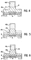
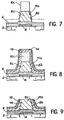
- FIGS. 1 to 9 illustrate the different stages of the method according to the invention.
- the first step of the method consists in producing, on a glass substrate 2, the gate 4 of the transistor using the conventional methods of photolithography (masking and etching).
- This grid 4, for example having a thickness of 100 nm is preferably made of chromium.
- an insulating layer preferably made of silicon oxide, is deposited on the substrate 2 and the gate 4 of the transistor.
- This insulating layer 6 having for example a thickness of 100 nm can be obtained by the chemical vapor deposition technique, at low pressure or not, or else by the glow discharge technique, in a radiofrequency device, using a gaseous mixture of SiH 4 and 0 2 .
- a first layer of thick hydrogenated amorphous silicon 8 advantageously having a thickness varying from 70 to 100 nm or close to 80 nm.
- This silicon layer can be obtained by the glow discharge technique using the gas SiH 4 .
- the next step of the process consists in depositing, on the thick amorphous silicon layer 8, a layer of positive photosensitive resin 10.
- This resin layer can advantageously have a thickness varying from 1,000 to 1,200 nm and can in particular be deposited by centrifugation.
- resin resins based on phenolformaldehyde such as that sold by the company Hunt under the reference HPR 204 can be used.
- the photosensitive resin layer 10 is then irradiated through the substrate 2, the grid 4 then serving as a mask for the irradiation.
- the use of a sensitive resin in the visible makes it possible to reduce the duration of this irradiation (the arrows shown in FIG. 2 indicate the direction of the irradiation).
- the next step, characteristic of the invention is the particular etching of the first layer of silicon 8 which makes it possible to produce a certain number of stair treads on the sides of this layer of silicon.
- the various operations carried out during this particular etching are represented in FIGS. 3 to 7 by dotted lines which thus make it possible to follow the progress of the process.
- the resin 10a is annealed at a temperature between 100 and 150 ° C. and preferably close to 130 ° C., to obtain a creep. of it.
- the etching used is a dry etching, using a sulfur hexafluoride plasma.
- the partial etching is at least equal to one third of the thickness of the initial hydrogenated amorphous silicon layer.
- the process which is the subject of the invention then consists in etching isotropically, a small thickness of resin.
- the etching shows on the top of the sides of the silicon layer 8a, a first step 9 of width equal to that of the etched resin layer.
- the etching used is a dry, ionic and reactive etching and the remaining resin 10b has a thickness of the order of 150 nm less than that of the initial resin 10a in FIG. 3.
- the etching of part of the thickness of the silicon layer is renewed, the remaining resin 10b serving as a mask for said etching.
- This second partial etching similarly attacks the step 9 and reveals a first step 9a on the flanks of the remaining silicon layer 8b.
- the isotropic etching is renewed in an identical manner, with a small thickness of resin 10b, which etching revealing a second step 11 on the top of the flanks of the silicon layer 8b, of the same length as the thickness of the etched resin layer.
- the etching operation of the silicon layer is repeated until the insulating layer 6 is exposed, the remaining resin 10c serving as a mask for said etching.
- This last partial etching similarly attacks the step 11 and the step 9a (FIG. 6) and reveals a second step 11 a which is added to the first step 9b on the sides of the remaining silicon layer 8c (Fig. .7).
- etchings produced in the silicon layer on the one hand and in the resin on the other hand be carried out respectively according to identical methods.
- dry etching using a sulfur hexafluoride plasma for the silicon layer, and an oxygen plasma for the resin.
- the fabrication of the transistor is completed by depositing, in a known manner over the entire structure, a second layer of amorphous silicon 12 of n + type, hydrogenated or not, having for example a thickness of 20 nm.
- This second silicon layer 12 deposited by the same technique as that used for the first silicon layer, allows the production of ohmic contacts for the source and the drain of the transistor.
- This layer 12 is then covered with a conductive layer 14 preferably made of chromium.
- This conductive layer 14 having for example a thickness of 150 nm, is obtained by deposition, for example by vacuum evaporation or by spraying.
- the electrodes of the source, drain of the transistor are produced by the conventional photolithography methods (masking and etching).
Landscapes
- Thin Film Transistor (AREA)
- Drying Of Semiconductors (AREA)
Description
- La présente invention a pour objet un procédé de fabrication par gravure d'un transistor en couches minces à grille auto-alignée par rapport au drain et à la source de celui-ci et le transistor obtenu par ce procédé.
- D'une façon générale, elle permet la fabrication des composants semi-conducteurs en couches minces pouvant servir au multiplexage de tels composants disposés sous forme matricielle, ainsi qu'à la réalisation de dispositifs à transfert de charge (DTC) ou (CCD charge coupled device en terminologie anglo-saxonne).
- Plus particulièrement, elle permet la fabrication de transistors en couches minces (TCM en abrégé) pouvant servir en optoélectronique à la réalisation de la mémoire électronique des écrans plats à cristaux liquides. Cette mémoire électronique qui stocke le signal vidéo pendant toute la durée de l'image est réalisée, sous forme de matrice active, de points mémoires constitués chacun d'un TCM et d'un condensateur et répartis sur toute la surface de l'écran. Le cristal liquide est en contact avec chaque point mémoire et est excité pendant toute la durée d'une image.
- Un transistor en couches minces est un transistor à effet de champ à grille isolée. Il s'apparente au transistor MOS (métal-oxyde-semiconducteur) avec cette différence qu'il est réalisé sur un substrat amorphe et non sur une plaquette de silicium mo- nocristallin. De ce fait, comme ils ne sont plus limités par la taille du substrat cristallin, les circuits à TCM peuvent alors présenter de très grandes dimensions.
- On connaît par la publication de brevet FR-A-2 553 579 un procédé de fabrication de transistor en couches minces permettant notamment d'aligner la grille du transistor avec le drain et la source de celui-ci. Malheureusement, les flancs de la première couche de silicium, après la photogravure de celle-ci, sont verticaux et n'offrent pas ainsi une bonne surface de contact et d'accrochage pour le dépôt d'une seconde couche de silicium de type n+ en vue de réaliser des contacts ohmiques.
- Le but de l'invention est précisément d'améliorer la surface de contact des flancs d'une couche d'un matériau de nature principalement conductrice ou semi-conductrice, par gravure en escalier de telle sorte que le dépôt d'une autre couche d'un matériau de nature principalement conductrice ou semi-conductrice soit meilleur, notamment en vue de réaliser des contacts ohmiques.
- Ce but est atteint, selon l'invention, par la réalisation d'un certain nombre de marches d'escalier, sur les flancs de la couche du matériau par un nombre égal de gravures successives et partielles de cette couche, la résine restante servant à chaque fois de masque et étant elle-même gravée de façon isotrope sur une faible épaisseur à l'issue de chaque gravure de la couche du matériau.
- Par gravure, l'homme du métier désigne le fait d'ôter de façon sélective par attaque chimique, une épaisseur de couche d'un matériau. Généralement, une couche de résine photosensible joue le rôle de masque à ladite gravure afin d'obtenir la forme souhaitée de la couche.
- De façon plus précise, l'invention a pour objet un procédé de fabrication d'un transistor en couches minces, à grille auto-alignée par rapport au drain et à la source de celui-ci, conforme à la revendication 1.
- La présente invention a également pour objet un transistor en couches minces à grille auto-alignée, conforme à la revendication 2.
- Il est possible, selon l'invention, d'obtenir une surface de contact dont .la qualité est fonction du nombre et de la forme des marches que l'on peut réaliser sur les flancs de la couche.
- Les limites de cette réalisation sont définies essentiellement par la technique de gravure employée et les épaisseurs des couches du matériau et de la résine présentes. Ce résultat est obtenu grâce à la gravure de la première couche de silicium qui constitue l'étape essentielle et nouvelle de l'invention par rapport à l'enseignement du document FR-A-2 553 579.
- Les marches d'escalier obtenues sur les flancs de la première couche de silicium ont une longueur égale à l'épaisseur de la résine enlevée par une gravure isotrope ayant lieu à l'issue de chaque gravure de cette couche de silicium.
- On note également que l'obtention des marches d'escalier est réalisée sur la même couche de matériau. Cette unicité favorise la mise en oeuvre du procédé et n'engendre pas d'étape critique.
- Les caractéristiques de l'invention apparaîtront mieux après la description qui suit, d'un exemple de réalisation donné à titre explicatif et nullement limitatif, en référence aux figures 1 à 9 annexées, qui illustrent les différentes étapes du procédé selon l'invention.
- Comme représenté sur la figure 1, la première étape du procédé consiste à réaliser, sur un substrat en verre 2, la grille 4 du transistor en utilisant les procédés classiques de la photolithographie (masquage et gravure). Cette grille 4, présentant par exemple une épaisseur de 100 nm est réalisée de préférence en chrome.
- On dépose ensuite, sur le substrat 2 et la grille 4 du transistor, une couche d'isolant, réalisée de préférence en oxyde de silicium. Cette couche d'isolant 6 présentant par exemple une épaisseur de 100 nm peut être obtenue par la technique de dépôt chimique en phase vapeur, à basse pression ou non, ou bien par la technique de décharge luminescente, dans un appareil à radiofréquence, en utilisant un mélange gazeux de SiH4 et de 02.
- On dépose ensuite, sur la couche d'isolant 6, une première couche de silicium amorphe hydrogéné 8 épaisse, présentant avantageusement une épaisseur variant de 70 à 100 nm ou voisine de 80 nm.
- Cette couche de silicium peut être obtenue par la technique de décharge luminescente en utilisant le gaz SiH4.
- L'étape suivante du procédé consiste à déposer, sur la couche de silicium amorphe épaisse 8, une couche de résine photosensible positive 10.
- Cette couche de résine peut présenter avantageusement une épaisseur variant de 1 000 à 1 200 nm et peut être notamment déposée par centrifugation. Comme résine, on peut utiliser des résines à base de phénolformaldéhyde comme celle vendue par la société HUNT sous la référence HPR 204.
- Comme représenté par la figure 2, la couche de résine photosensible 10 est ensuite irradiée à travers le substrat 2, la grille 4 servant alors de masque à l'irradiation. L'utilisation d'une résine sensible dans le visible permet de diminuer la durée de cette irradiation (les flèches portées sur la figure 2 indiquent le sens de l'irradiation).
- Le développement de la couche de résine permet de ne garder de cette couche que la zone 10a située au droit de la grille du transistor, les zones irradiées étant éliminées.
- L'étape suivante, caractéristique de l'invention est la gravure particulière de la première couche de silicium 8 qui permet de réaliser un certain nombre de marches d'escalier sur les flancs de cette couche de silicium. Les différentes opérations réalisées lors de cette gravure particulière, sont représentées sur les figures 3 à 7 par des pointillés qui permettent ainsi de suivre l'évolution du procédé. Comme représenté sur la figure 3, on procède tout d'abord pendant une durée voisine de 30 minutes, au recuit de la résine 10a à une température comprise entre 100 et 150°C et de préférence voisine de 130°C, pour obtenir un fluage de celle-ci.
- Ensuite, on grave une partie de l'épaisseur de la couche de silicium amorphe hydrogéné 8, la résine restante 10a servant de masque ladite gravure. Il subsiste, après cette première gravure partielle, une couche de silicium 8a.
- De préférence, la gravure employée est une gravure sèche, utilisant un plasma d'hexafluorure de soufre. De préférence, la gravure partielle est au minimum égale au tiers de l'épaisseur de la couche de silicium amorphe hydrogéné initiale.
- Comme représenté sur la figure 4, le procédé objet de l'invention consiste ensuite à graver de façon isotrope, une faible épaisseur de résine. La gravure fait apparaître sur le sommet des flancs de la couche de silicium 8a, un premier décrochement 9 de largeur égale à celle de la couche de résine gravée.
- De préférence, la gravure employée est une gravure sèche, ionique et réactive et la résine restante 10b a une épaisseur inférieure de l'ordre de 150 nm par rapport à celle de la résine initiale 10a de la figure 3.
- Comme représenté sur la figure 5, on renouvelle la gravure d'une partie de l'épaisseur de la couche de silicium, la résine restante 10b servant de masque à ladite gravure. Cette seconde gravure partielle attaque de la même façon le décrochement 9 et fait apparaître une première marche 9a sur les flancs de la couche de silicium restante 8b.
- Comme représenté sur la figure 6, on renouvelle, de façon identique la gravure isotrope, d'une faible épaisseur de résine 10b, laquelle gravure faisant apparaître un second décrochement 11 sur le sommet des flancs de la couche de silicium 8b, de même longueur que l'épaisseur de la couche de résine gravée.
- Comme représenté sur la figure 7, l'opération de gravure de la couche de silicium est renouvelée jusqu'à mise à nu de la couche d'isolant 6, la résine restante 10c servant de masque à ladite gravure. Cette dernière gravure partielle attaque de la même façon le décrochement 11 et la marche 9a (Fig.6) et fait apparaître une seconde marche 11 a qui s'ajoute à la première marche 9b sur les flancs de la couche de silicium restante 8c (Fig.7).
- Dans l'exemple de mise en oeuvre décrit en se référant aux figures 3 à 7, on a réalisé dans la couche de silicium deux marches successives. Il doit être bien entendu que ceci est un exemple préférentiel mais non limitatif et que l'on pourrait tout aussi bien, sans sortir du cadre de l'invention, étendre le procédé à la réalisation d'un nombre de marches supérieur à deux.
- Dans tous les cas, il est préférable pour des raisons de simplicité de mise en oeuvre technologique, que toutes les gravures réalisées dans la couche de silicium d'une part et dans la résine d'autre part, soient effectuées repectivement selon des méthodes identiques. (De préférence gravure sèche, en utilisant un plasma d'hexafluorure de soufre pour la couche de silicium, et un plasma d'oxygène pour la résine).
- Comme représenté sur la figure 8, on parachève la fabrication de transistor en déposant de façon connue sur l'ensemble de la structure, une seconde couche de silicium amorphe 12 de type n+ hydrogéné ou non, présentant par exemple une épaisseur de 20 nm. Cette seconde couche de silicium 12, déposée par la même technique que celle utilisée pour la première couche de silicium, permet la réalisation de contacts ohmiques pour la source et le drain du transistor. Cette couche 12 est ensuite recouverte d'une couche conductrice 14 réalisée de préférence en chrome. Cette couche conductrice 14 présentant par exemple une épaisseur de 150 nm, est obtenue par dépôt, par exemple par évaporation sous vide ou par pulvérisation.
- Comme représenté sur la figure 9, au moyen de la technique connue sous l'expression anglo-saxonne "lift off", on élimine les régions respectivement de la couche conductrice 14 et de la seconde couche de silicium 12, situées au droit de la grille 4 du transistor et la résine restante 10c.
- On réalise enfin, dans ce qui reste de la couche conductrice 14, les électrodes de la source, drain du transistor par les procédés classiques de photolithographie (masquage et gravure).
Claims (2)
caractérisé par le fait que les premières couches de silicium amorphe hydrogéné (8) présentent des flancs en escalier constitués d'au moins deux marches.
Applications Claiming Priority (2)
| Application Number | Priority Date | Filing Date | Title |
|---|---|---|---|
| FR8516922A FR2590409B1 (fr) | 1985-11-15 | 1985-11-15 | Procede de fabrication d'un transistor en couches minces a grille auto-alignee par rapport au drain et a la source de celui-ci et transistor obtenu par le procede |
| FR8516922 | 1985-11-15 |
Publications (2)
| Publication Number | Publication Date |
|---|---|
| EP0222668A1 EP0222668A1 (fr) | 1987-05-20 |
| EP0222668B1 true EP0222668B1 (fr) | 1990-04-25 |
Family
ID=9324860
Family Applications (1)
| Application Number | Title | Priority Date | Filing Date |
|---|---|---|---|
| EP86402497A Expired - Lifetime EP0222668B1 (fr) | 1985-11-15 | 1986-11-07 | Procédé de fabrication par gravure en escalier d'un transistor en couches minces à grille auto-alignée par rapport au drain et à la source de celui-ci et transistor obtenu par ce procédé |
Country Status (5)
| Country | Link |
|---|---|
| US (1) | US4715930A (fr) |
| EP (1) | EP0222668B1 (fr) |
| JP (1) | JPS62124775A (fr) |
| DE (1) | DE3670725D1 (fr) |
| FR (1) | FR2590409B1 (fr) |
Families Citing this family (29)
| Publication number | Priority date | Publication date | Assignee | Title |
|---|---|---|---|---|
| JPS63157476A (ja) * | 1986-12-22 | 1988-06-30 | Seiko Instr & Electronics Ltd | 薄膜トランジスタ |
| US4905319A (en) * | 1987-07-28 | 1990-02-27 | Syracuse University | Superconducting device including a thin chromium film with negative susceptibility |
| JPH01173650A (ja) * | 1987-12-26 | 1989-07-10 | Seikosha Co Ltd | 非晶質シリコン薄膜トランジスタの製造方法 |
| JPH0634401B2 (ja) * | 1987-12-29 | 1994-05-02 | 株式会社精工舎 | 遮光性薄膜のエッチング方法 |
| US4888632A (en) * | 1988-01-04 | 1989-12-19 | International Business Machines Corporation | Easily manufacturable thin film transistor structures |
| JPH0242761A (ja) * | 1988-04-20 | 1990-02-13 | Matsushita Electric Ind Co Ltd | アクティブマトリクス基板の製造方法 |
| FR2638880B1 (fr) * | 1988-11-08 | 1990-12-14 | France Etat | Procede de fabrication d'un ecran d'affichage a matrice de transistors pourvus d'un masque optique |
| US4902377A (en) * | 1989-05-23 | 1990-02-20 | Motorola, Inc. | Sloped contact etch process |
| US5010027A (en) * | 1990-03-21 | 1991-04-23 | General Electric Company | Method for fabricating a self-aligned thin-film transistor utilizing planarization and back-side photoresist exposure |
| DE69012555T2 (de) * | 1990-07-25 | 1995-04-06 | International Business Machines Corp., Armonk, N.Y. | Methode zur Herstellung von mikromechanischen Sensoren für AFM/STM/MFM-Profilometrie und mikromechanischer AFM/STM/MFM-Sensorkopf. |
| WO1992006490A1 (fr) * | 1990-10-05 | 1992-04-16 | General Electric Company | Auto-alignement d'un composant par la propagation d'une topographie de structure de reference |
| JP2658569B2 (ja) * | 1990-11-28 | 1997-09-30 | 日本電気株式会社 | 薄膜トランジスタおよびその製造方法 |
| GB9114018D0 (en) * | 1991-06-28 | 1991-08-14 | Philips Electronic Associated | Thin-film transistor manufacture |
| FR2719416B1 (fr) * | 1994-04-29 | 1996-07-05 | Thomson Lcd | Procédé de passivation des flancs d'un composant semiconducteur à couches minces. |
| JP2661594B2 (ja) * | 1995-05-25 | 1997-10-08 | 日本電気株式会社 | 薄膜トランジスタおよびその製造方法 |
| KR0167889B1 (ko) * | 1995-06-09 | 1999-02-01 | 김주용 | 반도체 소자의 비아홀의 형성방법 |
| US5597747A (en) * | 1995-12-15 | 1997-01-28 | Industrial Technology Research Institute | Method of making inverted thin film transistor using backsick exposure and negative photoresist |
| GB9600469D0 (en) * | 1996-01-10 | 1996-03-13 | Secr Defence | Three dimensional etching process |
| US5637519A (en) * | 1996-03-21 | 1997-06-10 | Industrial Technology Research Institute | Method of fabricating a lightly doped drain thin-film transistor |
| JPH1050607A (ja) * | 1996-07-31 | 1998-02-20 | Sony Corp | 半導体装置の製造方法 |
| US5899747A (en) * | 1997-01-27 | 1999-05-04 | Vanguard International Semiconductor Corporation | Method for forming a tapered spacer |
| KR100507344B1 (ko) | 2003-04-17 | 2005-08-08 | 삼성에스디아이 주식회사 | 박막 트랜지스터 및 그의 제조 방법 |
| JP5000084B2 (ja) * | 2003-08-13 | 2012-08-15 | 三星電子株式会社 | 導電パッドのシリンダースタックキャパシタにおけるストレージノード、半導体素子及び半導体素子の製造方法 |
| KR100546363B1 (ko) * | 2003-08-13 | 2006-01-26 | 삼성전자주식회사 | 콘케이브 형태의 스토리지 노드 전극을 갖는 반도체메모리 소자 및 그 제조방법 |
| TWI237395B (en) * | 2004-02-27 | 2005-08-01 | Au Optronics Corp | Method of fabricating thin film transistor array substrate and stacked thin film structure |
| TWI469223B (zh) * | 2007-09-03 | 2015-01-11 | 半導體能源研究所股份有限公司 | 薄膜電晶體和顯示裝置的製造方法 |
| TWI473273B (zh) * | 2011-08-15 | 2015-02-11 | 友達光電股份有限公司 | 薄膜電晶體、畫素結構及其製造方法 |
| JP2019121750A (ja) * | 2018-01-11 | 2019-07-22 | 東京エレクトロン株式会社 | エッチング方法およびエッチング装置 |
| US20200035709A1 (en) * | 2018-07-30 | 2020-01-30 | Shenzhen China Star Optoelectronics Technology Co., Ltd. | Method for manufacturing thin-film transistor array substrate and thin-film transistor array substrate |
Family Cites Families (8)
| Publication number | Priority date | Publication date | Assignee | Title |
|---|---|---|---|---|
| US3878008A (en) * | 1974-02-25 | 1975-04-15 | Us Navy | Method of forming high reliability mesa diode |
| JPS5673454A (en) * | 1979-11-21 | 1981-06-18 | Sumitomo Metal Mining Co Ltd | Manufacture of stepped semiconductor substrate |
| JPS5745256A (en) * | 1980-09-01 | 1982-03-15 | Fujitsu Ltd | Manufacture of semiconductor device |
| JPS57199223A (en) * | 1981-06-01 | 1982-12-07 | Matsushita Electric Ind Co Ltd | Manufacture of semiconductor device |
| US4404731A (en) * | 1981-10-01 | 1983-09-20 | Xerox Corporation | Method of forming a thin film transistor |
| US4461071A (en) * | 1982-08-23 | 1984-07-24 | Xerox Corporation | Photolithographic process for fabricating thin film transistors |
| US4514252A (en) * | 1982-11-18 | 1985-04-30 | Hewlett-Packard Company | Technique of producing tapered features in integrated circuits |
| FR2553579B1 (fr) * | 1983-10-12 | 1985-12-27 | Commissariat Energie Atomique | Procede de fabrication d'un transistor en film mince a grille auto-alignee |
-
1985
- 1985-11-15 FR FR8516922A patent/FR2590409B1/fr not_active Expired
-
1986
- 1986-11-07 DE DE8686402497T patent/DE3670725D1/de not_active Expired - Lifetime
- 1986-11-07 EP EP86402497A patent/EP0222668B1/fr not_active Expired - Lifetime
- 1986-11-10 JP JP61265721A patent/JPS62124775A/ja active Pending
- 1986-11-13 US US06/929,908 patent/US4715930A/en not_active Expired - Fee Related
Also Published As
| Publication number | Publication date |
|---|---|
| FR2590409A1 (fr) | 1987-05-22 |
| DE3670725D1 (de) | 1990-05-31 |
| FR2590409B1 (fr) | 1987-12-11 |
| US4715930A (en) | 1987-12-29 |
| JPS62124775A (ja) | 1987-06-06 |
| EP0222668A1 (fr) | 1987-05-20 |
Similar Documents
| Publication | Publication Date | Title |
|---|---|---|
| EP0222668A1 (fr) | Procédé de fabrication par gravure en escalier d'un transistor en couches minces à grille auto-alignée par rapport au drain et à la source de celui-ci et transistor obtenu par ce procédé | |
| EP0511096B1 (fr) | Procédé de passivation locale d'un substrat par une couche de carbone amorphe hydrogène et procédé de fabrication de transistors en couches minces sur ce substrat passive | |
| EP0139585B1 (fr) | Procédé de fabrication d'un transistor en film mince à grille auto-alignée | |
| EP0166647B1 (fr) | Procédé de fabrication d'au moins un transistor à effet de champ en couche mince, et transistor obtenu par ce procédé | |
| EP0013342B1 (fr) | Procédé de fabrication de transistors à effet de champ auto-alignés du type métal-semi-conducteur | |
| FR2734082A1 (fr) | Procede de fabrication d'un condensateur de stockage dans un dispositif d'affichage a cristaux liquides et dispositif d'affichage a cristaux liquides | |
| FR2585879A1 (fr) | Depot et durcissement du titane de l'electrode de grille pour emploi dans des transistors inverses a effet de champ a couche mince | |
| FR2761808A1 (fr) | Transistor en couche mince et son procede de fabrication | |
| EP0214033B1 (fr) | Procédé de fabrication d'un détecteur d'image lumineuse, et détecteur linéaire d'images obtenu par ce procédé | |
| WO2020128354A1 (fr) | Substrat de type semi-conducteur sur isolant pour des applications radiofréquences | |
| EP0707237A1 (fr) | Procédé de formation de trous dans une couche de résine photosensible, application à la fabrication de sources d'électrons à cathodes emissives a micropointes et d'écrans plats de visualisation | |
| FR2502399A1 (fr) | Dispositif a semi-conducteurs comportant un contact rapporte a faible resistance | |
| EP0415842B1 (fr) | Procédé de réalisation d'un écran d'affichage à matrice active et à structure inversée | |
| EP0190243B1 (fr) | Procede de fabrication d'un circuit integre de type mis | |
| EP0675544A1 (fr) | Procédé de fabrication d'un transistor à effet de champ à grille isolée de longueur de canal réduite, et transistor correspondant | |
| EP0058577B1 (fr) | Dispositif semiconducteur de déviation d'électrons du type "à transport balistique", et procédé de fabrication d'un tel dispositif | |
| EP0256053B1 (fr) | Matrice de transistors en couches minces interconnectes et son procede de fabrication | |
| EP0570257A1 (fr) | Dispositif semiconducteur à effet de champ avec grille secondaire, procédé de réalisation et application à un dispositif à commande matricielle | |
| EP0253727B1 (fr) | Ecran d'affichage à matrice active utilisant du carbure de silicium amorphe hydrogéné et procédé de fabrication de cet écran | |
| JP2864658B2 (ja) | 薄膜トランジスタの製造方法 | |
| EP0228316A1 (fr) | Procédé de fabrication d'un transistor en couches minces et transistor obtenu | |
| FR2631743A1 (fr) | Structure a electrodes non coplanaires pour affichage matriciel a cristaux liquides a transistors en couches minces de silicium amorphe et procede de fabrication | |
| EP0177422A1 (fr) | Procédé de réalisation de grilles en siliciure ou en silicium pour circuit intégré comportant des éléments du type grille-isolant-semiconducteur | |
| WO2022175618A1 (fr) | Dispositif pyroelectrique comprenant un substrat a couche superficielle pyroelectrique et procede de realisation | |
| JPS61229370A (ja) | 光センサ素子の製造方法 |
Legal Events
| Date | Code | Title | Description |
|---|---|---|---|
| PUAI | Public reference made under article 153(3) epc to a published international application that has entered the european phase |
Free format text: ORIGINAL CODE: 0009012 |
|
| AK | Designated contracting states |
Kind code of ref document: A1 Designated state(s): CH DE GB IT LI NL |
|
| 17P | Request for examination filed |
Effective date: 19871024 |
|
| 17Q | First examination report despatched |
Effective date: 19890622 |
|
| GRAA | (expected) grant |
Free format text: ORIGINAL CODE: 0009210 |
|
| AK | Designated contracting states |
Kind code of ref document: B1 Designated state(s): CH DE GB IT LI NL |
|
| REF | Corresponds to: |
Ref document number: 3670725 Country of ref document: DE Date of ref document: 19900531 |
|
| ITF | It: translation for a ep patent filed | ||
| GBT | Gb: translation of ep patent filed (gb section 77(6)(a)/1977) | ||
| PLBE | No opposition filed within time limit |
Free format text: ORIGINAL CODE: 0009261 |
|
| STAA | Information on the status of an ep patent application or granted ep patent |
Free format text: STATUS: NO OPPOSITION FILED WITHIN TIME LIMIT |
|
| 26N | No opposition filed | ||
| ITTA | It: last paid annual fee | ||
| PGFP | Annual fee paid to national office [announced via postgrant information from national office to epo] |
Ref country code: GB Payment date: 19921027 Year of fee payment: 7 |
|
| PGFP | Annual fee paid to national office [announced via postgrant information from national office to epo] |
Ref country code: DE Payment date: 19921030 Year of fee payment: 7 |
|
| PGFP | Annual fee paid to national office [announced via postgrant information from national office to epo] |
Ref country code: CH Payment date: 19921116 Year of fee payment: 7 |
|
| PGFP | Annual fee paid to national office [announced via postgrant information from national office to epo] |
Ref country code: NL Payment date: 19921130 Year of fee payment: 7 |
|
| PG25 | Lapsed in a contracting state [announced via postgrant information from national office to epo] |
Ref country code: GB Effective date: 19931107 |
|
| PG25 | Lapsed in a contracting state [announced via postgrant information from national office to epo] |
Ref country code: LI Effective date: 19931130 Ref country code: CH Effective date: 19931130 |
|
| PG25 | Lapsed in a contracting state [announced via postgrant information from national office to epo] |
Ref country code: NL Effective date: 19940601 |
|
| GBPC | Gb: european patent ceased through non-payment of renewal fee |
Effective date: 19931107 |
|
| NLV4 | Nl: lapsed or anulled due to non-payment of the annual fee | ||
| REG | Reference to a national code |
Ref country code: CH Ref legal event code: PL |
|
| PG25 | Lapsed in a contracting state [announced via postgrant information from national office to epo] |
Ref country code: DE Effective date: 19940802 |
|
| PG25 | Lapsed in a contracting state [announced via postgrant information from national office to epo] |
Ref country code: IT Free format text: LAPSE BECAUSE OF NON-PAYMENT OF DUE FEES;WARNING: LAPSES OF ITALIAN PATENTS WITH EFFECTIVE DATE BEFORE 2007 MAY HAVE OCCURRED AT ANY TIME BEFORE 2007. THE CORRECT EFFECTIVE DATE MAY BE DIFFERENT FROM THE ONE RECORDED. Effective date: 20051107 |