EP0222833B1 - Chipauswahlbeschleunigungsschaltung für einen speicher - Google Patents
Chipauswahlbeschleunigungsschaltung für einen speicher Download PDFInfo
- Publication number
- EP0222833B1 EP0222833B1 EP86903098A EP86903098A EP0222833B1 EP 0222833 B1 EP0222833 B1 EP 0222833B1 EP 86903098 A EP86903098 A EP 86903098A EP 86903098 A EP86903098 A EP 86903098A EP 0222833 B1 EP0222833 B1 EP 0222833B1
- Authority
- EP
- European Patent Office
- Prior art keywords
- signal
- transition
- address
- chip select
- pulse
- Prior art date
- Legal status (The legal status is an assumption and is not a legal conclusion. Google has not performed a legal analysis and makes no representation as to the accuracy of the status listed.)
- Expired - Lifetime
Links
- 230000015654 memory Effects 0.000 title claims abstract description 44
- 230000007704 transition Effects 0.000 claims abstract description 125
- 230000004044 response Effects 0.000 claims abstract description 21
- 238000000034 method Methods 0.000 claims abstract description 11
- 101000894525 Homo sapiens Transforming growth factor-beta-induced protein ig-h3 Proteins 0.000 claims description 39
- 102100021398 Transforming growth factor-beta-induced protein ig-h3 Human genes 0.000 claims description 39
- 238000001514 detection method Methods 0.000 claims description 20
- 230000003111 delayed effect Effects 0.000 claims description 7
- 230000002265 prevention Effects 0.000 claims 1
- 239000000872 buffer Substances 0.000 description 22
- 238000010586 diagram Methods 0.000 description 13
- 230000006870 function Effects 0.000 description 6
- 230000003213 activating effect Effects 0.000 description 4
- 230000000295 complement effect Effects 0.000 description 3
- 230000008569 process Effects 0.000 description 2
- 230000004913 activation Effects 0.000 description 1
- 230000003139 buffering effect Effects 0.000 description 1
- 230000008859 change Effects 0.000 description 1
- 238000007796 conventional method Methods 0.000 description 1
- 230000001419 dependent effect Effects 0.000 description 1
- 230000005669 field effect Effects 0.000 description 1
- 230000006872 improvement Effects 0.000 description 1
- 230000000977 initiatory effect Effects 0.000 description 1
- 238000004519 manufacturing process Methods 0.000 description 1
- 238000011084 recovery Methods 0.000 description 1
- 230000003068 static effect Effects 0.000 description 1
- 239000002699 waste material Substances 0.000 description 1
Images



Classifications
-
- G—PHYSICS
- G11—INFORMATION STORAGE
- G11C—STATIC STORES
- G11C11/00—Digital stores characterised by the use of particular electric or magnetic storage elements; Storage elements therefor
- G11C11/21—Digital stores characterised by the use of particular electric or magnetic storage elements; Storage elements therefor using electric elements
- G11C11/34—Digital stores characterised by the use of particular electric or magnetic storage elements; Storage elements therefor using electric elements using semiconductor devices
- G11C11/40—Digital stores characterised by the use of particular electric or magnetic storage elements; Storage elements therefor using electric elements using semiconductor devices using transistors
-
- G—PHYSICS
- G11—INFORMATION STORAGE
- G11C—STATIC STORES
- G11C8/00—Arrangements for selecting an address in a digital store
- G11C8/18—Address timing or clocking circuits; Address control signal generation or management, e.g. for row address strobe [RAS] or column address strobe [CAS] signals
Definitions
- the present invention relates to memories which have a chip select function, and more particularly to memories which have the chip select function and which utilize address transition detection.
- a chip select function has long been used in memories to disable a memory circuit to reduce power consumption.
- the memory is not responsive to external address signals when deselected by the chip select signal.
- There is power savings there is also the potential problem of a loss of speed when switching from the deselected mode to the selected mode because the circuitry is powered-down and there is a recovery time.
- One of the major power losses in CMOS is the first input stage for an input signal because it generally must be compatible with TTL signal levels.
- a logic high TTL signal may be as low as 2.0 volts. Such a logic high, which is suppose to turn off a P channel transistor, will cause the input P channel transistor to be conductive and thus waste power. Consequently, it is desirable to disable the input stage of as many input signals as is feasible during deselect mode.
- address transition is used for equillibrating bit lines as well as for other functions, for the purpose of increasing the speed of operation which is reflected in lower access times.
- an address buffer which receives an external address signal receives a logic low input
- the transition from the deselect to select modes will cause the buffer to provide an address transition which is detected as such if the buffer is disabled during the deselect mode.
- There is, however, a delay in generating the equalization pulse because there is a delay in enabling the address buffer because there is an unavoidable delay in responding to the chip select signal.
- An object of the present invention is to provide an improved chip select operation for a memory.
- Another object of the invention is to provide an improved memory which utilizes address transition detection and which has a chip select operation.
- Yet another object of the invention is to provide an improved technique for transferring a memory from a deselect mode to a select mode.
- a memory circuit which is enabled in response to a occurrence of a chip select signal (CS), comprising: a plurality of address input means, each for receiving an address signal and being enabled in response to a occurrence of the chip select signal; transition detection means, coupled to the output of the plurality of address input means, for detecting a transition of an address signal; said memory circuit being characterised by: disabling means for disabling the transition detection means for a predetermined time delay following a occurrence of the chip select signal.
- CS chip select signal
- FIG. 1 Shown in FIG. 1 is a conventional static random access memory (SRAM) 10 in block form having a plurality of row address signal inputs A0, A1, A2, and AN; column address signals AC, a chip select signal *CS; a data I/O D; and a read/write signal R/W.
- Chip select signal *CS determines if memory 10 is in an enabled or disabled state. When signal *CS is a logic high memory 10 is disabled and thus deselected. When signal *CS is a logic low, memory 10 is enabled and thus selected. When selected, memory 10 is responsive to the address signals to either read or write data D as determined by signal R/W.
- Memory 10 is shown as an example of conventional memory with a single data line. Memory 10 can be then, for example a 64Kx1 SRAM.
- address transition detection purposes a transition of a column address is detected separately from that of row address transition. In many cases the address transition detection is only for a row address transition because equillibration of bit lines is not deemed necessary for a column address change.
- Address signals A0, A1, A2, and AN are representative of the row address signals. The detection of a row address transition is for equillibrating bit lines but may also be used for other purposes such as enabling decoders.
- Circuit 11 Shown in FIG. 2 is a circuit 11 of the prior art for use in memory 10, which is used for address transition detection and which uses the chip select signal *CS.
- Circuit 11 is comprised of an input pad 12 for receiving chip select signal *CS, an input pad 13 for receiving address signal AN, an address input amplifier 14 for providing buffered address signal ANB in response to signal AN, a transition detector 15 for providing an address transition pulse *ANTX in response to a transition of signal ANB, an input buffer 16 for providing a buffered chip select signal *CSB in response to chip select signal *CS, a delay circuit 17 for providing a delayed chip select signal *CSD in response to signal *CSB, and an equalization pulse (EQ) generator 18 for generating an equalization pulse EQ.
- EQ equalization pulse
- Amplifier 14 comprises an input circuit 19, and a buffer 21.
- Input circuit 19 comprises a P channel transistor 22, a P channel transistor 23, an N channel transistor 24, an N channel transistor 25. All of the transistors described herein are insulated gate field effect transistors of the enhancement type.
- Transistor 22 has a source connected to a positive power supply terminal for receiving, for example, 5 volts, a gate connected to an output of buffer 16 for receiving signal *CSB, and a drain.
- Transistor 23 has a source connected to the drain of transistor 22, a gate connected to pad 13 for receiving signal AN, and a drain.
- Transistor 24 has a drain connected to the drain of transistor 23, a gate connected to pad 13 for receiving signal AN, and a source connected to ground.
- Transistor 25 has a drain connected to the drain of transistor 24, a gate for receiving signal *CSB, and a source connected to ground.
- Transistors 22-25 which form input circuit 19 also form a conventional CMOS NOR gate.
- Transition detector 15 provides pulse *ANTX as a negative going pulse in response to an address transition of signal AN.
- the asterisk (*) preceding a signal indicates that the signal is active when it is a logic low.
- Pulse *ANTX is normally a logic high but switches to a logic low for about 8 nanoseconds in response to an address transition of signal AN.
- EQ generator 18 receives pulse *ANTX and also receives pulses *AOTX, *A1TX, and *A2TX which have the same characteristics as pulse *ANTX except that pulse *AOTX, *A1TX, and *A2TX are active in response to an address transition of address signals A0, A1, and A2, respectively.
- EQ generator 18 provides a NAND function so that pulse EQ will remain active until all of the input pulses AOTX-ANTX switch to a logic high.
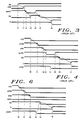
- a timing diagram of normal operation for a transition of signal AN is shown in FIG. 3. At a time t0, signal AN makes a transition. The particular transition shown is from a logic low to a logic high.
- Input circuit 19 and buffer 21 respond to switch signal ANB from a logic low to a logic high at a time t1 about 5 nanoseconds after time t0.
- Transition detector 15 responds to buffer 21 by causing signal *ANTX to become active (a logic low) at a time t2 about 2 nanoseconds after time t1. Signal *ANTX remains low for about 8 nanoseconds.
- EQ generator 18 responds by activating pulse EQ at a time t3 about 4 nanoseconds after time t2. when pulse *ANTX switches back to a logic high at time t4, EQ generator 18 responds by causing pulse EQ to switch to a logic low at a time t5 about 4 nanoseconds following time t4. Valid data D appears at a time t6 about 10 nanoseconds following time t5. This is the desired operation.
- the access time, the time from to to t6, is 29 nanoseconds. This is given as an example.
- the actual times are highly dependent upon the actual process used in the manufacturing of the memory. The times given are comparable to those for a high speed state of the art process.
- FIG. 4 Shown in FIG. 4 is a timing diagram for the operation of circuit 11 of FIG. 2 when memory 10 comes of the deselect mode.
- chip select signal *CS switches from a logic high to a logic low so that memory 10 is then selected.
- Address signal is assumed to be a continuous logic low.
- transistor 24 With signal AN at a logic low, transistor 24 is non-conductive.
- chip select signal *CS is a logic high so that buffer 16 provides signal *CSB also at a logic high.
- signal *CSB With signal *CSB at a logic high transistor 25 is conductive and transistor 22 is non-conductive, disabling input circuit 19 and causing signal *ANI to be a logic low. This is the conventional technique which is effective in reducing power loss during the deselect mode.
- buffer 16 provides signal *CSB to input circuit 19 at a logic low, enabling input circuit 19 by causing transistor 22 to be conductive and transistor 25 to be non-conductive.
- input circuit 19 responds to signal *CSB switching to a logic low at a time t1 by causing signal *ANI to switch to a logic high.
- Buffer 21 responds to signal *ANI switching logic state by causing signal ANB to switch logic state at time t2.
- Transition detector 15 responds to signal ANB switching state by activating pulse *ANTX at a time t3.
- Buffer 21, generates signals in addition to signal ANB.
- Signal ANB is conveniently used for noting the delay incurred in buffering signal AN.
- the delay caused by buffer 16 is about 5 nanoseconds.
- the delay between signal AN and ANB via input circuit 19 and buffer 21 is also about 5 nanoseconds. Consequently, the time between time t0 and time t2 is about 10 nanoseconds.
- the time delay between signal ANB switching logic state and pulse *ANTX being activated is about 2 nanoseconds so that the time between t2 and t3 is 2 nanoseconds.
- signal EQ is a logic high when pulse *ANTX becomes active.
- Signal *CSD is maintained at a logic low for a predetermined time delay following signal *ANB switching to a logic low.
- Signal *CSD at a logic high causes pulse EQ to be a logic high. Consequently, during the deselect mode pulse EQ is held at a logic high so that the memory array is equillibrated during the deselect mode. For a transition from the deselect to select modes, pulse EQ is held at a logic high long enough to let the circuitry stabilize.
- the predetermined delay between signal *CSB and signal *CSD is determined by delay circuit 17.
- the delay is set sufficiently long to avoid pulse EQ switching to a logic low before signal *ANTX, or some other address transition pulse, would cause it to switch to a logic high. Consequently, the switching of pulse *ANTX to a logic low at time t3 does not cause the activation of pulse EQ because pulse EQ is being held at a logic high by signal *CSD.
- Signal *CSD switches to a logic low at time t4, releasing EQ generator 18 to the control of the address transition pulses, pulses AOTX-ANTX.
- pulse *ANTX has switched to a logic low at time t3, causing pulse EQ to remain at a logic high.
- Pulse EQ cannot switch to a logic low until, signal *ANTX switches to a logic high at a time t5, about 8 nanoseconds after time t3. Consequently, the elapsed time from to to t5 is 20 nanoseconds. Pulse EQ switches to a logic low at a time t6 about 4 nanoseconds after pulse *ANTX switches to a logic high. Valid data follows at a time t7 about 10 nanoseconds after pulse EQ switches to a logic low. Consequently, the access time, the time from t0 to t7 is about 34 nanoseconds for switching from the deselect to select modes. Consequently, the access time for a chip select transition is about 5 nanoseconds longer than the access time for an address transition.
- the time from the transition of signal ANB to valid data is the same, about 24 nanoseconds, for both cases. The difference is in the time from to to the transition of signal ANB.
- buffer 16 causes a 5 nanosecond delay before enabling input circuit 19.
- the enabling of input circuit 19 causes a transition of signal *ANI which in turn causes pulse *ANTX to be activated in the case in which address signal AN is a logic low. Consequently, even though no address transition has occurred, signal *ANTX is activated. This is known as a false address transition. This occurs for address input circuits which are disabled by a chip select signal during the deselect mode. This false address transition only occurs when the address signal is a logic low.
- signal *ANI When signal AN is a logic high, signal *ANI will be a logic low even when input circuit is disabled because transistor 24 is conductive. Consequently, the enabling of input circuit 19 does not cause a transition of signal *ANI. Of course it is not knowable in which state the addresses will be. The memory must be prepared to handle this false address transition.
- the access time is extended by about 5 nanoseconds and is specified as such.
- the access time for a transition from the deselect to select modes is specified as 5 nanoseconds longer than for an access time caused by an address transition during the select mode.
- the other manifestation has been simply to not disable the input circuits during the deselect mode. This results in higher current during the deselect mode.
- the deselect mode is also known as standby. Not disabling the input circuits results in specifying a higher standby current.
- Circuit 30 is for replacing circuit 11 in memory 10.
- Circuit 30 is comprised generally of input pads 12, 31, 32, 33 and 34, the chip select buffer 16, a plurality of address input buffers 36, a plurality of transition detectors 37, a chip select delay circuit 38, and an EQ generator 39.
- Plurality of input buffers 36 comprises address input amplifiers 41, 42, 43 and 44.
- Plurality of transition detectors 37 comprises transition detectors 46, 47, 48 and 49.
- Chip select delay circuit 38 comprises a delay circuit 51, a NOR gate 52, an inverter 53, an OR gate 54, a NAND gate 55, and an inverter 56.
- NOR gate 52 has a first input for receiving signal *CSB which is generated in the same way as shown in FIG. 2, a second input, and an output.
- Delay circuit 51 has an input for receiving signal *CSB and an output connected to the second input of NOR gate 52.
- Inverter 53 has an input connected to the output of NOR gate 52 and an output for providing a first delayed chip select signal *CSD1.
- OR gate 54 has a first input connected to the output of delay circuit 51, a second input for receiving signal *CSB, and an output.
- NAND gate 55 has a first input connected to the output of OR gate 54, a second input connected to the output of inverter 53, and an output.
- Inverter 56 has an input connected to the output of NAND gate 55, and an output for providing a second delayed chip select signal *CSD2.
- Input pads 31, 32, 33 and 34 receive address signals A0, A1, A2 and AN, respectively.
- Address input amplifiers 41, 42, 43 and 44 each have an input for receiving a corresponding address signal and an output for providing a buffered address signal.
- Amplifiers 41, 42, 43 and 44 receive address signals A0, A1, A2 and AN, respectively, and provide corresponding buffered address signals A0B, A1B, A2B and ANB, respectively, as well as other signals via buses 61, 62, 63 and 64, respectively.
- Address input amplifiers 41-44 each operate the same as address input amplifier 14 of FIG.
- transition detectors 46, 47, 48 and 49 receive signals relating to corresponding address signals A0, A1, A2 and AN, respectively, via buses 61, 62, 63 and 64, respectively.
- Transition detectors 46, 47, 48 and 49 are connected to amplifiers 41, 42, 43 and 44, respectively, via buses 61, 62, 63 and 64, respectively.
- Transition detectors 46-49 each have a control input for receiving signal *CSD2 by being connected to the output of inverter 56.
- Transition detectors 46, 47, 48 and 49 each have an output for providing an address transition pulse.
- Transition detectors 46, 47, 48 and 49 provide pulses *A0TX, *A1TX, *A2TX and *ANTX.
- Transition detectors 46-49 operate substantially the same as transition detector 15 of FIG. 2 except that when signal *CSD2 is a logic high, transition detectors 46-49 are disabled.
- EQ generator 39 is connected to the outputs of transition detectors 46-49 and the output of inverter 53 and provides signal EQ.
- EQ generator 39 is functionally the same as EQ generator 18 of FIG. 2.
- circuit 30 operates the same as circuit 11 of FIG. 2.
- An address transition causes pulse EQ and subsequent valid data with the same chain reaction as shown in the timing diagram of FIG. 3.
- signals *CSB With signal *CSB at a logic low, signals *CSD1 and *CSD2 will also be a logic low.
- transition detectors 46-49 With signal *CSD2 at a logic low, transition detectors 46-49 are enabled so that they will respond to an address transition by activating the corresponding address transition pulse A0TX-ANTX.
- EQ generator 39 will respond to an activated address transition pulse A0TX-ANTX by activating pulse EQ.
- the improvement over circuit 11 of FIG. 2 is for the case in which a data access is initiated by a transition from the deselect to select modes.
- signal *CSB is a logic high which disables amplifiers 41-44 and causes signals *CSD1 and *CSD2 to be a logic high.
- signal *CSD2 a logic high, transition detectors 46-49 are disabled.
- Pulse EQ is active due to signal *CSD1 being a logic high.
- signal *CSB switches to a logic low to cause the switch from the deselect mode to the select mode, amplifiers 41-44 are enabled, causing signals A0B-ANB to assume the logic state of corresponding address signals A0-AN.
- the corresponding buffered address signals will undergo a logic high to logic low transition.
- FIG. 6 Shown in FIG. 6 is a timing diagram for the case in which signal AN is a logic low when signal *CS switches from a logic high to a logic low at a time t0.
- Signal *CS switching to a logic low causes signal *CSB to switch to a logic low at a time t1 which in turn causes the false transition of signal ANB which switches to a logic low at a time t2.
- An elapsed time for t0 to t2 in FIG. 6 is the same as that shown in FIG. 4, about 10 nanoseconds.
- Signal *ANTX is not generated because signal *CSD2 is kept at a logic high sufficiently long to ensure that the false transitions have ceased.
- Signal *CSD2 will remain at a logic high until both inputs of OR gate 54 are a logic low or until signal *CSD1 switches to a logic low. Both signal *CSD1 and *CSD2 are held to a logic high by delay circuit 51 for a predetermined time delay following signal *CSB switching to a logic low. When signal *CSB switches to a logic low, delay circuit 51 does not output a logic low until the predetermined delay time has elapsed. With NOR gate 52 receiving a logic high for the predetermined delay time, signal *CSD1 will be held at a logic high as well. With the output of delay circuit 51 and signal *CSD1 both at a logic high, signal *CSD2 is also held at a logic high.
- the output of delay circuit 51 switches to a logic low, causing signals *CSD1 and *CSD2 to switch to a logic low at virtually the same time.
- the time from the chip select transition to signals *CSD1 and *CSD2 switching to a logic low should be the same as the time from the address transition to the termination of the address transition pulse. In terms of the timing diagrams this means that the time from to to t4 in FIG. 3 should equal the time from t0 to t3 in FIG. 6. This is achieved by so selecting *CSD1.
- the delay time for *CSD1 can be reduced so that a chip select transiton access can occur faster than an address transition access.
- One delayed chip select signal could be used to both suppress the transition detectors and to generate the equalization pulse for the desired time delay following the chip select transition.
- This function was achieved in circuit 30 with signals *CSD1 and *CSD2 to provide a margin of safety.
- Signal *CSD2 which suppresses transition detectors 46-49, will not be generated unless both signal *CSB and signal *CSD1 are a logic high. This guards against the situation in which signal *CSB is a logic high for only a very short time but causes transition detectors to miss an address transition but does not cause the EQ pulse to be active sufficiently long.
- Circuit 30 causes pulse EQ to be generated by signal *CSD1 switching to a logic high which occurs before signal *CSD2 can suppress transition detectors 46-49.
- Transition detector 49 comprises transistors 66, 67, 68, 69, 70, 71, 72, 73, inverter 74, and NOR gate 75.
- Input amplifier 44 comprises an input circuit 77, a buffer circuit 78, and inverters 79, 80, 81, 82, 83 and 84.
- Bus 64 is simply the connections between amplifier 44 and transition detector 49.
- Transition detector 49 uses true and complementary fast address signal ANF and *ANF and true and complementary slow address signals ANS and *ANS in conventional fashion to generate pulse *ANTX in response to a transition of signal AN, except that NOR gate 75 would normally be an inverter and would not receive signal *CSD2.
Landscapes
- Engineering & Computer Science (AREA)
- Microelectronics & Electronic Packaging (AREA)
- Computer Hardware Design (AREA)
- Static Random-Access Memory (AREA)
- Dram (AREA)
Claims (10)
- Speicherschaltkreis (30), der bei Auftreten eines Chipauswahlsignals (CS) freigegeben wird, mit:
einer Mehrzahl von Adreßeingangsgliedern (36), die jeweils ausgebildet sind, ein Adreßsignal zu empfangen und bei Auftreten des Chipauswahlsignals freigegeben zu werden;
einer mit dem Ausgang der Mehrzahl von Adreßeingangsgliedern verbundenen Übergangserfassungseinrichtung (37) zum Erfassen eines Übergangs eines Adreßsignals;
gekennzeichnet durch:
eine Sperreinrichtung (38, 51, 52, 53, 54, 55, 56) zum Sperren der Übergangserfassungseinrichtung (37) für eine vorgegebene Zeitspanne im Anschluß an ein Auftreten des Chipauswahlsignals. - Speicherschaltkreis nach Anspruch 1, der freigegeben wird, sobald das Chipauswahlsignal (CS) von einem ersten logischen Zustand in einen Zweiten logischen Zustand wechselt, wobei
die Mehrzahl von Adreßeingangsgliedern durch den zweiten logischen Zustand des Chipauswahlsignals freigegeben und durch den ersten logischen Zustand des Chipauswahlsignals gesperrt werden und jedes Adreßeingangsglied (41, 42, 43, 44) bei Freigabe durch das Chipauswahlsignal ein das empfangene Adreßsignal repräsentierendes Ausgangssignal liefert und bei Sperrung durch das Chipauswahlsignal das Ausgangssignal in einem vorbestimmten Zustand ausgibt;
die Übergangserfassungseinrichtung eine Mehrzahl von Übergangserfassungseinrichtungen (46, 47, 48, 49) umfaßt, von denen jede mit einem zugeordneten Adreßeingangsglied (41, 42, 43, 44) verbunden ist und ausgebildet ist, einen Übergang des Ausgangssignals des zugeordneten Adreßeingangsglieds zu erfassen; und
die Sperreinrichtung (38) die Mehrzahl von Übergangserfassungseinrichtungen für die vorgegebene Verzögerungszeit alle sperrt, sobald das Chipauswahlsignal vom ersten in den zweiten logischen Zustand wechselt. - Speicherschaltkreis nach Anspruch 2, bei dem jede freigegebene Übergangserfassungseinrichtung (46, 47, 48, 49) einen Ausgangsimpuls liefert, wenn sie einen Adreßübergang des Ausgangssignals des zugeordneten Adreßeingangsglieds (41, 42, 43, 44) erfaßt.
- Speicherschaltkreis nach Anspruch 3, ferner mit einem mit der Mehrzahl von Übergangserfassungseinrichtungen (37) verbundenen Abgleichimpulsgenerator (39) zum Erzeugen eines Abgleichimpulses (EQ) bei Empfang eines Ausgangsimpulses.
- Speicherschaltkreis nach Anspruch 4, bei dem die Sperreinrichtung ein verzögertes Chipauswahlsignal (CSD) liefert, wenn das Chipauswahlsignal den Speicherschaltkreis sperrt.
- Speicherschaltkreis nach Anspruch 5, bei dem der Abgleichimpulsgenerator den Abgleichimpuls liefert, wenn das verzögerte Chipauswahlsignal vorliegt.
- Verfahren zum Freigeben eines Speicherschaltkreises bei Auftreten eines Chipauswahlsignals (CS), wobei der Speicherschaltkreis folgende Merkmale aufweist:
ein Eingangsglied (36) zum Empfangen eines Adreßsignals;
eine mit dem Ausgang des Eingangsglieds verbundene Übergangserfassungseinrichtung (37); und
einen mit der Übergangserfassungseinrichtung verbundenen Abgleichimpulsgenerator (39);
und wobei das Verfahren folgende Schritte umfaßt:
Ausgeben eines Ausgangssignals am Ausgang des Eingangsglieds bei Empfang des Adreßsignals, wenn das Eingangsglied durch ein Auftreten des Chipauswahlsignals freigegeben ist, und Ausgeben des Ausgangssignals in einem vorbestimmten Zustand, wenn das Eingangsglied durch das Chipauswahlsignal gesperrt ist;
Erfassen eines Übergangs des Adreßsignals;
Erzeugen eines Abgleichimpulses (EQ) bei Erfassung eines Übergangs des Adreßsignals;
gekennzeichnet durch die Verfahrensschritte, daß die Übergangserfassungseinrichtung im Anschluß an ein Auftreten des Chipauswahlsignals zumindest für eine vorgegebene Zeitspanne daran gehindert wird, einen Übergang des Adreßsignals zu erfassen. - Verfahren nach Anspruch 7, mit den weiteren Schritten, daß der Abgleichimpuls im Anschluß an das Auftreten des Chipauswahlsignals zumindest für die vorgegebene Zeitspanne bereitgestellt wird.
- Verfahren nach Anspruch 8, mit den weiteren Schritten, daß
der Abgleichimpuls bei Beendigung eines ersten Verzögerungssignals (CSD1) beendet wird; und
das Verhindern der Erfassung eines Adreßsignalübergangs bei Beendigung eines zweiten Verzögerungssignals (CSD2) beendet wird. - Verfahren nach Anspruch 9, wobei das erste Verzögerungssignal vor Beendigung des zweiten Verzögerungssignal beendet wird.
Applications Claiming Priority (2)
| Application Number | Priority Date | Filing Date | Title |
|---|---|---|---|
| US750638 | 1985-07-01 | ||
| US06/750,638 US4630239A (en) | 1985-07-01 | 1985-07-01 | Chip select speed-up circuit for a memory |
Publications (3)
| Publication Number | Publication Date |
|---|---|
| EP0222833A1 EP0222833A1 (de) | 1987-05-27 |
| EP0222833A4 EP0222833A4 (en) | 1990-10-24 |
| EP0222833B1 true EP0222833B1 (de) | 1992-12-16 |
Family
ID=25018658
Family Applications (1)
| Application Number | Title | Priority Date | Filing Date |
|---|---|---|---|
| EP86903098A Expired - Lifetime EP0222833B1 (de) | 1985-07-01 | 1986-05-05 | Chipauswahlbeschleunigungsschaltung für einen speicher |
Country Status (8)
| Country | Link |
|---|---|
| US (1) | US4630239A (de) |
| EP (1) | EP0222833B1 (de) |
| JP (1) | JPH0762957B2 (de) |
| KR (1) | KR920009667B1 (de) |
| DE (1) | DE3687302T2 (de) |
| HK (1) | HK85795A (de) |
| SG (1) | SG32572G (de) |
| WO (1) | WO1987000340A1 (de) |
Families Citing this family (17)
| Publication number | Priority date | Publication date | Assignee | Title |
|---|---|---|---|---|
| US4884198A (en) * | 1986-12-18 | 1989-11-28 | Sun Microsystems, Inc. | Single cycle processor/cache interface |
| US5018109A (en) * | 1987-01-16 | 1991-05-21 | Hitachi, Ltd. | Memory including address registers for increasing access speed to the memory |
| US5175826A (en) * | 1988-05-26 | 1992-12-29 | Ibm Corporation | Delayed cache write enable circuit for a dual bus microcomputer system with an 80386 and 82385 |
| NL9001500A (nl) * | 1990-07-02 | 1992-02-03 | Philips Nv | Geintegreerde schakeling voorzien van een invoer buffer schakeling. |
| JPH0474384A (ja) * | 1990-07-17 | 1992-03-09 | Toshiba Corp | 半導体集積回路装置 |
| JPH04258885A (ja) * | 1991-02-12 | 1992-09-14 | Mitsubishi Electric Corp | 半導体記憶装置 |
| JP3007475B2 (ja) * | 1992-06-05 | 2000-02-07 | 三菱電機株式会社 | メモリ装置 |
| US5306963A (en) * | 1992-06-19 | 1994-04-26 | Intel Corporation | Address transition detection noise filter in pulse summation circuit for nonvolatile semiconductor memory |
| US5301165A (en) * | 1992-10-28 | 1994-04-05 | International Business Machines Corporation | Chip select speedup circuit for a memory |
| US5418479A (en) * | 1993-12-27 | 1995-05-23 | Intel Corporation | Method and circuitry for generating a safe address transition pulse in a memory device |
| JP2953297B2 (ja) * | 1994-03-30 | 1999-09-27 | 日本電気株式会社 | 受光素子およびその駆動方法 |
| FR2720852B1 (fr) * | 1994-06-01 | 1996-08-02 | Matra Mhs | Dispositif de détection de transition engendrant une impulsion de durée variable. |
| KR100214564B1 (ko) * | 1997-04-12 | 1999-08-02 | 구본준 | 균등화 신호 발생기 |
| KR100295682B1 (ko) * | 1999-04-07 | 2001-07-12 | 김영환 | 데이터 입력 버퍼 회로 |
| US20030018846A1 (en) * | 2001-07-18 | 2003-01-23 | Blaise Fanning | Method and system for fast memory initialization or diagnostics |
| TWI436371B (zh) * | 2010-11-02 | 2014-05-01 | Etron Technology Inc | 具低功耗之或線比對電路 |
| US11508422B2 (en) | 2019-08-02 | 2022-11-22 | Micron Technology, Inc. | Methods for memory power management and memory devices and systems employing the same |
Family Cites Families (4)
| Publication number | Priority date | Publication date | Assignee | Title |
|---|---|---|---|---|
| US4344156A (en) * | 1980-10-10 | 1982-08-10 | Inmos Corporation | High speed data transfer for a semiconductor memory |
| US4575823A (en) * | 1982-08-17 | 1986-03-11 | Westinghouse Electric Corp. | Electrically alterable non-volatile memory |
| JPS59151385A (ja) * | 1983-01-28 | 1984-08-29 | Toshiba Corp | メモリ素子の信号変化検出回路 |
| US4614883A (en) * | 1983-12-01 | 1986-09-30 | Motorola, Inc. | Address transition pulse circuit |
-
1985
- 1985-07-01 US US06/750,638 patent/US4630239A/en not_active Expired - Lifetime
-
1986
- 1986-05-05 JP JP61502660A patent/JPH0762957B2/ja not_active Expired - Lifetime
- 1986-05-05 SG SG1995906152A patent/SG32572G/en unknown
- 1986-05-05 KR KR1019870700177A patent/KR920009667B1/ko not_active Expired
- 1986-05-05 DE DE8686903098T patent/DE3687302T2/de not_active Expired - Fee Related
- 1986-05-05 EP EP86903098A patent/EP0222833B1/de not_active Expired - Lifetime
- 1986-05-05 WO PCT/US1986/000979 patent/WO1987000340A1/en not_active Ceased
-
1995
- 1995-06-01 HK HK85795A patent/HK85795A/en not_active IP Right Cessation
Also Published As
| Publication number | Publication date |
|---|---|
| JPH0762957B2 (ja) | 1995-07-05 |
| KR880700431A (ko) | 1988-03-15 |
| KR920009667B1 (ko) | 1992-10-22 |
| DE3687302T2 (de) | 1993-04-15 |
| WO1987000340A1 (en) | 1987-01-15 |
| HK85795A (en) | 1995-06-09 |
| US4630239A (en) | 1986-12-16 |
| JPS62503196A (ja) | 1987-12-17 |
| EP0222833A1 (de) | 1987-05-27 |
| SG32572G (en) | 1995-09-01 |
| EP0222833A4 (en) | 1990-10-24 |
| DE3687302D1 (de) | 1993-01-28 |
Similar Documents
| Publication | Publication Date | Title |
|---|---|---|
| EP0222833B1 (de) | Chipauswahlbeschleunigungsschaltung für einen speicher | |
| US4718043A (en) | Memory circuit with improved power-down control | |
| US5563835A (en) | Sense amplification in data memories | |
| JPS621191A (ja) | 信号出力回路 | |
| US4614883A (en) | Address transition pulse circuit | |
| US5841706A (en) | Semiconductor memory device capable of high speed operation in low power supply voltage | |
| JPS62212996A (ja) | メモリのビツト・ライン等化装置 | |
| US4689771A (en) | Memory with improved write mode to read mode transition | |
| US4918658A (en) | Static random access memory with asynchronous power-down | |
| US5301165A (en) | Chip select speedup circuit for a memory | |
| US4742493A (en) | Multiple port memory array device including improved timing and associated method | |
| US5268873A (en) | Semiconductor memory apparatus | |
| US5936909A (en) | Static random access memory | |
| EP0105757B1 (de) | Asynchrone Halbleiterspeicheranordnung | |
| US5228003A (en) | Semiconductor memory | |
| US6169702B1 (en) | Memory device having a chip select speedup feature and associated methods | |
| US6181613B1 (en) | Semiconductor memory device operable in burst mode and normal mode through improved switching operations | |
| US6122221A (en) | Scheme for increasing enable access speed in a memory device | |
| JP3168581B2 (ja) | 半導体記憶装置 | |
| US4958319A (en) | Address amplifier circuit having automatic interlock and protection against multiple addressing for use in static GaAs RAMs | |
| KR950010142B1 (ko) | 라이트 인에이블 (we) 버퍼 보호 회로 | |
| KR0167690B1 (ko) | 어드레스 교란을 제거한 반도체 메모리 장치 | |
| US5629902A (en) | Semiconductor memory device | |
| KR20010004658A (ko) | 어드레스 스트로브장치 | |
| US6243303B1 (en) | Method and circuitry for writing data |
Legal Events
| Date | Code | Title | Description |
|---|---|---|---|
| PUAI | Public reference made under article 153(3) epc to a published international application that has entered the european phase |
Free format text: ORIGINAL CODE: 0009012 |
|
| 17P | Request for examination filed |
Effective date: 19870302 |
|
| AK | Designated contracting states |
Kind code of ref document: A1 Designated state(s): DE FR GB |
|
| A4 | Supplementary search report drawn up and despatched |
Effective date: 19900905 |
|
| AK | Designated contracting states |
Kind code of ref document: A4 Designated state(s): DE FR GB |
|
| 17Q | First examination report despatched |
Effective date: 19910603 |
|
| GRAA | (expected) grant |
Free format text: ORIGINAL CODE: 0009210 |
|
| AK | Designated contracting states |
Kind code of ref document: B1 Designated state(s): DE FR GB |
|
| REF | Corresponds to: |
Ref document number: 3687302 Country of ref document: DE Date of ref document: 19930128 |
|
| ET | Fr: translation filed | ||
| PLBE | No opposition filed within time limit |
Free format text: ORIGINAL CODE: 0009261 |
|
| STAA | Information on the status of an ep patent application or granted ep patent |
Free format text: STATUS: NO OPPOSITION FILED WITHIN TIME LIMIT |
|
| 26N | No opposition filed | ||
| PGFP | Annual fee paid to national office [announced via postgrant information from national office to epo] |
Ref country code: DE Payment date: 19980423 Year of fee payment: 13 |
|
| REG | Reference to a national code |
Ref country code: GB Ref legal event code: 746 Effective date: 19990325 |
|
| PG25 | Lapsed in a contracting state [announced via postgrant information from national office to epo] |
Ref country code: DE Free format text: LAPSE BECAUSE OF NON-PAYMENT OF DUE FEES Effective date: 20000301 |
|
| PGFP | Annual fee paid to national office [announced via postgrant information from national office to epo] |
Ref country code: GB Payment date: 20000404 Year of fee payment: 15 |
|
| PGFP | Annual fee paid to national office [announced via postgrant information from national office to epo] |
Ref country code: FR Payment date: 20000504 Year of fee payment: 15 |
|
| PG25 | Lapsed in a contracting state [announced via postgrant information from national office to epo] |
Ref country code: GB Free format text: LAPSE BECAUSE OF NON-PAYMENT OF DUE FEES Effective date: 20010505 |
|
| REG | Reference to a national code |
Ref country code: FR Ref legal event code: D6 |
|
| GBPC | Gb: european patent ceased through non-payment of renewal fee |
Effective date: 20010505 |
|
| PG25 | Lapsed in a contracting state [announced via postgrant information from national office to epo] |
Ref country code: FR Free format text: LAPSE BECAUSE OF NON-PAYMENT OF DUE FEES Effective date: 20020131 |