EP0223637A1 - Verfahren zum Herstellen eines metallischen Mehrschicht-Verbindungsmusters für hochintegrierte Schaltungsbauelemente - Google Patents
Verfahren zum Herstellen eines metallischen Mehrschicht-Verbindungsmusters für hochintegrierte Schaltungsbauelemente Download PDFInfo
- Publication number
- EP0223637A1 EP0223637A1 EP86402139A EP86402139A EP0223637A1 EP 0223637 A1 EP0223637 A1 EP 0223637A1 EP 86402139 A EP86402139 A EP 86402139A EP 86402139 A EP86402139 A EP 86402139A EP 0223637 A1 EP0223637 A1 EP 0223637A1
- Authority
- EP
- European Patent Office
- Prior art keywords
- layer
- conductors
- integrated circuit
- dielectric layer
- dielectric
- Prior art date
- Legal status (The legal status is an assumption and is not a legal conclusion. Google has not performed a legal analysis and makes no representation as to the accuracy of the status listed.)
- Granted
Links
Images
Classifications
-
- H—ELECTRICITY
- H10—SEMICONDUCTOR DEVICES; ELECTRIC SOLID-STATE DEVICES NOT OTHERWISE PROVIDED FOR
- H10W—GENERIC PACKAGES, INTERCONNECTIONS, CONNECTORS OR OTHER CONSTRUCTIONAL DETAILS OF DEVICES COVERED BY CLASS H10
- H10W20/00—Interconnections in chips, wafers or substrates
- H10W20/01—Manufacture or treatment
- H10W20/071—Manufacture or treatment of dielectric parts thereof
- H10W20/092—Manufacture or treatment of dielectric parts thereof by smoothing the dielectric parts
-
- H—ELECTRICITY
- H10—SEMICONDUCTOR DEVICES; ELECTRIC SOLID-STATE DEVICES NOT OTHERWISE PROVIDED FOR
- H10W—GENERIC PACKAGES, INTERCONNECTIONS, CONNECTORS OR OTHER CONSTRUCTIONAL DETAILS OF DEVICES COVERED BY CLASS H10
- H10W20/00—Interconnections in chips, wafers or substrates
- H10W20/40—Interconnections external to wafers or substrates, e.g. back-end-of-line [BEOL] metallisations or vias connecting to gate electrodes
- H10W20/41—Interconnections external to wafers or substrates, e.g. back-end-of-line [BEOL] metallisations or vias connecting to gate electrodes characterised by their conductive parts
- H10W20/42—Vias, e.g. via plugs
-
- H—ELECTRICITY
- H10—SEMICONDUCTOR DEVICES; ELECTRIC SOLID-STATE DEVICES NOT OTHERWISE PROVIDED FOR
- H10W—GENERIC PACKAGES, INTERCONNECTIONS, CONNECTORS OR OTHER CONSTRUCTIONAL DETAILS OF DEVICES COVERED BY CLASS H10
- H10W20/00—Interconnections in chips, wafers or substrates
- H10W20/40—Interconnections external to wafers or substrates, e.g. back-end-of-line [BEOL] metallisations or vias connecting to gate electrodes
- H10W20/45—Interconnections external to wafers or substrates, e.g. back-end-of-line [BEOL] metallisations or vias connecting to gate electrodes characterised by their insulating parts
- H10W20/48—Insulating materials thereof
Definitions
- the invention relates to a method for forming a multilayer metallic network for interconnecting the components of a high density integrated circuit, as well as to the resulting integrated circuit, commonly called a chip or VLSI chip (Very Large Scale Integration). ).
- Conventional methods of forming a multilayer network for interconnecting the components of a chip essentially consist in forming a metal layer on a dielectric layer covering a lower metal layer composed of conductors.
- the conductive layers are usually made of aluminum and have a thickness of the order of a micrometer.
- the lower metal layer has a uniform thickness and covers a base surface extending over the components of the chip.
- the conductors are usually etched by placing the lower metal layer under reactive plasma. This engraving is practically anisotropic. It is carried out in the thickness direction of the layer and thus gives the conductors an approximately rectangular section.
- the typical pitch of metallic conductors is 6 micrometers (6 ⁇ m) for a width of 3 ⁇ m, and it is desirable that these dimensions can be lowered.
- the etched layer is then covered with a dielectric layer ordinarily made by a chemical deposition of mineral silicon dioxide (SiO2) in the vapor phase.
- a dielectric layer ordinarily made by a chemical deposition of mineral silicon dioxide (SiO2) in the vapor phase.
- the typical thickness of this layer is of the order of 0.8 ⁇ m. It is desirable that the dielectric layer have a uniform thickness over the entire metal layer lower to ensure satisfactory and uniform electrical insulation between the two metal layers.
- This technique currently poses serious problems, detrimental to the desired density of the interconnection network and caused essentially by the abrupt edges of the conductors of the lower layer.
- experience shows a withdrawal of the dielectric in the angles made by the conductors with their base surface in a plane perpendicular to the conductors. More specifically, the thickness of the dielectric layer gradually decreases towards the top of each bottom angle, tangentially to a straight line approximately corresponding to the bisector of the angle, hereinafter called bisector for convenience.
- this layer already has the drawback of offering defective insulation between the metal layers in the corners of the bottom.
- the deposition of the upper conductive layer on the dielectric layer poses in practice the major problem, since it will obviously considerably amplify the defects in covering of the dielectric layer. Indeed, the experiment reveals a very pronounced thinning of the conductive layer, tangential to the bisector of the angles of the bottom.
- the metallic layer seen in each bottom angle and in a plane normal to the conductors thus takes the form of two adjacent lips, tangential to the bisector plane of the bottom angle.
- the thinning present at the junction of the lips creates an undesirable electrical resistance, which the layer accumulates in all of its bottom angles.
- the solution currently adopted to overcome this serious drawback has been to produce conductive micrograins between the lips of the upper conductive layer in each corner of the bottom.
- the etching is also preferably done under reactive plasma, the duration of which is determined by the thickness of the layer to be etched. Since the etching under reactive plasma is anisotropic and that it is normally done on the general plane of the chip, the duration of the etching is determined by the thickness of the conductive layer in this direction.
- the thickness of the conductive layer in this direction can reach a value twice that of the other parts of the layer which determine the time of the etching. Etching must therefore be continued until complete elimination of the conductive parts on the stiff edges of the dielectric layer in order to ensure perfect electrical insulation between neighboring conductors.
- the additional duration of the engraving significantly alters its quality.
- the shape of the lip which the dielectric layer has on the steep edges of the lower conductive layer poses a particularly important and practically insoluble problem for the etching of the upper conductive layer.
- the top of the lip of the dielectric layer screens the metal part placed in the shadow area of the reactive plasma. The etching therefore turns out to be imperfect, leaving residual conductive parts with unfortunate consequences, often intolerable (risk of short circuit, etc.).
- the invention solves all of these problems by making the support surface of the upper metal layer approximately planar.
- the method according to the invention for forming a multilayer metallic network for interconnecting the components of a high density integrated circuit consisting of forming a lower metallic layer including conductors with stiff sides, chemically depositing a vapor dielectric layer on the lower metal layer, to provide openings in the dielectric layer above the conductors, and to cover the dielectric layer of an upper metal layer, is characterized in that it consists in filling approximately the gaps formed by the dielectric layer in the intervals between the conductors, by spreading a viscous dielectric suspension and by annealing the suspension, and in addition passing through the layer obtained by annealing in order to provide the openings.
- the invention also relates to the high density integrated circuit which results from the implementation of this method.
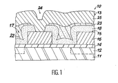
- the high density integrated circuit (10) shown in Figure 1 consists of a semiconductor substrate (11) incorporating a set of components (12) illustrated schematically, and a metal network (13) for the interconnection of components (12 ) of the substrate (11).
- the network (13) generally has as its base surface the upper surface of an insulation layer (14) covering the substrate (11).
- MOS technology Metal-Oxide-Semiconductor
- the metal network (13) often covers a primary layer of interconnection conductors in polycrystalline silicon. Since the polycrystalline conductors do not pose the problems solved by the invention, these conductors are not shown in FIG. 1, but it is clear that an integrated circuit according to the invention can incorporate them.
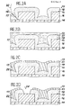
- the description of the interconnection network (13) of the integrated circuit (10) shown in Figure 1 will now be made by following its manufacturing process illustrated in Figures 2A-2D.
- the interconnection network (13) firstly comprises, in a conventional manner, a lower conducting layer (15) covering the upper face of the insulation layer (14).
- the layer (15) is composed of metallic conductors (16) separated by intervals (17).
- the conductors (16) are generally parallel to each other, in the direction perpendicular to the planes of the figures illustrated, and have a substantially rectangular section. This section is due to etching under reactive plasma of an initial metal layer uniformly covering the insulation layer (14). Certain variants of this engraving make it possible to obtain less stiff fronts, which nevertheless pose the same problems as those with vertical sides.
- the expression “conductors with steep sides” must therefore be understood to include conductors whose inclination of the sides poses the same problems as those set out previously and illustrated below.
- a dielectric layer (18) is deposited on the whole of the lower layer (15). It is usually made of mineral silicon dioxide chemically deposited in the vapor phase.
- the experience reveals that a shrinkage of the thickness of the dielectric layer (18) occurs in the corners of the bottom of the layer (15), that is to say the angles which the conductors (16) form with the layer d insulation (14).
- this withdrawal gives the layer a profile of lips which, in the plane of the figures, converge tangentially to a straight line (19) corresponding approximately to the bisector of each angle. This phenomenon is due to the steep sides of the conductors and is independent of the way of depositing the layer (18).
- the invention consists in filling at least partially the recesses existing in the gaps (17) between the conductors (16), so as to give the upper metallic layer a roughly planar base surface.
- a viscous dielectric suspension (21) is deposited on the integrated circuit (10), then spread uniformly over the entire surface of the dielectric layer (18).
- the suspension (21) has been put in sufficient quantity to overflow the hollows formed by the dielectric layer (18) in the intervals (17).
- the spreading will preferably be obtained by the rotation of the semiconductor wafer (wafer) including the integrated circuit (10), at a speed determined so that the centrifugal force comes into equilibrium with the viscosity forces of the suspension.
- the suspension may be a gel based on mineral silica, advantageously in colloidal form, such as that commonly called SOG (Spin-On-Glass) well known in the art.
- SOG Spin-On-Glass
- the viscous dielectric suspension is used in the same way as the photosensitive resins used for the configuration of the elements of the integrated circuit.
- the solvent in the suspension evaporates while the dielectric forms a compact mass (22) as shown in FIG. 2C.
- the mass (22) is essentially located in the gaps (17), but also covers with a thin film (23) the dielectric layer (18) located above the conductors (16).
- the films (23) will always exist, whatever the degree of filling of the recesses in the intervals (17), because of the viscosity of the suspension (21) and of its spreading.
- the contact openings (24) are formed above the conductors (16) for their connection with the upper metallic layer which will be deposited later.
- the openings (24) are also usually etched under reactive plasma. Normal etching would therefore create stiff sides similar to those of the conductors (16) and produce the same phenomenon of shrinkage of the upper layer in the corners of the bottom of the openings (24).
- a classic variant of the engraving is used, which flares the openings and also makes the corners of the bottom very obtuse. The flare angle depends in particular on the nature of the engraved material.
- each opening (24) results in a profile composed of two coaxial frustoconical parts, relative to the film (23 ) and the layer (18), the part relating to the film (23) being more flared.
- this variant of reactive plasma etching is not adopted for the training of conductors (16), since it would significantly reduce their section and would oppose the development of very high densities sought from the interconnection network (13).
- the deposition of the upper metal layer (25) results in the configuration shown in FIG. 1.
- the layer (25) can later serve as a lower layer for implementing the process according to the invention for forming an interconnection network (13) with three metallic layers.
Landscapes
- Internal Circuitry In Semiconductor Integrated Circuit Devices (AREA)
- Local Oxidation Of Silicon (AREA)
Applications Claiming Priority (2)
| Application Number | Priority Date | Filing Date | Title |
|---|---|---|---|
| FR8514669A FR2588417B1 (fr) | 1985-10-03 | 1985-10-03 | Procede de formation d'un reseau metallique multicouche d'interconnexion des composants d'un circuit integre de haute densite et circuit integre en resultant |
| FR8514669 | 1985-10-03 |
Publications (2)
| Publication Number | Publication Date |
|---|---|
| EP0223637A1 true EP0223637A1 (de) | 1987-05-27 |
| EP0223637B1 EP0223637B1 (de) | 1991-08-28 |
Family
ID=9323497
Family Applications (1)
| Application Number | Title | Priority Date | Filing Date |
|---|---|---|---|
| EP86402139A Expired - Lifetime EP0223637B1 (de) | 1985-10-03 | 1986-10-01 | Verfahren zum Herstellen eines metallischen Mehrschicht-Verbindungsmusters für hochintegrierte Schaltungsbauelemente |
Country Status (5)
| Country | Link |
|---|---|
| US (1) | US4906592A (de) |
| EP (1) | EP0223637B1 (de) |
| JP (1) | JPS62174949A (de) |
| DE (1) | DE3681124D1 (de) |
| FR (1) | FR2588417B1 (de) |
Cited By (6)
| Publication number | Priority date | Publication date | Assignee | Title |
|---|---|---|---|---|
| EP0312154A1 (de) * | 1987-10-16 | 1989-04-19 | Koninklijke Philips Electronics N.V. | Methode zur Ausbildung von Verbindungen zwischen leitenden Ebenen |
| EP0221798B1 (de) * | 1985-10-03 | 1989-12-06 | Bull S.A. | Verfahren zum Herstellen eines metallischen Verbindungsmusters für hochintegrierte Schaltungsbauelemente |
| EP0360992A3 (en) * | 1988-09-29 | 1990-08-29 | Sgs-Thomson Microelectronics S.R.L. | A dielectric layer of first interconnection for electronic semiconductor devices |
| EP0380327A3 (de) * | 1989-01-25 | 1990-12-12 | Nec Corporation | Struktur einer Halbleiteranordnung mit einer trichterförmigen Verbindung zwischen den Ebenen |
| EP0450558A3 (en) * | 1990-04-02 | 1992-04-29 | Kabushiki Kaisha Toshiba | Semiconductor device and method of manufacturing the same |
| EP0420405A3 (en) * | 1989-08-31 | 1992-06-24 | Delco Electronics Corporation | Integrated circuit comprising interconnections |
Families Citing this family (18)
| Publication number | Priority date | Publication date | Assignee | Title |
|---|---|---|---|---|
| JPH0277140A (ja) * | 1988-09-13 | 1990-03-16 | Nec Corp | 集積回路の製造方法 |
| US5164339A (en) * | 1988-09-30 | 1992-11-17 | Siemens-Bendix Automotive Electronics L.P. | Fabrication of oxynitride frontside microstructures |
| DE69031543T2 (de) * | 1989-02-17 | 1998-04-09 | Matsushita Electronics Corp | Verfahren zum Herstellen einer Halbleitervorrichtung |
| US5037777A (en) * | 1990-07-02 | 1991-08-06 | Motorola Inc. | Method for forming a multi-layer semiconductor device using selective planarization |
| US5413966A (en) * | 1990-12-20 | 1995-05-09 | Lsi Logic Corporation | Shallow trench etch |
| US5290396A (en) * | 1991-06-06 | 1994-03-01 | Lsi Logic Corporation | Trench planarization techniques |
| JP2665404B2 (ja) * | 1991-02-18 | 1997-10-22 | シャープ株式会社 | 半導体装置の製造方法 |
| US5248625A (en) * | 1991-06-06 | 1993-09-28 | Lsi Logic Corporation | Techniques for forming isolation structures |
| US5252503A (en) * | 1991-06-06 | 1993-10-12 | Lsi Logic Corporation | Techniques for forming isolation structures |
| US5225358A (en) * | 1991-06-06 | 1993-07-06 | Lsi Logic Corporation | Method of forming late isolation with polishing |
| JPH06278468A (ja) * | 1993-03-18 | 1994-10-04 | Nissan Motor Co Ltd | トランクリッド構造 |
| JPH0817174B2 (ja) * | 1993-11-10 | 1996-02-21 | キヤノン販売株式会社 | 絶縁膜の改質方法 |
| US5658829A (en) * | 1995-02-21 | 1997-08-19 | Micron Technology, Inc. | Semiconductor processing method of forming an electrically conductive contact plug |
| US5710460A (en) * | 1995-04-21 | 1998-01-20 | International Business Machines Corporation | Structure for reducing microelectronic short circuits using spin-on glass as part of the interlayer dielectric |
| US5597764A (en) * | 1996-07-15 | 1997-01-28 | Vanguard International Semiconductor Corporation | Method of contact formation and planarization for semiconductor processes |
| US6010957A (en) * | 1997-06-25 | 2000-01-04 | Advanced Micro Devices | Semiconductor device having tapered conductive lines and fabrication thereof |
| KR100602131B1 (ko) * | 2004-12-30 | 2006-07-19 | 동부일렉트로닉스 주식회사 | 반도체 소자 및 그의 제조방법 |
| US7517810B2 (en) * | 2005-05-27 | 2009-04-14 | International Rectifier Corporation | Reduced metal design rules for power devices |
Citations (5)
| Publication number | Priority date | Publication date | Assignee | Title |
|---|---|---|---|---|
| US3506880A (en) * | 1963-06-28 | 1970-04-14 | Ibm | Semiconductor device |
| US3542550A (en) * | 1966-09-30 | 1970-11-24 | Ibm | Photosensitive glass technique for forming contact holes in protective glass layers |
| EP0025261A1 (de) * | 1979-07-31 | 1981-03-18 | Fujitsu Limited | Verfahren zur Herstellung einer Halbleitervorrichtung |
| EP0071010A2 (de) * | 1981-07-27 | 1983-02-09 | International Business Machines Corporation | Verfahren zum Ebnen einer integrierten Schaltungsstruktur |
| EP0147203A2 (de) * | 1983-12-27 | 1985-07-03 | Kabushiki Kaisha Toshiba | Verfahren zum Herstellen von Mehrschichtverbindungen für eine Halbleiteranordnung |
Family Cites Families (29)
| Publication number | Priority date | Publication date | Assignee | Title |
|---|---|---|---|---|
| JPS5425178A (en) * | 1977-07-27 | 1979-02-24 | Fujitsu Ltd | Manufacture for semiconductor device |
| JPS54101292A (en) * | 1978-01-27 | 1979-08-09 | Hitachi Ltd | Contact forming method |
| US4349609A (en) * | 1979-06-21 | 1982-09-14 | Fujitsu Limited | Electronic device having multilayer wiring structure |
| US4222792A (en) * | 1979-09-10 | 1980-09-16 | International Business Machines Corporation | Planar deep oxide isolation process utilizing resin glass and E-beam exposure |
| JPS5759359A (en) * | 1980-09-27 | 1982-04-09 | Fujitsu Ltd | Manufacture of semiconductor device |
| US4436582A (en) * | 1980-10-28 | 1984-03-13 | Saxena Arjun N | Multilevel metallization process for integrated circuits |
| JPS57170550A (en) * | 1981-04-15 | 1982-10-20 | Toshiba Corp | Manufacture of semiconductor device |
| JPS5819727A (ja) * | 1981-07-28 | 1983-02-04 | Canon Inc | 回転ヘツド装置 |
| US4576900A (en) * | 1981-10-09 | 1986-03-18 | Amdahl Corporation | Integrated circuit multilevel interconnect system and method |
| JPS5886746A (ja) * | 1981-11-19 | 1983-05-24 | Nec Corp | 半導体装置 |
| JPS5893347A (ja) * | 1981-11-30 | 1983-06-03 | Toshiba Corp | Mos型半導体装置及びその製造方法 |
| CA1169022A (en) * | 1982-04-19 | 1984-06-12 | Kevin Duncan | Integrated circuit planarizing process |
| JPS598440A (ja) * | 1982-07-07 | 1984-01-17 | Hitachi Ltd | 光情報伝送システム |
| JPS5966147A (ja) * | 1982-10-08 | 1984-04-14 | Hitachi Ltd | 多層配線の製造方法 |
| JPS6030153A (ja) * | 1983-07-28 | 1985-02-15 | Toshiba Corp | 半導体装置 |
| US4451326A (en) * | 1983-09-07 | 1984-05-29 | Advanced Micro Devices, Inc. | Method for interconnecting metallic layers |
| KR900004968B1 (ko) * | 1984-02-10 | 1990-07-12 | 후지쓰 가부시끼가이샤 | 반도체장치 제조방법 |
| US4481070A (en) * | 1984-04-04 | 1984-11-06 | Advanced Micro Devices, Inc. | Double planarization process for multilayer metallization of integrated circuit structures |
| US4523372A (en) * | 1984-05-07 | 1985-06-18 | Motorola, Inc. | Process for fabricating semiconductor device |
| US4519872A (en) * | 1984-06-11 | 1985-05-28 | International Business Machines Corporation | Use of depolymerizable polymers in the fabrication of lift-off structure for multilevel metal processes |
| US4545852A (en) * | 1984-06-20 | 1985-10-08 | Hewlett-Packard Company | Planarization of dielectric films on integrated circuits |
| JPS6165454A (ja) * | 1984-09-07 | 1986-04-04 | Fujitsu Ltd | 半導体装置の製造方法 |
| US4541169A (en) * | 1984-10-29 | 1985-09-17 | International Business Machines Corporation | Method for making studs for interconnecting metallization layers at different levels in a semiconductor chip |
| JPS61180458A (ja) * | 1985-02-05 | 1986-08-13 | Nec Corp | 半導体装置の製造方法 |
| US4681795A (en) * | 1985-06-24 | 1987-07-21 | The United States Of America As Represented By The Department Of Energy | Planarization of metal films for multilevel interconnects |
| US4674176A (en) * | 1985-06-24 | 1987-06-23 | The United States Of America As Represented By The United States Department Of Energy | Planarization of metal films for multilevel interconnects by pulsed laser heating |
| JPS6230335A (ja) * | 1985-07-31 | 1987-02-09 | Fujitsu Ltd | 半導体装置の製造方法 |
| US4662064A (en) * | 1985-08-05 | 1987-05-05 | Rca Corporation | Method of forming multi-level metallization |
| US4676867A (en) * | 1986-06-06 | 1987-06-30 | Rockwell International Corporation | Planarization process for double metal MOS using spin-on glass as a sacrificial layer |
-
1985
- 1985-10-03 FR FR8514669A patent/FR2588417B1/fr not_active Expired
-
1986
- 1986-10-01 EP EP86402139A patent/EP0223637B1/de not_active Expired - Lifetime
- 1986-10-01 DE DE8686402139T patent/DE3681124D1/de not_active Expired - Lifetime
- 1986-10-03 JP JP61236066A patent/JPS62174949A/ja active Pending
-
1989
- 1989-03-14 US US07/323,049 patent/US4906592A/en not_active Expired - Fee Related
Patent Citations (5)
| Publication number | Priority date | Publication date | Assignee | Title |
|---|---|---|---|---|
| US3506880A (en) * | 1963-06-28 | 1970-04-14 | Ibm | Semiconductor device |
| US3542550A (en) * | 1966-09-30 | 1970-11-24 | Ibm | Photosensitive glass technique for forming contact holes in protective glass layers |
| EP0025261A1 (de) * | 1979-07-31 | 1981-03-18 | Fujitsu Limited | Verfahren zur Herstellung einer Halbleitervorrichtung |
| EP0071010A2 (de) * | 1981-07-27 | 1983-02-09 | International Business Machines Corporation | Verfahren zum Ebnen einer integrierten Schaltungsstruktur |
| EP0147203A2 (de) * | 1983-12-27 | 1985-07-03 | Kabushiki Kaisha Toshiba | Verfahren zum Herstellen von Mehrschichtverbindungen für eine Halbleiteranordnung |
Cited By (6)
| Publication number | Priority date | Publication date | Assignee | Title |
|---|---|---|---|---|
| EP0221798B1 (de) * | 1985-10-03 | 1989-12-06 | Bull S.A. | Verfahren zum Herstellen eines metallischen Verbindungsmusters für hochintegrierte Schaltungsbauelemente |
| EP0312154A1 (de) * | 1987-10-16 | 1989-04-19 | Koninklijke Philips Electronics N.V. | Methode zur Ausbildung von Verbindungen zwischen leitenden Ebenen |
| EP0360992A3 (en) * | 1988-09-29 | 1990-08-29 | Sgs-Thomson Microelectronics S.R.L. | A dielectric layer of first interconnection for electronic semiconductor devices |
| EP0380327A3 (de) * | 1989-01-25 | 1990-12-12 | Nec Corporation | Struktur einer Halbleiteranordnung mit einer trichterförmigen Verbindung zwischen den Ebenen |
| EP0420405A3 (en) * | 1989-08-31 | 1992-06-24 | Delco Electronics Corporation | Integrated circuit comprising interconnections |
| EP0450558A3 (en) * | 1990-04-02 | 1992-04-29 | Kabushiki Kaisha Toshiba | Semiconductor device and method of manufacturing the same |
Also Published As
| Publication number | Publication date |
|---|---|
| EP0223637B1 (de) | 1991-08-28 |
| DE3681124D1 (de) | 1991-10-02 |
| JPS62174949A (ja) | 1987-07-31 |
| FR2588417A1 (fr) | 1987-04-10 |
| FR2588417B1 (fr) | 1988-07-29 |
| US4906592A (en) | 1990-03-06 |
Similar Documents
| Publication | Publication Date | Title |
|---|---|---|
| EP0223637B1 (de) | Verfahren zum Herstellen eines metallischen Mehrschicht-Verbindungsmusters für hochintegrierte Schaltungsbauelemente | |
| EP0221798B1 (de) | Verfahren zum Herstellen eines metallischen Verbindungsmusters für hochintegrierte Schaltungsbauelemente | |
| US5278103A (en) | Method for the controlled formation of voids in doped glass dielectric films | |
| EP0463956B1 (de) | Verfahren zum Herstellen einer Stufe in einer integrierten Schaltung | |
| KR100400037B1 (ko) | 콘택 플러그를 구비하는 반도체 소자 및 그의 제조 방법 | |
| EP0351001A1 (de) | Verfahren zur Herstellung einer Halbleitervorrichtung mit mindestens einer kleine Kontaktlöcher enthaltenden Leiterbahn | |
| JPS60208838A (ja) | ポリイミドの傾斜エツチング法 | |
| FR2671664A1 (fr) | Procede de formation d'interconnexions multiniveaux dans un dispositif a semiconducteurs. | |
| FR2754391A1 (fr) | Structure de contact a facteur de forme eleve pour circuits integres | |
| EP0411985B1 (de) | Verfahren zur Herstellung von einem mehrschichtigen Leitungsnetz einer Verbindungsplatte für mindestens eine höchstintegrierte Schaltung | |
| EP3913657A2 (de) | Verfahren zur verarbeitung einer elektronischen schaltung für hybride molekulare klebung | |
| EP1156499A1 (de) | Mikroelektronisches Bauteil vom Typ variabler Kondensator oder Mikroschalter | |
| EP0372644B1 (de) | Verfahren zum Herstellen einer integrierten Schaltung einschliesslich Schritte zum Herstellen einer Verbindung zwischen zwei Schichten | |
| EP0327412A1 (de) | Passivierungsverfahren für eine integrierte Schaltung | |
| EP0923125A1 (de) | Herstellungsverfahren von metallischen Verbindungen in integrierten Schaltungen | |
| EP0435717B1 (de) | Verfahren zur Vermaschung von Metallschichten einer Mehrschichtschaltung einer elektronischen Leiterkarte und auf diese Weise produzierte Leiterkarte | |
| EP0275595B1 (de) | Verfahren zur Herstellung von Verbindungslinien und von Kreuzungspunkten verschiedener Metallisierungsebenen auf einer integrierten Schaltung | |
| EP0415806A1 (de) | Verfahren zur Ablagerung einer isolierenden Schicht auf einer leitenden Schicht des mehrschichtigen Netzes einer gedruckten Schaltung mit Leiterbahnen hoher Dichte und eine dadurch erhaltene Leiterplatte | |
| EP2690655A2 (de) | Verfahren zur Herstellung von Durchkontaktierungen | |
| FR2796758A1 (fr) | Procede de correction des effets topographiques sur substrat en micro electronique | |
| EP1180790B1 (de) | Kondensatorherstellung mit metallischen Elektroden | |
| EP3832707A1 (de) | Verbindungsstruktur eines phasenwechselspeichers | |
| US6218277B1 (en) | Method for filling a via opening or contact opening in an integrated circuit | |
| US5915756A (en) | Method to fill via holes between two conductive layers | |
| EP2843693A1 (de) | Verfahren zu Herstellung eines leitenden Anschlusskontakts auf einem leitenden Element |
Legal Events
| Date | Code | Title | Description |
|---|---|---|---|
| PUAI | Public reference made under article 153(3) epc to a published international application that has entered the european phase |
Free format text: ORIGINAL CODE: 0009012 |
|
| AK | Designated contracting states |
Kind code of ref document: A1 Designated state(s): CH DE FR GB LI NL SE |
|
| 17P | Request for examination filed |
Effective date: 19870624 |
|
| 17Q | First examination report despatched |
Effective date: 19891115 |
|
| GRAA | (expected) grant |
Free format text: ORIGINAL CODE: 0009210 |
|
| AK | Designated contracting states |
Kind code of ref document: B1 Designated state(s): CH DE FR GB LI NL SE |
|
| REF | Corresponds to: |
Ref document number: 3681124 Country of ref document: DE Date of ref document: 19911002 |
|
| GBT | Gb: translation of ep patent filed (gb section 77(6)(a)/1977) | ||
| PLBE | No opposition filed within time limit |
Free format text: ORIGINAL CODE: 0009261 |
|
| STAA | Information on the status of an ep patent application or granted ep patent |
Free format text: STATUS: NO OPPOSITION FILED WITHIN TIME LIMIT |
|
| 26N | No opposition filed | ||
| PGFP | Annual fee paid to national office [announced via postgrant information from national office to epo] |
Ref country code: SE Payment date: 19930903 Year of fee payment: 8 |
|
| PGFP | Annual fee paid to national office [announced via postgrant information from national office to epo] |
Ref country code: GB Payment date: 19930928 Year of fee payment: 8 |
|
| PGFP | Annual fee paid to national office [announced via postgrant information from national office to epo] |
Ref country code: FR Payment date: 19931007 Year of fee payment: 8 |
|
| PGFP | Annual fee paid to national office [announced via postgrant information from national office to epo] |
Ref country code: NL Payment date: 19931031 Year of fee payment: 8 |
|
| PGFP | Annual fee paid to national office [announced via postgrant information from national office to epo] |
Ref country code: DE Payment date: 19931119 Year of fee payment: 8 |
|
| PGFP | Annual fee paid to national office [announced via postgrant information from national office to epo] |
Ref country code: CH Payment date: 19940127 Year of fee payment: 8 |
|
| PG25 | Lapsed in a contracting state [announced via postgrant information from national office to epo] |
Ref country code: GB Effective date: 19941001 |
|
| PG25 | Lapsed in a contracting state [announced via postgrant information from national office to epo] |
Ref country code: SE Effective date: 19941002 |
|
| PG25 | Lapsed in a contracting state [announced via postgrant information from national office to epo] |
Ref country code: LI Effective date: 19941031 Ref country code: CH Effective date: 19941031 |
|
| EAL | Se: european patent in force in sweden |
Ref document number: 86402139.9 |
|
| PG25 | Lapsed in a contracting state [announced via postgrant information from national office to epo] |
Ref country code: NL Effective date: 19950501 |
|
| GBPC | Gb: european patent ceased through non-payment of renewal fee |
Effective date: 19941001 |
|
| NLV4 | Nl: lapsed or anulled due to non-payment of the annual fee | ||
| PG25 | Lapsed in a contracting state [announced via postgrant information from national office to epo] |
Ref country code: FR Effective date: 19950630 |
|
| REG | Reference to a national code |
Ref country code: CH Ref legal event code: PL |
|
| PG25 | Lapsed in a contracting state [announced via postgrant information from national office to epo] |
Ref country code: DE Effective date: 19950701 |
|
| EUG | Se: european patent has lapsed |
Ref document number: 86402139.9 |
|
| REG | Reference to a national code |
Ref country code: FR Ref legal event code: ST |