EP0224206A2 - Integrierte Speicherschaltung - Google Patents
Integrierte Speicherschaltung Download PDFInfo
- Publication number
- EP0224206A2 EP0224206A2 EP86116121A EP86116121A EP0224206A2 EP 0224206 A2 EP0224206 A2 EP 0224206A2 EP 86116121 A EP86116121 A EP 86116121A EP 86116121 A EP86116121 A EP 86116121A EP 0224206 A2 EP0224206 A2 EP 0224206A2
- Authority
- EP
- European Patent Office
- Prior art keywords
- memory
- memory unit
- information
- unit
- rewrite
- Prior art date
- Legal status (The legal status is an assumption and is not a legal conclusion. Google has not performed a legal analysis and makes no representation as to the accuracy of the status listed.)
- Ceased
Links
Images


Classifications
-
- G—PHYSICS
- G11—INFORMATION STORAGE
- G11C—STATIC STORES
- G11C11/00—Digital stores characterised by the use of particular electric or magnetic storage elements; Storage elements therefor
- G11C11/005—Digital stores characterised by the use of particular electric or magnetic storage elements; Storage elements therefor comprising combined but independently operative RAM-ROM, RAM-PROM, RAM-EPROM cells
Definitions
- Each memory element may be used to any portion of electronic equipment corresponding to its use, function or the like.
- one chip or one module is formed, for example, through (1) thermal oxidation process, (2) thermal diffusion process, (3) epitaxial layer growth accelerating process, (4) window making process, (5) wiring process, (6) nitride film coating process, (7) bonding process, (8) packaging process, thereby the IC memory having constant function and constant capacity is completed.
- an object of the invention is to provide an IC memory which has compound memory function and is cheap and compact and moreover can be applied to a compact portable article such as an identification memory card or an identification module.
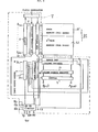
- An IC memory according to the invention comprises an IC memory unit where necessary data is stored nearly permanently and rewrite of data becomes impossible and an IC memory unit where data can be rewritten if necessary, and both IC memory units are constituted on one chip or into one module in hybrid arrangement.
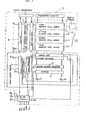
- FIG. 2 is a block constitution diagram of an IC memory as a second embodiment of the invention according to criterion (4) (b) and combination of No. 10 of TAB. 2.
- the IC memory 15 comprises a mask ROM memory cell array 16, PROM memory cell array 17, and EPROM memory cell array 18.
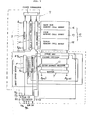
- a storage information read/rewrite apparatus 7 has the same constitution as that of FIG. 1.
- the IC memory When the IC memory is formed in single body of one module, although depending on the capacity of IC memory, it can be made dimension of about diameter 8(mm) x thickness 3(mm) for example.
Landscapes
- Engineering & Computer Science (AREA)
- Computer Hardware Design (AREA)
- Read Only Memory (AREA)
- Stored Programmes (AREA)
- Numerical Control (AREA)
- Techniques For Improving Reliability Of Storages (AREA)
- Static Random-Access Memory (AREA)
Applications Claiming Priority (2)
| Application Number | Priority Date | Filing Date | Title |
|---|---|---|---|
| JP60262870A JPS62121979A (ja) | 1985-11-22 | 1985-11-22 | 集積回路メモリ |
| JP262870/85 | 1985-11-22 |
Publications (2)
| Publication Number | Publication Date |
|---|---|
| EP0224206A2 true EP0224206A2 (de) | 1987-06-03 |
| EP0224206A3 EP0224206A3 (de) | 1990-03-21 |
Family
ID=17381773
Family Applications (1)
| Application Number | Title | Priority Date | Filing Date |
|---|---|---|---|
| EP86116121A Ceased EP0224206A3 (de) | 1985-11-22 | 1986-11-21 | Integrierte Speicherschaltung |
Country Status (3)
| Country | Link |
|---|---|
| US (1) | US4811303A (de) |
| EP (1) | EP0224206A3 (de) |
| JP (1) | JPS62121979A (de) |
Cited By (5)
| Publication number | Priority date | Publication date | Assignee | Title |
|---|---|---|---|---|
| EP0317443A1 (de) * | 1987-11-20 | 1989-05-24 | STMicroelectronics S.A. | Monolithisches elektronisches Bauelement |
| EP0317442A1 (de) * | 1987-11-20 | 1989-05-24 | STMicroelectronics S.A. | Speicher-Ebene und Verfahren und Prototyp zur Bestimmung einer solch eine Speicherebene umfassenden elektronischen integrierten Schaltung |
| US4958324A (en) * | 1987-11-24 | 1990-09-18 | Sgs-Thomson Microelectronics Sa | Method for the testing of electrically programmable memory cells, and corresponding integrated circuit |
| EP0509633A3 (en) * | 1991-03-07 | 1993-02-03 | Sharp Kabushiki Kaisha | Semiconductor memory |
| US7907447B2 (en) | 2006-09-29 | 2011-03-15 | Nxp B.V. | Secure non-volatile memory device and method of protecting data therein |
Families Citing this family (21)
| Publication number | Priority date | Publication date | Assignee | Title |
|---|---|---|---|---|
| DE68928112T2 (de) * | 1988-03-18 | 1997-11-20 | Toshiba Kawasaki Kk | Masken-rom mit Ersatzspeicherzellen |
| JPH0748320B2 (ja) * | 1989-07-24 | 1995-05-24 | セイコー電子工業株式会社 | 半導体不揮発性メモリ |
| JP2547451B2 (ja) * | 1989-09-18 | 1996-10-23 | 富士通株式会社 | 半導体記憶装置 |
| US5485418A (en) * | 1990-01-16 | 1996-01-16 | Mitsubishi Denki Kabushiki Kaisha | Associative memory |
| US5414671A (en) * | 1990-05-01 | 1995-05-09 | Sharp Kabushimi Kaisha | Semiconductor memory device having operation control means with data judging function |
| JPH0475373A (ja) * | 1990-07-18 | 1992-03-10 | Oki Electric Ind Co Ltd | 半導体集積回路装置 |
| JPH04137081A (ja) * | 1990-09-28 | 1992-05-12 | Fuji Photo Film Co Ltd | Eepromを有するicメモリカード |
| JP2724046B2 (ja) * | 1991-02-07 | 1998-03-09 | 富士写真フイルム株式会社 | Icメモリカードシステム |
| US5249160A (en) * | 1991-09-05 | 1993-09-28 | Mosel | SRAM with an address and data multiplexer |
| US5349565A (en) * | 1991-09-05 | 1994-09-20 | Mos Electronics Corporation | SRAM with transparent address latch and unlatched chip enable |
| US5826075A (en) * | 1991-10-16 | 1998-10-20 | International Business Machines Corporation | Automated programmable fireware store for a personal computer system |
| US5878256A (en) * | 1991-10-16 | 1999-03-02 | International Business Machine Corp. | Method and apparatus for providing updated firmware in a data processing system |
| JPH05275657A (ja) * | 1992-03-26 | 1993-10-22 | Toshiba Corp | 半導体記憶装置 |
| JPH06187789A (ja) * | 1992-12-18 | 1994-07-08 | Toshiba Corp | 半導体集積回路装置 |
| JP3550599B2 (ja) * | 1994-02-03 | 2004-08-04 | 株式会社ニコン | イメージセンサーシステム |
| KR0120592B1 (ko) * | 1994-09-09 | 1997-10-20 | 김주용 | 신호 변환 장치를 갖고 있는 어드레스 입력버퍼 |
| KR100318464B1 (ko) * | 1998-06-30 | 2002-02-19 | 박종섭 | 재쓰기회로를갖는스태틱램디바이스 |
| KR100555506B1 (ko) * | 2003-07-11 | 2006-03-03 | 삼성전자주식회사 | 프로그램된 메모리 셀들과 프로그램 및 소거 가능한메모리 셀들을 포함하는 메모리 장치 |
| US7855916B2 (en) | 2007-10-24 | 2010-12-21 | Rao G R Mohan | Nonvolatile memory systems with embedded fast read and write memories |
| US8391086B2 (en) * | 2011-03-04 | 2013-03-05 | Elpida Memory, Inc. | Mask-write apparatus for a SRAM cell |
| US10296480B2 (en) * | 2011-10-20 | 2019-05-21 | SK Hynix Inc. | Data processing system having combined memory block and stack package |
Family Cites Families (13)
| Publication number | Priority date | Publication date | Assignee | Title |
|---|---|---|---|---|
| US3702464A (en) * | 1971-05-04 | 1972-11-07 | Ibm | Information card |
| US4105156A (en) * | 1976-09-06 | 1978-08-08 | Dethloff Juergen | Identification system safeguarded against misuse |
| FR2455320B1 (fr) * | 1979-04-25 | 1986-01-24 | Cii Honeywell Bull | Dispositif de recyclage de supports d'enregistrement identifiables a l'aide de donnees d'identification et composes de memoires monolithiques non volatiles effacables |
| CA1204213A (en) * | 1982-09-09 | 1986-05-06 | Masahiro Takeda | Memory card having static electricity protection |
| US4618943A (en) * | 1984-01-09 | 1986-10-21 | International Business Machines Corporation | Semiconductor static read/write memory having an additional read-only capability |
| US4650981A (en) * | 1984-01-26 | 1987-03-17 | Foletta Wayne S | Credit card with active electronics |
| JPS60144154U (ja) * | 1984-03-07 | 1985-09-25 | シャープ株式会社 | 携帯用電子計算機 |
| US4736094A (en) * | 1984-04-03 | 1988-04-05 | Omron Tateisi Electronics Co. | Financial transaction processing system using an integrated circuit card device |
| JPS6191790A (ja) * | 1984-10-12 | 1986-05-09 | カシオ計算機株式会社 | カ−ド照合装置 |
| US4610000A (en) * | 1984-10-23 | 1986-09-02 | Thomson Components-Mostek Corporation | ROM/RAM/ROM patch memory circuit |
| JPS61160566U (de) * | 1985-03-25 | 1986-10-04 | ||
| US4701601A (en) * | 1985-04-26 | 1987-10-20 | Visa International Service Association | Transaction card with magnetic stripe emulator |
| JPH0818473B2 (ja) * | 1985-07-31 | 1996-02-28 | トッパン・ムーア株式会社 | 機密水準を設定できるicカード |
-
1985
- 1985-11-22 JP JP60262870A patent/JPS62121979A/ja active Pending
-
1986
- 1986-11-21 EP EP86116121A patent/EP0224206A3/de not_active Ceased
- 1986-11-21 US US06/933,156 patent/US4811303A/en not_active Expired - Fee Related
Cited By (10)
| Publication number | Priority date | Publication date | Assignee | Title |
|---|---|---|---|---|
| EP0317443A1 (de) * | 1987-11-20 | 1989-05-24 | STMicroelectronics S.A. | Monolithisches elektronisches Bauelement |
| EP0317442A1 (de) * | 1987-11-20 | 1989-05-24 | STMicroelectronics S.A. | Speicher-Ebene und Verfahren und Prototyp zur Bestimmung einer solch eine Speicherebene umfassenden elektronischen integrierten Schaltung |
| FR2623650A1 (fr) * | 1987-11-20 | 1989-05-26 | Sgs Thomson Microelectronics | Composant electronique monolithique muni d'un decodeur commun pour sa memoire morte et sa memoire de traitement |
| FR2623651A1 (fr) * | 1987-11-20 | 1989-05-26 | Sgs Thomson Microelectronics | Plan memoire et procede et prototype de definition d'un circuit integre electronique comportant un tel plan memoire |
| US5099451A (en) * | 1987-11-20 | 1992-03-24 | Sgs-Thomson Microelectronics S.A. | Memory array with electrically programmable memory cells and electricaly unprogrammable, unerasable memory cells, both types of memory cells having floating gate transistors |
| US4958324A (en) * | 1987-11-24 | 1990-09-18 | Sgs-Thomson Microelectronics Sa | Method for the testing of electrically programmable memory cells, and corresponding integrated circuit |
| EP0509633A3 (en) * | 1991-03-07 | 1993-02-03 | Sharp Kabushiki Kaisha | Semiconductor memory |
| US7907447B2 (en) | 2006-09-29 | 2011-03-15 | Nxp B.V. | Secure non-volatile memory device and method of protecting data therein |
| EP2074629B1 (de) * | 2006-09-29 | 2012-10-24 | Nxp B.V. | Sichere vorrichtung für nicht flüchtige speicher und verfahren zum schutz der darin enthaltenen daten |
| CN101517655B (zh) * | 2006-09-29 | 2012-12-19 | Nxp股份有限公司 | 安全的非易失性存储器件及对其中的数据进行保护的方法 |
Also Published As
| Publication number | Publication date |
|---|---|
| US4811303A (en) | 1989-03-07 |
| JPS62121979A (ja) | 1987-06-03 |
| EP0224206A3 (de) | 1990-03-21 |
Similar Documents
| Publication | Publication Date | Title |
|---|---|---|
| US4811303A (en) | Integrated circuit memory with common address register and decoder | |
| US6256217B1 (en) | Apparatus for on-board programming of serial EEPROMS | |
| EP0154252B1 (de) | Vorrichtung mit programmierbarem Festspeicher und Speicheranordnung zu deren Anwendung | |
| US5668754A (en) | Ferroelectric memory cell and reading/writing method thereof | |
| EP0679996A3 (de) | Halbleiterspeichergerät und Antriebsverfahren | |
| CN1112800A (zh) | 用于微控制器的可遥控改编程序的程序存储器 | |
| Moore | Intel: Memories and the microprocessor | |
| EP0406996A1 (de) | Integrierter Schaltkreis mit einem programmierbaren Schaltkreis | |
| EP0608967A3 (de) | Speicheranordnungen | |
| EP0044978A1 (de) | Lesespeicher | |
| US5280451A (en) | Signature circuit for non-volatile memory device | |
| JPH0466080B2 (de) | ||
| EP0212451A2 (de) | Halbleiterspeicheranordnung mit zwei unabhängigen Spaltenübertragungstortransistorengruppen für Programmierungsschaltung | |
| JP2000030475A (ja) | 半導体メモリ装置 | |
| KR19980064584A (ko) | 불휘발성 반도체 기억 장치와 그 제어 방법, 메모리 카드,및 기억 시스템 | |
| JPS5887644A (ja) | プログラム可能なデジタル情報処理システム | |
| US5153854A (en) | EEPROM memory system having selectable programming voltage for low power readability | |
| GB2090494A (en) | Semiconductor memory device | |
| US20060050580A1 (en) | Method for generating identification code of semiconductor device, method for identifying semiconductor device and semiconductor device | |
| EP1271551B1 (de) | Halbleiterspeicheranordnung und Informationsanordnung | |
| JP3128362B2 (ja) | 半導体装置 | |
| Allan | Components review: Semiconductor memories: More users are opting for RAMs, ROMs, and PROMs as chip function densities increase and price per bit drops | |
| GB2241845A (en) | Voltage adjusting circuit | |
| BR9708365A (pt) | Dispositivo de memória de semicondutor | |
| EP1628309B1 (de) | Verfahren zur Datenorganisation in Speicherzellenmatrix |
Legal Events
| Date | Code | Title | Description |
|---|---|---|---|
| PUAI | Public reference made under article 153(3) epc to a published international application that has entered the european phase |
Free format text: ORIGINAL CODE: 0009012 |
|
| AK | Designated contracting states |
Kind code of ref document: A2 Designated state(s): DE FR GB |
|
| PUAL | Search report despatched |
Free format text: ORIGINAL CODE: 0009013 |
|
| AK | Designated contracting states |
Kind code of ref document: A3 Designated state(s): DE FR GB |
|
| 17P | Request for examination filed |
Effective date: 19900504 |
|
| 17Q | First examination report despatched |
Effective date: 19910604 |
|
| STAA | Information on the status of an ep patent application or granted ep patent |
Free format text: STATUS: THE APPLICATION HAS BEEN REFUSED |
|
| 18R | Application refused |
Effective date: 19930206 |
|
| APAF | Appeal reference modified |
Free format text: ORIGINAL CODE: EPIDOSCREFNE |
|
| RIN1 | Information on inventor provided before grant (corrected) |
Inventor name: HIRAI, HAYAOC/O MITSUBISHI DENKI KABUSHIKI KAISHA |