EP0225962A2 - Transistor à grille isolée à verrouillage inhibé - Google Patents
Transistor à grille isolée à verrouillage inhibé Download PDFInfo
- Publication number
- EP0225962A2 EP0225962A2 EP86107569A EP86107569A EP0225962A2 EP 0225962 A2 EP0225962 A2 EP 0225962A2 EP 86107569 A EP86107569 A EP 86107569A EP 86107569 A EP86107569 A EP 86107569A EP 0225962 A2 EP0225962 A2 EP 0225962A2
- Authority
- EP
- European Patent Office
- Prior art keywords
- well
- gate
- conductivity type
- collector
- igt
- Prior art date
- Legal status (The legal status is an assumption and is not a legal conclusion. Google has not performed a legal analysis and makes no representation as to the accuracy of the status listed.)
- Withdrawn
Links
Images


Classifications
-
- H—ELECTRICITY
- H10—SEMICONDUCTOR DEVICES; ELECTRIC SOLID-STATE DEVICES NOT OTHERWISE PROVIDED FOR
- H10D—INORGANIC ELECTRIC SEMICONDUCTOR DEVICES
- H10D62/00—Semiconductor bodies, or regions thereof, of devices having potential barriers
- H10D62/10—Shapes, relative sizes or dispositions of the regions of the semiconductor bodies; Shapes of the semiconductor bodies
- H10D62/17—Semiconductor regions connected to electrodes not carrying current to be rectified, amplified or switched, e.g. channel regions
- H10D62/393—Body regions of DMOS transistors or IGBTs
Definitions
- This invention relates to power switching transistors, and more specifically to an Insulated Gate Transistor with increased latching current capacity.
- bipolar transistors bipolar ("majority” and “minority” carrier) conduction through PN junctions and a large base area permits a high current density.
- PN junctions have a capacitance that must be charged in turning the transistor on, and discharged in turning it off, which slows the switching speed of bipolar transistors.
- excess minority and majority carriers in the base when the transistor begins to turn off must recombine before the transistor is completely turned off.
- the voltage and current through the transistor change, in opposite directions, and at intermediate values their product, power, is higher than when the transistor is not switching.
- the transistor dissipates power as heat.
- the ability of silicon to dissipate heat limits the current density rating of bipolar transistors placed in a given area of semiconductor material.
- a metal oxide semiconductor field effect transistor switches faster and dissipates less heat than a bipolar transistor of the same rating.
- a MOSFET is operated by applying a voltage potential to its gate electrode to establish an electric field from the gate through a layer of gate oxide and into underlying semiconductor material. The field inverts charges in an adjacent channel region beneath the oxide in the semiconductor material, which enables a current of majority charge carriers to flow between appropriately biased source and drain regions connected by the channel region. Having no counter-current of minority charge carriers in need of recombining with majority charge carriers, MOSFETs switch on and off very rapidly. Yet, with the channel being the only conduction path, a MOSFET does not conduct as much current as a same-size bipolar transistor rated for the same voltage. Consequently, MOSFETs have a lower current density.
- An ideal power switching device would switch on and off at high speed in MOSFET mode, to conduct current at high density in bipolar mode when on, and be controllable by a gate electrode.
- Vertical MOS and double diffused MOS (DMOS) transistors are MOSFET structures adapted for power switching, i.e. switching large currents on and off.
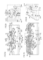
- a typical prior art DMOS transistor 10 an N-type semiconductor substrate with upper surface 12 provides a drain region 18.
- Drain 18 includes upper drain region 18ub and lower drain region 181.
- Backside terminal 15 contacts drain 18.
- Gate oxide layer 20 on surface 12 supports and insulates polysilicon gate 22b above upper drain 18ub.
- a P-type semiconductor channel body well such as well 24a has a thin wall 25b for forming conduction channel 26b beneath upper surface 12.
- P type well 24a contains source region 28b, which is heavily doped with N-type impurities.
- each source region 28a,b,c,d is adjacent one of gates 22a, 22b and 22c.
- Each gate 22a, 22b, 22c bridges a respective upper drain region 18ua, 18ub, 18uc separating two adjacent well regions 24.
- Structure 10 is bilaterally symmetrical about an imaginary vertical center plane along center line C L (Fig. 1a) through the center of gate 22b and perpendicular to the plane of the drawing.
- Fig. 1b With a gate voltage applied to gate 22b which is greater than the conduction threshold voltage for channel 26b, and with drain 18 biased positively an appropriate amount with respect to source 28b, electrons flow from source 28b through channel 26b to upper drain 18ub, as indicated by the e ⁇ arrow, and flow out drain terminal 15 (Fig. 1a). If source-well junction 27b becomes forward biased by more than 0.7 volts, thin and lightly doped well wall 25b functions as a base of a parasitic bipolar transistor. Electrons flow from source 28b not only through channel 26b but across forward biased junction 27b and through other parts of well 24a, and across junction 34a into lower drain 181.
- the source-channel-drain structure works as a parasitic emitter-base-collector bipolar transistor. Bipolar conduction continues uncontrolled, even after gate lead 30b is externally shorted to emitter lead 32a to eliminate the field forming channel 26b and stop FET conduction. To stop bipolar conduction, the source-to-drain voltage difference must be externally reduced until junction 27b is no longer forward biased by as much as 0.7 volts.
- source region 28b and well 24a are typically shorted together by a source-emitter aluminum contact terminal 32a positioned on wafer surface 12 at point "S" (Fig. 1b) where source-well junction 27b meets surface 12, remote from channel 26b since shorting junction 27b adjacent channel 26b would interface with current through the channel. Still, at a sufficient source-drain bias voltage (30 to 1000 volts, depending on the design, and hence rating, of device 10), reverse biased well-drain junction 34a breaks down, and a hole current starts from drain 18 across junction 34a and through well 24a.
- forward biasing of junction 27b can be deterred if the voltage drop along path 50 is reduced, by narrowing source region 28b to shorten path 50, or by decreasing the resistivity of semiconductor material in the path.
- U.S. Patent 4,345,265 to Blanchard reduces the current and voltage difference along a path 50 in a DMOS transistor by selectively enlarging and increasing the conductivity of well 24 remote from channel 26 to form a "deep well" 66 (not shown for a DMOS transistor but shown in Fig. 2a for an IGT) to divert hole current from path 50.
- the P type conductivity of well 24a cannot be increased in well wall 25b near upper drain 18ub because that would prevent the field applied by gate 22b from inverting the conductivity of that region to form a conducting channel 26b.
- the deep well 66a portion of well 24a provides a more constant breakdown voltage along junction 34a.
- the conductivity of well 24a being increased in the portion of deep well 66a near contact 32a provides a lower resistance path or short between the interior of well 24a and source region 28b.
- the increased current density of DMOS transistors with deep wells 66 is still not comparable to that of bipolar transistors, and, for similar voltage ratings and die areas, DMOS transistors generally have a higher "on" resistance than bipolar transistors.
- An insulated gate transistor is a dual mode DMOS-like structure which switches on at high speed in MOS mode and obtains controlled high density conduction in bipolar mode.
- Fig. 2a (not to scale) shows a prior art IGT device. The regions in each space in Fig. 2a between the vertical axes of a gate terminal 30 on one side and a source-collector terminal 32 on the other side form respective IGTs 60a, 60b, 60c, and 60d.
- Fig. 2b shows the equivalent circuit for an IGT superimposed over the regions forming an IGT 60, with junctions 27, 34, and 67 indicated by dashed lines.
- an IGT such as 60b comprises four layers, in which three layers or regions 28b, 24a, and 18 of N+, P-, and N- type semiconductor material, respectively, are used for a source, channel body, and drain in an N-channel FET structure as in a DMOS transistor.
- corresponding regions of the structures of Figs. 1a and 2a are numbered the same.
- Three lower regions 24a, 18, and 62 of P+, N-, and P+ type material, respectively, are used for a collector, base, and emitter in a bipolar transistor structure QL.
- the added fourth layer P+ emitter region (Fig. 2a) is provided by substrate 62, on which regions 18 are epitaxially grown.
- IGT 60b When starting to turn on, IGT 60b operates only in FET mode. While turning on, forward biased junction 67 makes region 62 function as part of drain 181. When IGT 60b completes turning on, however, regions of IGT 60b also function in bipolar mode. Thus region 18 functions not only as a drain of an FET but also as the base of bipolar transistor QL, and well 24a functions not only as channel of an FET but also as the collector 24 of transistor QL (Fig. 2b).
- P-implanted wells 24a and 24b (Fig. 2a) contain, in regions closely adjacent to but separated from upper drain region 18ub, N-implanted source regions 28b and 28c, respectively.
- the laterally opposed sides of each well 24a and 24b contain, as shown in Fig.
- Source regions 28a, 28b, 28c and 28d are respectively formed between source regions 28a, 28b, 28c and 28d on the one hand, and the directly adjacent upper drain regions 18ua, 18ub, and 18uc, on the other hand.
- a positive potential at terminal 68 relative the potential at terminal 32a reverse biases junction 34a and blocks forward current.
- the base of transistor QL Fig. 2b
- IGT 60b in Fig. 2a when a positive voltage is applied to gate 22b, and drain region 18 is biased positive relative to source region 28b, electrons flow through channel 26b.
- This FET mode electron conduction provides a base current for bipolar transistor QL.
- FET mode electron current through forward biased junction 67 towards emitter 62 causes an opposite current of holes to be injected from emitter 62 back across junction 67.
- Minority carrier holes in base region 18 combine with electrons or are swept across reverse biased junction 34a to collector 24a of transistor QL.
- Bipolar conduction in an IGT increases (improves) current density over a DMOSFET, by as much as a factor of 19 (IEEE Trans. on Electron Devices, Vol. ED-31, No. 6, June 84, pg. 821).
- Bipolar mode conduction is intended in the three regions 62, 18, and 24a, respectively, which form PNP transistor QL in the lower three regions of IGT 60b.
- regions 62, 18 and 24a, plus fourth region 28b unfortunately constitute a thyristor.
- the collector current of transistor QL along path 50 sufficiently forward biases portions of junction 27b removed from terminal 32a, the three regions 18, 24a, and 28b operate as a parasitic bipolar NPN transistor QP (Fig. 2b).
- the four layer thyristor structure 60b With transistors QL and QP both conducting, the four layer thyristor structure 60b "latches" into a self-perpetuating state of bipolar conduction, which cannot be turned off by removing the voltage bias on gate 22b to stop FET mode conduction. Thus control through gate 22b over the bipolar current is lost.
- Regions of IGTs 60a, 60c, and 60d function identically to correspondingly numbered but differently lettered regions of IGT 60b.
- An enlarged and more conductive well 66a diverts some current from critical path 50 and increases the latching current density of IGT 60b.
- collector wells of increased size and conductivity are of limited effectiveness in diverting current from critical path 50. Hole current tends to flow only within a diffusion length of the electron current path (which is through channel 26b), so not enough hole current is diverted through deep well 66a. Controllable current density ratings of conventional IGTs are still limited by latching caused by current along critical path 50. It is therefore desirable to further increase the latching current density of IGTs to expand their range of reliable and useful operation.
- This invention increases the latching current density of an IGT by providing a highly conductive collector well region laterally adjacent the gate, to create an alternate current path for bipolar current and offset current flowing in a critical path parallel to the source region junction in the pinched region of the collector well.
- the separate, high conductivity collector well region collects most or all of the hole current which, in prior art IGT devices, would flow along the critical path.
- the current at which the junction between the collector well and the source region becomes forward biased is substantially increased over the prior art and the resulting IGT of this invention operates at a higher and more useful current density without latching.
- an IGT of given dimensions processed using the same design rules as the prior art can, at a given voltage, handle a current 100% greater than the prior art device, or can, at a given current, handle a biasing voltage (between terminals 68 and 32a of Fig. 2a) 50% lower than the prior art device.
- the present invention modifies insulated gate transistors to reduce their susceptibility to latching, thereby increasing their current density rating.
- the invention is illustrated in a preferred embodiment as IGT 70 in Figs. 3a, 3b, and 3c, which are not drawn to scale.
- IGT 70 has a collector well 76b, laterally adjacent drain region 18ub below one side of gate 22b, which is larger and more conductive than collector well 24a.
- IGT 70 includes regions which correspond to and are numbered the same as regions of conventional DMOS FET 10 or IGT 60b shown in Figs. 1a, 1b, and 2a.
- IGT 70 of this invention differs from prior art IGT devices in that instead of having adjacent IGT's 60b and 60c share gate 22b which bridges a pair of prior art collector wells 24a and 24b, each containing a respective source region 28b and 28c, IGT 70 has one collector well 24a which contains a source region 28b, and has a second collector well 76b which, unlike IGTs 60, does not contain a source region 28c, and does not have a pinched low conductivity region 23 for forming a channel 26.
- Transistor QL in the circuit of Fig. 2b is modified by the invention as shown in Fig. 3b to form transistor QL ⁇ including second collector region 76b, which is not contiguous with a source region 28.
- IGT 70 as shown in Fig. 3a can be expanded to form a larger IGT device as shown in the partially cut away isometric view of Fig. 3c.
- a center provided by collector well 24a, and surrounding concentric squares 28, 22, 18u and 76 together form an IGT cell 70, with outer corners Clf, Crf, Clr, and Crr at the centers of adjacent octagonal-shaped regions 76
- sources 28a and 28b are two parts of the same region 28, and gates 22a and 22b are two parts of a continuous gate layer 22.
- the cell pattern is repeated by adjacent cells, each centered on a respective collector 24 and sharing one side with cell 70.
- the eight collector regions 76 forming the corners and sides of a given cell are connected by lateral diffusions under wafer surface 12 beneath portions of gate layer 22.
- Gate layer 22 crosses these diffused connections between regions 76 in order that polycrystalline silicon 22 for all cells can be connected together to one terminal preferably at a lateral edge of overlying collector metallization 32.
- polycrystalline silicon 22 can be masked and etched (in the steps of Figs. 4 and 7) so that wells 76 extend (not shown) under gate 22 towards collector regions 24, or end at the edge of gates 22 as shown in Fig. 3c, or are spaced from the edges of gates 22 as shown in Figs. 8, 9, 9a, and 3a.
- IGT 70 is switched on by applying appropriate bias voltages to source terminal 32a, (which is preferably connected by metallization 32 to collector 76 surface 33), gate terminal 30 (not shown in Fig. 3a or 3c, but connected to polysilicon layer 32 in a convenient place), and drain/emitter terminal 63 to cause FET mode conduction of electrons from source 28b to upper drain 18ub.
- FET mode current density is less than bipolar mode current density, FET switching is faster.
- FET mode current to upper drain 18ub from only one source 28b on one (the left) side of region 18ub is less than the current from sources 28 on both sides as in conventional shared gate IGT devices 60.
- FET mode electron conduction through drain region 18 also serves as a base current which turns on bipolar transistor QL ⁇ (Fig. 3b) causing a bipolar current of holes from emitter 62 through base 18 and, primarily, out collector 76b.
- the FET mode current from a source 28b on one side to upper drain 18u provides sufficient current to saturate transistor QL ⁇ .
- the current through IGT 70 can be controlled, i.e. stopped, over a wider nonlatching range than a prior art IGT 60, as explained above, by eliminating the channel field under gate 22b, for example, by shorting the gate terminal (not shown) to source terminal 32a to stop FET mode conduction and cut off current to base region 18 of transistor QL ⁇ .
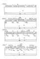
- an IGT 70 with highly conductive collector wells 76 can be made as follows. Referring to Figure 4, the process starts with a P+ conductivity type semiconductor substrate 62 on which a layer 11, lightly doped with N type dopants to a concentration of approximately 1014 atoms/cm3, is epitaxially grown to a thickness of approximately 80 to 100 microns. In the actual integrated circuit structure, the thickness of the epitaxial layer comprising drain/base 18 is about 100 microns or about 20 times the approximately 5 micron depth of to-be-formed wells 66 and 76.
- Top surface 12 of epitaxial layer 11 is covered with a layer of gate oxide 20, about 0.1 microns thick, and then covered with a layer of polycrystalline silicon 22 about 0.7 microns thick.
- a layer of photoresist is deposited on polysilicon 22 and patterned to form a first mask, not shown.
- the interval or "pitch" between repetitions of IGT cells 70 in the completed integrated circuit for example between the axes of wells 76a and 76b in Fig. 5, or between left front corner Clf and right front corner Clr in Fig. 3c, is preferably about 50 microns.
- polysilicon 22 and gate oxide 20 are removed to form openings through which impurities will be passed to form P+ wells 76 (Fig. 5) and N+ sources 28 (Fig. 6) in the epitaxial layer.
- the openings over source areas 28 are covered by a second mask M2 of photoresist, and well regions 76 are P+ doped to a concentration of about 1016 to 1017 atoms/cm3 by ion implantation to a depth of about 5 microns.
- the second mask is removed, and a third mask M3 of photoresist is formed over well openings 76, as shown in Figure 6.
- the exposed source areas 28, about six microns wide, are then N+ doped by ion implantation with N type dopants to a concentration of 5x10¹⁹ atoms/cm3 to a depth of about 1 micron.
- the third mask M3 is removed, and, as shown in Figure 7, a fourth mask M4 is formed over the approximately 6 micron wide parts of polysilicon 22 that will be retained as gates 22.
- the fourth mask may overlap the edges of the gates adjacent sources 28. Exposed areas of polysilicon 22, i.e., surrounding wells 76 between gates 22, and between source areas 28, are then removed.
- collector well 76 metallization 32 can be insulated by SiO2 layer 29, Fig. 3c, close enough to polysilicon layer 22 and if biasing levels permit, wells 76 can extend (not shown) under gates 22.
- a fifth mask M5 of photoresist is formed covering the just-enlarged areas around wells 76.
- the exposed surface 12 between pairs of source areas 28, and source areas 28 themselves, are then lightly doped with P type deposits to a concentration of about 1014 atoms/cm3 to form wells 24, which diffuse laterally through sources 28 to form a pinched region in which thin walls 25 provide channels 26 approximately 3 microns wide under gates 22.
- a sixth mask M6 is formed, as shown in Figure 9, covering the surface of the structure except between wells 28, which is heavily doped with P ions to a concentration of 1017 to 1018 atoms/cm3. Deep walls 66 are typically not as deep or as conductive as primary collector well 76.
- Sixth mask M6 is removed and a layer of oxide 29 (Fig. 3a) is formed over the entire structure.
- a seventh mask (not shown) is used in removing the oxide except around gates 22. The oxide mask is removed.
- An eighth mask (not shown) is used to form conductor metallizations, typically of aluminum, for gate and well contacts 30 and 32. This produces the structure shown in Fig. 3a.
- step 9 and the sixth mask M6 are omitted.
- a layer of gate-insulating oxide is formed everywhere on the structure, and a seventh mask, not shown, is used to remove oxide 29 except around gates 22, as shown in Figures 9a and 3c.
- the wafer is then covered with a source contact metal layer 32 and gate terminals 30 (not shown) contacting gate polysilicon 22 typically at the lateral edge of the IGT device.
- a ninth mask (not shown) is applied to form bonding pad windows for leads around the periphery of the circuit, and leads are attached.
- the entire device is typically covered with a passivating (protective) layer (not shown) over metal layer 32.
Landscapes
- Insulated Gate Type Field-Effect Transistor (AREA)
- Metal-Oxide And Bipolar Metal-Oxide Semiconductor Integrated Circuits (AREA)
- Electronic Switches (AREA)
Applications Claiming Priority (2)
| Application Number | Priority Date | Filing Date | Title |
|---|---|---|---|
| US06/808,904 US4779123A (en) | 1985-12-13 | 1985-12-13 | Insulated gate transistor array |
| US808904 | 1985-12-13 |
Publications (2)
| Publication Number | Publication Date |
|---|---|
| EP0225962A2 true EP0225962A2 (fr) | 1987-06-24 |
| EP0225962A3 EP0225962A3 (fr) | 1988-01-07 |
Family
ID=25200068
Family Applications (1)
| Application Number | Title | Priority Date | Filing Date |
|---|---|---|---|
| EP86107569A Withdrawn EP0225962A3 (fr) | 1985-12-13 | 1986-06-04 | Transistor à grille isolée à verrouillage inhibé |
Country Status (3)
| Country | Link |
|---|---|
| US (1) | US4779123A (fr) |
| EP (1) | EP0225962A3 (fr) |
| JP (1) | JP2574267B2 (fr) |
Cited By (6)
| Publication number | Priority date | Publication date | Assignee | Title |
|---|---|---|---|---|
| FR2641417A1 (fr) * | 1988-12-29 | 1990-07-06 | Fuji Electric Co Ltd | Dispositif a semi-conducteur de type mos |
| EP0416805A3 (en) * | 1989-08-30 | 1991-03-27 | Siliconix, Inc. | Transistor with voltage clamp |
| CH679962A5 (fr) * | 1989-08-10 | 1992-05-15 | Asea Brown Boveri | |
| EP0563952A1 (fr) * | 1992-04-03 | 1993-10-06 | Hitachi, Ltd. | Dispositif semi-conducteur à injection de trous améliorée |
| EP0683530A3 (fr) * | 1988-11-07 | 1996-01-03 | Mitsubishi Electric Corp | |
| WO1998006136A1 (fr) * | 1996-08-01 | 1998-02-12 | Siemens Aktiengesellschaft | Element a semiconducteur pouvant etre commande par effet de champ |
Families Citing this family (19)
| Publication number | Priority date | Publication date | Assignee | Title |
|---|---|---|---|---|
| JPH0758783B2 (ja) * | 1986-04-09 | 1995-06-21 | 富士電機株式会社 | 導電変調型mosfet |
| US4926074A (en) * | 1987-10-30 | 1990-05-15 | North American Philips Corporation | Semiconductor switch with parallel lateral double diffused MOS transistor and lateral insulated gate transistor |
| JPH0648729B2 (ja) * | 1988-02-24 | 1994-06-22 | シーメンス、アクチエンゲゼルシシヤフト | 電界効果制御可能のバイポーラ・トランジスタ |
| US4931844A (en) * | 1988-03-09 | 1990-06-05 | Ixys Corporation | High power transistor with voltage, current, power, resistance, and temperature sensing capability |
| US5159425A (en) * | 1988-06-08 | 1992-10-27 | Ixys Corporation | Insulated gate device with current mirror having bi-directional capability |
| US4942445A (en) * | 1988-07-05 | 1990-07-17 | General Electric Company | Lateral depletion mode tyristor |
| EP0371785B1 (fr) * | 1988-11-29 | 1996-05-01 | Kabushiki Kaisha Toshiba | MOSFET latéral à modulation de conductivité |
| US4998160A (en) * | 1989-01-23 | 1991-03-05 | Motorola, Inc. | Substrate power supply contact for power integrated circuits |
| TW399774U (en) * | 1989-07-03 | 2000-07-21 | Gen Electric | FET, IGBT and MCT structures to enhance operating characteristics |
| EP0409010A1 (fr) * | 1989-07-19 | 1991-01-23 | Asea Brown Boveri Ag | Dispositif semi-conducteur de puissance, à extinction |
| US5063307A (en) * | 1990-09-20 | 1991-11-05 | Ixys Corporation | Insulated gate transistor devices with temperature and current sensor |
| JPH05206469A (ja) * | 1992-01-29 | 1993-08-13 | Hitachi Ltd | 絶縁ゲート型バイポーラトランジスタ |
| JP2818348B2 (ja) * | 1993-03-01 | 1998-10-30 | 株式会社東芝 | 半導体装置 |
| US6770911B2 (en) * | 2001-09-12 | 2004-08-03 | Cree, Inc. | Large area silicon carbide devices |
| US7279743B2 (en) | 2003-12-02 | 2007-10-09 | Vishay-Siliconix | Closed cell trench metal-oxide-semiconductor field effect transistor |
| US8183629B2 (en) * | 2004-05-13 | 2012-05-22 | Vishay-Siliconix | Stacked trench metal-oxide-semiconductor field effect transistor device |
| US8471390B2 (en) | 2006-05-12 | 2013-06-25 | Vishay-Siliconix | Power MOSFET contact metallization |
| US8368126B2 (en) | 2007-04-19 | 2013-02-05 | Vishay-Siliconix | Trench metal oxide semiconductor with recessed trench material and remote contacts |
| US9306056B2 (en) | 2009-10-30 | 2016-04-05 | Vishay-Siliconix | Semiconductor device with trench-like feed-throughs |
Family Cites Families (14)
| Publication number | Priority date | Publication date | Assignee | Title |
|---|---|---|---|---|
| US3391452A (en) * | 1966-05-16 | 1968-07-09 | Hewlett Packard Co | Method of making a reliable low-ohmic nonrectifying connection to a semiconductor substrate |
| US4364073A (en) * | 1980-03-25 | 1982-12-14 | Rca Corporation | Power MOSFET with an anode region |
| US4344081A (en) * | 1980-04-14 | 1982-08-10 | Supertex, Inc. | Combined DMOS and a vertical bipolar transistor device and fabrication method therefor |
| DE3103444A1 (de) * | 1981-02-02 | 1982-10-21 | Siemens AG, 1000 Berlin und 8000 München | Vertikal-mis-feldeffekttransistor mit kleinem durchlasswiderstand |
| FR2507820A1 (fr) * | 1981-06-16 | 1982-12-17 | Thomson Csf | Transistor bipolaire a commande par effet de champ au moyen d'une grille isolee |
| DE3224618A1 (de) * | 1982-07-01 | 1984-01-05 | Siemens AG, 1000 Berlin und 8000 München | Igfet mit ladungstraegerinjektion |
| US4743952A (en) * | 1983-04-04 | 1988-05-10 | General Electric Company | Insulated-gate semiconductor device with low on-resistance |
| GB2150753B (en) * | 1983-11-30 | 1987-04-01 | Toshiba Kk | Semiconductor device |
| JPS60249367A (ja) * | 1984-05-25 | 1985-12-10 | Hitachi Ltd | 絶縁ゲ−ト形トランジスタ |
| JPS60254658A (ja) * | 1984-05-30 | 1985-12-16 | Toshiba Corp | 導電変調型mosfet |
| US4672407A (en) * | 1984-05-30 | 1987-06-09 | Kabushiki Kaisha Toshiba | Conductivity modulated MOSFET |
| US4631564A (en) * | 1984-10-23 | 1986-12-23 | Rca Corporation | Gate shield structure for power MOS device |
| JPH0620141B2 (ja) * | 1985-03-28 | 1994-03-16 | 株式会社東芝 | 導電変調型mosfet |
| US4682195A (en) * | 1985-09-30 | 1987-07-21 | General Electric Company | Insulated gate device with configured emitter contact pad |
-
1985
- 1985-12-13 US US06/808,904 patent/US4779123A/en not_active Expired - Lifetime
-
1986
- 1986-06-04 EP EP86107569A patent/EP0225962A3/fr not_active Withdrawn
- 1986-12-12 JP JP61295052A patent/JP2574267B2/ja not_active Expired - Lifetime
Cited By (8)
| Publication number | Priority date | Publication date | Assignee | Title |
|---|---|---|---|---|
| EP0683530A3 (fr) * | 1988-11-07 | 1996-01-03 | Mitsubishi Electric Corp | |
| FR2641417A1 (fr) * | 1988-12-29 | 1990-07-06 | Fuji Electric Co Ltd | Dispositif a semi-conducteur de type mos |
| CH679962A5 (fr) * | 1989-08-10 | 1992-05-15 | Asea Brown Boveri | |
| EP0416805A3 (en) * | 1989-08-30 | 1991-03-27 | Siliconix, Inc. | Transistor with voltage clamp |
| US5945723A (en) * | 1992-04-02 | 1999-08-31 | Hitachi, Ltd. | Composite controlled semiconductor device |
| EP0563952A1 (fr) * | 1992-04-03 | 1993-10-06 | Hitachi, Ltd. | Dispositif semi-conducteur à injection de trous améliorée |
| US5780917A (en) * | 1992-04-03 | 1998-07-14 | Hitachi, Ltd. | Composite controlled semiconductor device and power conversion device using the same |
| WO1998006136A1 (fr) * | 1996-08-01 | 1998-02-12 | Siemens Aktiengesellschaft | Element a semiconducteur pouvant etre commande par effet de champ |
Also Published As
| Publication number | Publication date |
|---|---|
| JPS62145777A (ja) | 1987-06-29 |
| EP0225962A3 (fr) | 1988-01-07 |
| US4779123A (en) | 1988-10-18 |
| JP2574267B2 (ja) | 1997-01-22 |
Similar Documents
| Publication | Publication Date | Title |
|---|---|---|
| US4779123A (en) | Insulated gate transistor array | |
| JP2585331B2 (ja) | 高耐圧プレーナ素子 | |
| JP5357370B2 (ja) | 半導体デバイス | |
| US5321281A (en) | Insulated gate semiconductor device and method of fabricating same | |
| KR100194661B1 (ko) | 전력용 트랜지스터 | |
| EP0581246A2 (fr) | Dispositif à semiconducteur du type MOS | |
| JPH05198800A (ja) | 絶縁ゲートバイポーラトランジスタ | |
| JPS60253275A (ja) | 高密度v溝型mos制御型サイリスタ、絶縁ゲ−ト型トランジスタおよびmosfet、並びに製造方法 | |
| JPH02275675A (ja) | Mos型半導体装置 | |
| JP3400025B2 (ja) | 高耐圧半導体素子 | |
| CN115332354A (zh) | 优化短路电流耐受能力的碳化硅mosfet结构 | |
| US5381025A (en) | Insulated gate thyristor with gate turn on and turn off | |
| EP0630054B1 (fr) | Thyristor à grille isolée et procédé de mise en service | |
| US5757034A (en) | Emitter switched thyristor | |
| JPH04261065A (ja) | 半導体装置 | |
| JPH10321859A (ja) | 寄生サイリスターラッチアップを防止するために不連続のエミッター領域を含む電力半導体装置 | |
| JP2814079B2 (ja) | 半導体集積回路とその製造方法 | |
| EP0253353B1 (fr) | Dispositif semi-conducteur composite | |
| EP0540017B1 (fr) | Thyristor à commande de grille de type MOS | |
| WO1991003078A1 (fr) | Thyristor a grille isolee interruptible | |
| JP3505220B2 (ja) | 絶縁ゲート型半導体装置 | |
| EP0144654A2 (fr) | Dispositif semi-conducteur comportant un transistor à effet de champ à porte isolée, diélectriquement isolé | |
| JPH07142731A (ja) | パワーデバイスおよびそれを形成するための方法 | |
| US5489788A (en) | Insulated gate semiconductor device with improved short-circuit tolerance | |
| JP3393932B2 (ja) | 絶縁ゲート型半導体装置 |
Legal Events
| Date | Code | Title | Description |
|---|---|---|---|
| PUAI | Public reference made under article 153(3) epc to a published international application that has entered the european phase |
Free format text: ORIGINAL CODE: 0009012 |
|
| AK | Designated contracting states |
Kind code of ref document: A2 Designated state(s): BE DE FR GB IT NL |
|
| PUAL | Search report despatched |
Free format text: ORIGINAL CODE: 0009013 |
|
| AK | Designated contracting states |
Kind code of ref document: A3 Designated state(s): BE DE FR GB IT NL |
|
| 17P | Request for examination filed |
Effective date: 19880420 |
|
| STAA | Information on the status of an ep patent application or granted ep patent |
Free format text: STATUS: THE APPLICATION HAS BEEN WITHDRAWN |
|
| 18W | Application withdrawn |
Withdrawal date: 19880614 |
|
| RIN1 | Information on inventor provided before grant (corrected) |
Inventor name: COGAN, ADRIAN I. Inventor name: BENCUYA, IZAK |